EP2284580A1 - Optischer film und herstellungsverfahren dafür, blendfreier film, polarisierungselement mit optischer schicht und anzeigevorrichtung - Google Patents
Optischer film und herstellungsverfahren dafür, blendfreier film, polarisierungselement mit optischer schicht und anzeigevorrichtung Download PDFInfo
- Publication number
- EP2284580A1 EP2284580A1 EP09762498A EP09762498A EP2284580A1 EP 2284580 A1 EP2284580 A1 EP 2284580A1 EP 09762498 A EP09762498 A EP 09762498A EP 09762498 A EP09762498 A EP 09762498A EP 2284580 A1 EP2284580 A1 EP 2284580A1
- Authority
- EP
- European Patent Office
- Prior art keywords
- fine particles
- weight
- optical
- coating material
- less
- Prior art date
- Legal status (The legal status is an assumption and is not a legal conclusion. Google has not performed a legal analysis and makes no representation as to the accuracy of the status listed.)
- Withdrawn
Links
Images









Classifications
-
- G—PHYSICS
- G02—OPTICS
- G02B—OPTICAL ELEMENTS, SYSTEMS OR APPARATUS
- G02B5/00—Optical elements other than lenses
- G02B5/02—Diffusing elements; Afocal elements
- G02B5/0273—Diffusing elements; Afocal elements characterized by the use
- G02B5/0278—Diffusing elements; Afocal elements characterized by the use used in transmission
-
- G—PHYSICS
- G02—OPTICS
- G02B—OPTICAL ELEMENTS, SYSTEMS OR APPARATUS
- G02B5/00—Optical elements other than lenses
- G02B5/02—Diffusing elements; Afocal elements
- G02B5/0205—Diffusing elements; Afocal elements characterised by the diffusing properties
- G02B5/021—Diffusing elements; Afocal elements characterised by the diffusing properties the diffusion taking place at the element's surface, e.g. by means of surface roughening or microprismatic structures
- G02B5/0226—Diffusing elements; Afocal elements characterised by the diffusing properties the diffusion taking place at the element's surface, e.g. by means of surface roughening or microprismatic structures having particles on the surface
-
- G—PHYSICS
- G02—OPTICS
- G02B—OPTICAL ELEMENTS, SYSTEMS OR APPARATUS
- G02B5/00—Optical elements other than lenses
- G02B5/02—Diffusing elements; Afocal elements
- G02B5/0273—Diffusing elements; Afocal elements characterized by the use
- G02B5/0284—Diffusing elements; Afocal elements characterized by the use used in reflection
-
- G—PHYSICS
- G02—OPTICS
- G02B—OPTICAL ELEMENTS, SYSTEMS OR APPARATUS
- G02B1/00—Optical elements characterised by the material of which they are made; Optical coatings for optical elements
- G02B1/10—Optical coatings produced by application to, or surface treatment of, optical elements
- G02B1/11—Anti-reflection coatings
-
- G—PHYSICS
- G02—OPTICS
- G02F—OPTICAL DEVICES OR ARRANGEMENTS FOR THE CONTROL OF LIGHT BY MODIFICATION OF THE OPTICAL PROPERTIES OF THE MEDIA OF THE ELEMENTS INVOLVED THEREIN; NON-LINEAR OPTICS; FREQUENCY-CHANGING OF LIGHT; OPTICAL LOGIC ELEMENTS; OPTICAL ANALOGUE/DIGITAL CONVERTERS
- G02F1/00—Devices or arrangements for the control of the intensity, colour, phase, polarisation or direction of light arriving from an independent light source, e.g. switching, gating or modulating; Non-linear optics
- G02F1/01—Devices or arrangements for the control of the intensity, colour, phase, polarisation or direction of light arriving from an independent light source, e.g. switching, gating or modulating; Non-linear optics for the control of the intensity, phase, polarisation or colour
- G02F1/13—Devices or arrangements for the control of the intensity, colour, phase, polarisation or direction of light arriving from an independent light source, e.g. switching, gating or modulating; Non-linear optics for the control of the intensity, phase, polarisation or colour based on liquid crystals, e.g. single liquid crystal display cells
- G02F1/133—Constructional arrangements; Operation of liquid crystal cells; Circuit arrangements
- G02F1/1333—Constructional arrangements; Manufacturing methods
- G02F1/1335—Structural association of cells with optical devices, e.g. polarisers or reflectors
- G02F1/133502—Antiglare, refractive index matching layers
-
- G—PHYSICS
- G02—OPTICS
- G02F—OPTICAL DEVICES OR ARRANGEMENTS FOR THE CONTROL OF LIGHT BY MODIFICATION OF THE OPTICAL PROPERTIES OF THE MEDIA OF THE ELEMENTS INVOLVED THEREIN; NON-LINEAR OPTICS; FREQUENCY-CHANGING OF LIGHT; OPTICAL LOGIC ELEMENTS; OPTICAL ANALOGUE/DIGITAL CONVERTERS
- G02F2202/00—Materials and properties
- G02F2202/36—Micro- or nanomaterials
-
- Y—GENERAL TAGGING OF NEW TECHNOLOGICAL DEVELOPMENTS; GENERAL TAGGING OF CROSS-SECTIONAL TECHNOLOGIES SPANNING OVER SEVERAL SECTIONS OF THE IPC; TECHNICAL SUBJECTS COVERED BY FORMER USPC CROSS-REFERENCE ART COLLECTIONS [XRACs] AND DIGESTS
- Y10—TECHNICAL SUBJECTS COVERED BY FORMER USPC
- Y10T—TECHNICAL SUBJECTS COVERED BY FORMER US CLASSIFICATION
- Y10T428/00—Stock material or miscellaneous articles
- Y10T428/24—Structurally defined web or sheet [e.g., overall dimension, etc.]
- Y10T428/24355—Continuous and nonuniform or irregular surface on layer or component [e.g., roofing, etc.]
- Y10T428/24372—Particulate matter
Definitions
- the present invention relates to an optical film and a method for manufacturing the same, an antiglare film, a polarizer with an optical layer, and a display apparatus.
- it relates to an optical film used in a display surface of a display apparatus such as a liquid crystal display apparatus.
- the former method has the following problems.
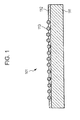
- an antiglare film 101 includes a base material 111 and an antiglare layer 112 provided on the base material 111.
- the antiglare layer 112 is constituted by a resin containing fine particles 113 composed of amorphous silica or resin beads. Fine irregularities are formed on the surface by protruding the fine particles 113 from the surface of the antiglare layer 112.
- This antiglare film 101 is formed by applying a coating material containing the fine particles 113, a resin, a solvent, and the like onto the base material 111 and curing the coating material. According to the antiglare film 101 having the above structure, since the fine irregularities on the surface of the antiglare layer 112 scatter light incident on the antiglare layer 112, reflection due to surface reflection is reduced.
- the fine irregularities on the surface of the antiglare film 101 are constituted by the fine particles 113 protruding on the surface and a binder portion that connects between protrusions of the fine particles 113 with continuous slopes. Accordingly, although the antiglare film 101 has a high antiglare property, light that is transmitted through the antiglare layer 112 in the vertical direction is also strongly scattered, resulting in a problem of a decrease in the transmitted image clarity.
- a conceivable approach to suppress the decrease in the transmitted image clarity is to decrease the filling ratio of the fine particles 113 in the antiglare layer 112 so as to increase the period of the irregularities on the surface of the antiglare layer 112.
- the period of the irregularities on the surface of the antiglare layer 112 is increased to obtain gentle irregularities, a flat portion is formed at the binder portion between protrusions of the fine particles 113, resulting in a problem of a decrease in the antiglare property.
- front surface plates for the purpose of providing mechanical, thermal, and weathering protections and a design function are arranged on the front surface (the viewer's side) of, for example, liquid crystal displays, organic EL displays, and other display apparatuses.
- a rear surface (display apparatus side) of a front surface plate has a flat shape and if, for example, the front surface plate is deflected and comes close to the display apparatus, a problem of occurrence of Newton rings occurs.
- an object of the present invention is to provide an optical film and a method for manufacturing the same, an antiglare film, a polarizer with an optical layer, and a display apparatus that can achieve both good antiglare property and transmitted image clarity.
- another object of the present invention is to provide an optical film and a method for manufacturing the same, an antiglare film, a polarizer with an optical layer, and a display apparatus that can achieve both good antiglare property and image clarity and that can also suppress occurrence of Newton rings.
- a first invention provides an optical film including: a base member; and an optical layer provided on the base member, wherein the optical layer has an irregular shape on a surface thereof, the irregular shape is obtained by applying a coating material containing fine particles and a resin onto the base member, distributing the fine particles densely in some regions and sparsely in other regions, and curing the coating material in such a manner that the coating material in the regions where the fine particles are sparsely distributed is significantly shrunk compared with the coating material in the regions where the fine particles are densely distributed, the resin contains 3% by weight or more and 20% by weight or less of a polymer, the fine particles are organic fine particles having an average particle diameter of 2 ⁇ m or more and 8 ⁇ m or less, a ratio ((D/T) ⁇ 100) of the average particle diameter D of the fine particles to an average film thickness T of the optical layer is 20% or more and 70% or less, and a transmitted image clarity value measured with an optical comb having a width of 0.125 mm is 45
- a second invention provides an antiglare film including:
- a third invention provides a method for manufacturing an optical film, including the steps of:
- a fourth invention provides a polarizer with an optical layer, including:
- a fifth invention provides a display apparatus including:
- a sixth invention provides a display apparatus including:
- a seventh invention provides a display apparatus including:
- the ratio of the resin is low and these fine particles inhibit curing, and thus cure shrinkage is small.
- the ratio of the resin is high and thus the cure shrinkage of the resin is large. Because of the difference in cure shrinkage ratio between these former and latter portions, moderate irregularities are formed on the surface of the coating material, and the surface of the antiglare layer exhibits an antiglare property.
- Controlling the cure shrinkage ratio is particularly important. According to the findings through experiments made by the inventors of the present invention, when a polymer is incorporated in an amount of 3% by weight to 20% by weight, preferably 5% by weight to 15% by weight, an adequate degree of cure shrinkage is achieved whereby desired irregularities can be formed on the surface. If the polymer content is less than 3% by weight, the cure shrinkage is large and thus the roughness of the surface is increased. Consequently, the root-mean-square slope R ⁇ q and the arithmetic mean roughness Ra are increased, resulting in an increase in the opacity. Furthermore, in the present invention, a polymer is added in order to adjust the cure shrinkage as described above.
- the polymer is excessively added in an amount of more than 20% by weight, that is, if the ratio of substances that inhibit curing in the resin increases, the viscosity of the coating material increases. As a result, the dispersibility of the fine particles is degraded, and sparseness and denseness of the fine particles become clearly identified more than necessary. Consequently, the difference in cure shrinkage notably appears between the sparse and dense portions, and the opacity increases. Furthermore, if the polymer is excessively added in an amount of more than 20% by weight, the hardness of the coating film significantly decreases.
- the optical films of the present invention have high transmission clarity, though they have an irregular shape on the surface thereof. Therefore, the optical films of the present invention can be arranged on a front surface a display apparatus and used as antiglare layers or antiglare films. Furthermore, they can be also used as anti-Newton ring layers or anti-Newton ring films.
- an antiglare film having good antiglare property and transmitted image clarity can be obtained.
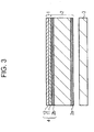
- Fig. 3 shows one example of the structure of a liquid crystal display apparatus according to a first embodiment of the present invention.
- the liquid crystal display apparatus includes a backlight 3 that emits light and a liquid crystal panel 2 that temporally and spatially modulates light emitted from the backlight 3 to display an image.
- Polarizers 2a and 2b are respectively provided on two surfaces of the liquid crystal panel 2.
- An antiglare film 1 is provided on the polarizer 2b provided at the display surface side of the liquid crystal panel 2.
- the polarizer 2b having the antiglare film 1 or an antiglare layer on one main surface thereof is referred to as an antiglare polarizer 4.
- the backlight 3 includes, for example, a light source, a reflecting plate, an optical film, and the like.
- a cold cathode fluorescent lamp (CCFL), a hot cathode fluorescent lamp (HCFL), an organic electroluminescence (OEL), an inorganic electroluminescence (IEL), a light emitting diode (LED), or the like is used as the light source.
- Examples of the display mode that can be used for the liquid crystal panel 2 include a twisted nematic (TN) mode, a super twisted nematic (STN) mode, a vertically aligned (VA) mode, an in-plane switching (IPS) mode, an optically compensated birefringence (OCB) mode, a ferroelectric liquid crystal (FLC) mode, a polymer dispersed liquid crystal (PDLC) mode, and a phase change guest host (PCGH) mode.
- TN twisted nematic
- STN super twisted nematic
- VA vertically aligned
- IPS in-plane switching
- OBC optically compensated birefringence
- FLC ferroelectric liquid crystal
- PDLC polymer dispersed liquid crystal
- PCGH phase change guest host
- the polarizers 2a and 2b are respectively provided on two surfaces of the liquid crystal panel 2 so that transmission axes thereof are orthogonal to each other, for example.
- Each of the polarizers 2a and 2b allows only one of orthogonal polarized components of incident light to pass and blocks the other component by absorption.
- Each of the polarizers 2a and 2b may be a uniaxially stretched hydrophilic polymer film such as a polyvinyl alcohol film, a partially formalized polyvinyl alcohol film, an ethylenevinyl acetate copolymer partially saponified film, or the like, with a dichroic substance, such as iodine or a dichroic dye, adsorbed thereto.
- an image clarity measuring device includes a light source 31, a slit 32, a lens 33, another lens 35, an optical comb 36, and a photoreceiver 37.
- a specimen 34 (for example, the antiglare film 1), which is an object to be measured, is disposed between the lens 33 and the lens 35.
- the slit 32 is disposed at the focal position of the lens 33, and the optical comb 36 is disposed at the focal position of the lens 35.
- Optical combs having comb widths of, for example, 2 mm, 1 mm, 0.5 mm, 0.25 mm, and 0.125 mm are provided as the optical comb 36.
- An appropriate optical comb is selected from these optical combs 36 and used.
- light emitted from the light source 31 is extracted as an artificial line light source through the slit 32 and is allowed to pass through the lens 33 so that the light is perpendicularly transmitted through the specimen 34 as parallel light.
- the light is then focused again using the lens 35, and the light that has passed through the optical comb 36 is received with the photoreceiver 37.
- the contrast between brightness and darkness is determined by calculations.
- light is focused to the size of the slit 32 at the portion of the optical comb 36.
- the quantity of light received is 100% at a position corresponding to the transparent portion of the optical comb 36 and 0% at a position corresponding to the non-transparent portion of the optical comb 36.
- the image of the slit 32 focused on the optical comb 36 becomes wide because of the effect of the blurring. Consequently, two ends of the image of the slit 32 overlap the non-transparent portions at a position corresponding to the transparent portion, and thus the quantity of light decreases from 100%.
- the quantity of light increases from 0%.
- the transmitted image clarity values measured with optical combs having comb widths of 1 mm, 0.5 mm, 0.25 mm, and 0.125 mm are referred to as "value C(1.0) at a 1-mm comb width", “value C(0.5) at a 0.5-mm comb width”, “value C(0.25) at a 0.25-mm comb width”, and “value C(0.125) at a 0.125-mm comb width", respectively, as needed.
- the transmitted image clarity value C measured in accordance with JIS-K7105 is set as follows whereby good contrast is achieved for fine images and highly clear images are obtained while having an antiglare property.
- the value C(0.125) at a 0.125-mm comb width" of the antiglare film 1 is 45 or more and 100 or less, preferably 55 or more and 98 or less, and most preferably 65 or more and 98 or less.
- a ratio of the value C(0.125) at a 0.125-mm comb width to the value C(2.0) at a 2-mm comb width of the antiglare film 1, i.e., ([C(0.125)/C(2.0)] ⁇ 100), is preferably 50% or more and 100% or less, more preferably 65% or more and 100% or less, and most preferably 80% or more and 100% or less.
- the ratio ([C(0.125)/C(2.0)] ⁇ 100) obtained as a measured value may exceed 100, but in such cases, the ratio is considered to be 100.
- the feeling of roughness of the reflected image can be suppressed by controlling the ratio to 50% or more.
- a small ratio between these two values means that, when the surface is macroscopically observed (to an extent that can resolve 2.0 mm) and when the surface is microscopically observed (to an extent that can resolve 0.125 mm), the roughness is different from each other. In such a case, the possibility that local protrusions are formed is high, and an image appears rough when the image is reflected at such a surface.
- a display with a feeling of a high contrast can be obtained for any types of images by controlling the sum to the above ranges.
- the value measured using a comb having a large width is not significantly lower than the value measured using a comb having a small width. Accordingly, in the case where the sum is 220, the transmitted image clarity at a 2.0-mm width is 55 at the minimum. At a contrast value lower than this, the image appears blurred.
- Fig. 5A shows a display of a black and white image, and an edge portion E shown by the arrow indicates a boundary between white and black of the image.
- Fig. 5B shows luminance curves of transmitted images. The luminance curves f to i in Fig. 5B represent the luminance curves below, respectively.
- Luminance curve f A luminance curve obtained when a black and white image is displayed on a screen on which no antiglare film is provided
- Luminance curve h A luminance curve obtained when a black and white image is displayed on a screen on which a conventional antiglare film is provided
- Luminance curves g and i Luminance curves each obtained when a black and white image is displayed on a screen on which the antiglare film 1 of the first embodiment is provided.
- the conventional antiglare film is the antiglare film 101 shown in Fig. 1 .
- luminance line curve f In the case where no antiglare film is provided on the display screen, as shown in luminance line curve f, the luminance drastically changes at the edge portion E of the black and white image, and the curve is steep. Thus, when the display screen is observed, a viewer feels that the contrast of the black and white image is very high.
- the antiglare film 101 is provided on the display screen, as shown in luminance curve h, the luminance does not drastically change at the edge portion E, and the curve is gentle. Thus, the edge is not clear and a problem that an image appears blurred occurs.
- the value C(2.0) at a 2-mm comb width which is a relatively large comb width
- the value C(0.125) at a 0.125-mm comb width which is a relatively small comb width
- the antiglare film 1 according to the first embodiment of the present invention is provided on the display screen, as shown in luminance curve g or i, the luminance gently changes at portions other than the edge portion E, but the luminance drastically changes at the edge portion E. Accordingly, even when the portions other than the edge portion E is somewhat blurred, the viewer can feel that the contrast is high. Consequently, even when the optical comb width is somewhat changed, the difference in the transmitted image clarity value C is small, and the ratio C(0.125)/C(2.0) of the value C(0.125) at a 0.125-mm comb width to the value C(2.0) at a 2-mm comb width is 0.5 or more.
- a feature is defined as a ratio of the value C(0.125) at a 0.125-mm comb width to the value C(2.0) at a 2-mm comb width. This feature means that the transmitted image clarity does not significantly change between a large pitch and a small pitch.
- the antiglare film 1 of the first embodiment is excellent in terms of clarity at a smaller pitch than that of conventional one, a fine image can be displayed more clearly to emphasize the edge, and an image having a high contrast can be obtained.
- the surface haze is preferably as low as possible, and most preferably zero.
- a completely flat surface causes a problem in that a reflected image is clearly observed.
- both reflection and black floating can be prevented by providing a smooth wave profile that cannot be measured as a surface haze.
- a TAC film was bonded to a surface of the film with an optical tackiness agent therebetween to measure the haze.
- the measured value was larger than the haze of the optical film of the present invention alone, but the reason for this is not clear. Accordingly, although the surface haze was negative values in terms of calculation, the negative surface haze was considered to be zero in the present invention. Note that it was confirmed that the haze of a TAC with another TAC bonded on a surface thereof with an optical tackiness agent therebetween was 0.5% or less.
- a feature of the optical film of the present invention lies in that when the 20° glossiness of the optical film of the present invention is the same as that of a conventional optical film, the 60° glossiness of the optical film of the present invention is higher than that of the conventional optical film.
- Ordinary display apparatuses are hardly observed from a high angle and are often observed from a low angle of about 20°, i.e., from a substantially perpendicular direction. Therefore, in order to suppress a reflected image, it is preferable that the 20° glossiness be low.
- specular reflection of external light incident from a direction of 60° is low, that is, diffuse reflection increases.
- the inventors of the present invention conducted extensive studies on the relationship between the 20° glossiness and 60° glossiness.
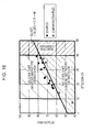
- Gs(20°) and Gs(60°) preferably satisfy the relationship represented by formula (1) below: G ⁇ s 60 ⁇ ° > G ⁇ s 20 ⁇ ° ⁇ 0.75 + 48 (wherein Gs(20°) is preferably in the range of Gs(20°) ⁇ 40, and more preferably in the range of 10 ⁇ Gs(20°) ⁇ 40.)
- the 20° glossiness is preferably low, and specifically, preferably 40 or less, more preferably 35 or less, and further preferably 30 or less. This is because a reflected image can be suppressed as described above by controlling the 20° glossiness to the above ranges.
- the opacity is preferably 1.0 or less, and more preferably 0.8 or less.
- the 20° glossiness Gs(20°) and the 60° glossiness Gs(60°) preferably satisfy the relationship represented by formula (2) below: G ⁇ s 60 ⁇ ° > G ⁇ s 20 ⁇ ° ⁇ 0.25 + 72 (wherein Gs(20°) is preferably in the range of 40 ⁇ Gs(20°) ⁇ 80, more preferably in the range of 50 ⁇ Gs(20°) ⁇ 70, and further preferably in the range of 50 ⁇ Gs(20°) ⁇ 65.)
- Fig. 6 is an enlarged cross-sectional view showing one example of the structure of an antiglare film 1 according to the first embodiment of the present invention.
- the antiglare film 1 includes a base member 11 and an antiglare layer 12 provided on the base member 11.
- the antiglare layer 12 contains fine particles 13, and fine irregularities are formed on the surface of the antiglare layer 12.
- the average film thickness of the antiglare layer is preferably 8 ⁇ m or more and 25 ⁇ m or less, more preferably 9 ⁇ m or more and 18 ⁇ m or less, and further preferably 10 ⁇ m or more and 14 ⁇ m or less.
- the average film thickness is 8 ⁇ m or more, a sufficient hardness can be achieved.
- the average film thickness is 25 ⁇ m or less, significant curling may occur in the production process.
- the antiglare film can be formed into a polarizing plate by constructing a special line equipped with a pass-roll that can correct the curling as a line for forming a polarizing plate in the subsequent step.
- the average film thickness is 18 ⁇ m or less, curling may occur to some degree in the production process.
- the antiglare film can be formed into a polarizing plate without preparing the above special line for the subsequent step.
- the average film thickness is 14 ⁇ m or less, curling hardly occurs in the production process and a high-quality polarizer or the like can be provided.
- the average particle diameter of the fine particles 13 is 2 ⁇ m or more and 8 ⁇ m or less, more preferably 4 ⁇ m or more and 8 ⁇ m or less, and further preferably 5 ⁇ m or more and 8 ⁇ m or less.
- the reason for this is as follows. If the average particle diameter is less than 2 ⁇ m, the fine particles 13 may remain as aggregated particles in the coating material because dispersion of the fine particles 13 is difficult to achieve. Accordingly, even when the film thickness is adjusted, it is difficult to control an adequate surface profile. If the average particle diameter exceeds 8 ⁇ m, glare cannot be suppressed when the fine particles 13 are used in a high-definition display. Note that, in the present invention, the average particle diameter of the fine particles 13 is measured by a pore electrical resistance method.
- the amount of fine particles 13 added is preferably 8 parts by weight or more and 50 parts by weight or less, more preferably 10 parts by weight or more and 30 parts by weight or less, and further preferably 10 parts by weight or more and 20 parts by weight or less per 100 parts by weight of the total amount of the resin. If the amount of fine particles 13 added is less than 8 parts by weight, sparseness and denseness of the fine particles 13 in the in-plane direction become clearly identified. Accordingly, the roughness increases and a clear image cannot be obtained.
- the amount of fine particles 13 added exceeds 50 parts by weight, the haze increases, the value of image clarity decreases, and the image contrast of the display apparatus also decreases as a result.
- scattering of light can be suppressed by decreasing the difference in refractive index between the fine particles 13 and the matrix. Therefore, the amount of fine particles 13 added and the difference in refractive index between the fine particles 13 and the matrix resin are preferably adjusted in accordance with the desired image contrast.
- the difference in refractive index between the fine particles 13 and the matrix is preferably 0.03 or less and more preferably 0.02 or less.
- acrylic particles, fine particles containing an acryl/styrene copolymer as a main component, and styrene particles can be used as the organic fine particles.
- fine particles containing an acryl/styrene copolymer as a main component are preferable, and fine particles containing, as a main component, an acryl/styrene copolymer having a refractive index of 1.50 to 1.56 are particularly preferable. This is because the fine particles 13 can be distributed densely in some regions and sparsely in other regions.
- the particle distribution formed during drying can also be controlled by hydrophilizing or hydrophobizing the surfaces of the fine particles.
- fine particles 13 In the case where slightly polarized fine particles, such as acrylic resin fine particles, are used as the fine particles 13, convection in the coating material that occurs during drying decreases. Thus, the fine particles are dispersed and a desired particle distribution is difficult to form. To overcome this problem, a solvent having a high surface tension must be used. However, such a solvent has a high boiling point and the resulting coating film is not readily dried, resulting in difficulty of handling during manufacturing. Accordingly, fine particles in which a nonpolar resin, such as styrene, is blended are preferably used. As for fine particles containing an acryl/styrene copolymer as a main component, the surface energy can be changed by changing the composition ratio of the acryl and styrene in synthesis.
- a nonpolar resin such as styrene
- fine particles containing acryl/styrene copolymers as main components those having a mixing ratio that achieves a refractive index of 1.50 to 1.56 are preferable, and those having a mixing ratio that achieves a refractive index of 1.505 to 1.545 are particularly preferable. This is because a desired particle distribution can be achieved, and a desired surface profile can be obtained by adding a process of controlling cure shrinkage.
- a ratio ((D/T) ⁇ 100) of the average particle diameter D of the fine particles to the average film thickness T of the antiglare layer is 20% or more and 70% or less. The reason for this is as follows. If the ratio is less than 20%, the surface readily becomes flat and it is difficult to control an adequate wave profile. If the ratio exceeds 70%, the fine particles 13 protrude from the surface, thus increasing opacity.
- a film, sheet, or substrate having transparency can be used as the base member 11.
- known polymer materials can be used as the material for the base member 11.
- the known polymer materials include triacetyl cellulose (TAC), polyesters (TPEE), polyethylene terephthalate (PET), polyimides (PI), polyamides (PA), aramids, polyethylene (PE), polyacrylates, polyethersulfone, polysulfone, polypropylene (PP), diacetyl cellulose, polyvinyl chloride, acrylic resins (PMMA), polycarbonate (PC), epoxy resins, urea resins, urethane resins, and melamine resins.
- the thickness of the base member 11 is preferably 38 ⁇ m to 100 ⁇ m from the standpoint of productivity but is not particularly limited to this range.
- the base member 11 preferably has a function as a protective film of the polarizer 2b. This is because a protective film need not be separately provided on the polarizer 2b, and thus the thickness of the polarizer 2b having the antiglare film 1 can be reduced.
- the method for manufacturing the antiglare film 1 includes applying a coating material containing fine particles 13, a resin, and a solvent onto a base member 11, drying the solvent, and then curing the resin.
- a resin, fine particles 13, and a solvent are mixed in a stirrer, such as a disper, or a dispersion machine, such as a bead mill, to obtain a coating material in which the file particles 13 are dispersed.
- a photostabilizer, an ultraviolet absorber, an antistatic agent, a flame retardant, an antioxidant, and the like may be added, if necessary.
- silica fine particles or the like may further be added as a viscosity modifier.
- an organic solvent that dissolves the resin material used, that has good wettability with the fine particles 13, and that does not bleach the base member 11 can be used as the solvent.
- the organic solvent include tertiary butanol, isopropyl acetate, and the like.
- the resin contains a polymer and an oligomer and/or monomer, preferably contains a polymer and an oligomer. Specifically, the resin contains 3% by weight or more and 20% by weight or less polymer and 80% by weight or more and 97% by weight or less oligomer and/or monomer, and more preferably contains 5% by weight or more and 15% by weight or less polymer and 85% by weight or more and 95% by weight or less oligomer and/or monomer.
- the polymer is added in order to adjust cure shrinkage.
- the cure shrinkage is large, and the surface is roughened, the root-mean-square slope R ⁇ q and the arithmetic mean roughness Ra are increased, and the opacity is increased.
- the ratio of substances that inhibit curing in the resin increases and the viscosity of the coating material increases.
- the dispersibility of the fine particles 13 is degraded, and sparseness and denseness of the fine particles 13 become clearly identified more than necessary.
- the difference in cure shrinkage notably appears between the sparse portions and the dense portions, thereby increasing the opacity.
- a decrease in the hardness of the antiglare layer 12 becomes also significant.
- the Martens hardness of the antiglare layer 12 is preferably 220 N/mm 2 or more.
- the polymer is added in an amount more than 20 parts by weight, it is difficult to achieve a Martens hardness of 220 N/mm 2 or more.
- the Martens hardness is determined by the following evaluation method.
- An antiglare layer 12 is formed on a base member 11. A portion where no fine particles 13 are present is selected, and a surface hardness is measured by an indentation method under the conditions below.
- Measuring device PICODENTOR HM-500 (Fischer Instruments K.K.) Indenter: Vickers indenter Maximum indentation depth: 10% or less of the thickness of the coating film (the thickness of the AG layer)
- the resin is preferably an ionizing radiation-curable resin that is cured by ultraviolet rays or electron beams or a thermosetting resin that is cured by heat.
- a photosensitive resin that can be cured by ultraviolet rays is most preferable.
- examples of such a photosensitive resin include acrylate resins such as urethane acrylates, epoxy acrylates, polyester acrylates, polyol acrylates, polyether acrylates, and melamine acrylates.
- a resin that exhibits a good light-transmitting property in view of a good image-transmitting property and a resin that has a high hardness in view of scratch resistance are particularly preferable.
- Such a resin can be appropriately selected.
- the ionizing radiation-curable resin is not particularly limited to ultraviolet-curable resins, and any ionizing radiation-curable resin having a light-transmitting property can be used. However, a resin that does not cause a significant change in the hue of transmitted light and the amount of transmitted light due to coloring and haze is preferable.
- Such a photosensitive resin can be obtained by blending a photopolymerization initiator with organic materials, such as monomers, oligomers, and polymers, which can form the resin.
- organic materials such as monomers, oligomers, and polymers, which can form the resin.
- a urethane acrylate resin is produced by allowing a polyester polyol to react with an isocyanate monomer or prepolymer and then allowing the resulting reaction product to react with a hydroxyl-group-containing acrylate or methacrylate monomer.
- photopolymerization initiator contained in the photosensitive resin examples include benzophenone derivatives, acetophenone derivatives, and anthraquinone derivatives. These may be used alone or in combinations.
- a component that improves coating film formation e.g., an acrylic resin, may further be appropriately selected and blended with the photosensitive resin.
- a urethane resin, an acrylic resin, a methacrylic resin, a styrene resin, a melamine resin, or a cellulosic resin that can be fixed at least by drying, an ionizing radiation-curable oligomer, or a thermosetting oligomer can be appropriately mixed with photosensitive resin and used.
- the hardness and curling of the antiglare layer 12 can be adjusted by appropriately mixing such resins.
- These resins are not limited thereto.
- a polymer that has an ionizing radiation-sensitive group, such as an acrylic double bond, or a thermosetting group, such as an - OH group can be used.
- the coating material obtained as described above is applied onto the base member 11.
- the coating material is applied so that the average film thickness after drying is preferably 8 ⁇ m or more and 25 ⁇ m or less, more preferably 9 ⁇ m or more and 18 ⁇ m or less, and further preferably 10 ⁇ m or more and 14 ⁇ m or less. This is because a sufficient hardness is not achieved at an excessively small average film thickness, and curling occurs in the step of curing the resin during manufacturing at an excessively large average film thickness.
- the application method is not particularly limited and any known application method can be employed.
- Examples of the known application methods include a micro-gravure coating method, a wire-bar coating method, a direct gravure coating method, a die coating method, a dipping method, a spray coating method, a reverse roll coating method, a curtain coating method, a comma coating method, a knife coating method, and a spin-coating method.
- drying and curing are conducted to obtain an antiglare layer 12.
- an irregular shape that has a longer period and is gentle i.e., a root-mean-square slope R ⁇ q that is adequately small
- individual fine particles 13 are not uniformly dispersed but are intentionally distributed densely in some portions and sparsely in other portions by the convection during drying.
- a portion where the fine particles 13 are densely gathered forms one peak, and thus a surface profile having smooth waves is formed.
- the drying temperature and the drying time can be appropriately determined on the basis of the boiling point of the solvent contained in the coating material. In such a case, the drying temperature and the drying time are preferably set in the ranges where deformation of the base member 11 due to thermal shrinkage does not occur in consideration of heat resistance of the base member 11.
- the drying step and curing step will be specifically described below.
- the coating material applied on the base member 11 is dried at a predetermined temperature to generate convection in the coating material and to distribute the fine particles 13 densely in some regions and sparsely in other regions by the convection.
- the degree of distribution of the fine particles 13, the distribution including sparse portions and dense portions, can be selected, for example, by appropriately adjusting the surface tension of the solvent and the surface energy of the fine particles 13.
- the drying temperature and the drying time can be appropriately set on the basis of the boiling point of the solvent contained in the coating material. In such a case, the drying temperature and the drying time are preferably set in the ranges where deformation of the base member 11 due to thermal shrinkage does not occur in consideration of heat resistance of the base member 11.
- the drying conditions are not particularly limited.
- the drying may be natural drying or artificial drying in which the drying temperature and the drying time are adjusted.
- wind ripples do not form on the surface of the coating film. The reason for this is as follows. If wind ripples are formed, the desired gently wavy irregular shape does not tend to be formed on the surface of the antiglare layer, and thus it becomes difficult to achieve both the antiglare property and the contrast.
- the resin dried on the base member 11 is cured by, for example, irradiation of ionizing radiation or heating.
- gentle irregularities are formed on the surface of the coating material because of the difference in cure shrinkage ratio between the portions where the fine particles 13 are densely distributed and the portions where the fine particles 13 are sparsely distributed. That is, a portion where the fine particles 13 are densely distributed forms one peak, and thus waves having a large period are formed. That is, an irregular shape that has a longer period and is gentle as compared with that of a conventional antiglare layer is formed on the surface of the antiglare layer 12.
- the ionizing radiation can be used as the ionizing radiation.
- Ultraviolet rays are preferable from the standpoint of production equipment.
- the ultraviolet ray source that can be used include an ultra-high-pressure mercury lamp, a high-pressure mercury lamp, a low-pressure mercury lamp, a carbon arc, a xenon arc, and a metal halide lamp.
- the integrated exposure dose is adequately selected in consideration of the curing properties of the resin, suppression of yellowing of the resin and the base member 11, and the like.
- the atmosphere of irradiation include air and an inert gas atmosphere such as nitrogen or argon.
- the antiglare layer 12 is obtained by applying the fine particles 13 and the resin onto the base member 11, distributing the fine particles 13 densely in some regions and sparsely in other regions, and conducting curing so that the coating material in the regions where the fine particles 13 are sparsely distributed is significantly shrunk compared with the coating material in the regions where the fine particles 13 are densely distributed.
- the resin contains 3% by weight or more and 20% by weight or less polymer and 80% by weight or more and 97% by weight or less oligomer and/or monomer
- the fine particles 13 are organic fine particles having an average particle diameter of 2 ⁇ m or more and 8 ⁇ m or less
- the ratio ((D/T) ⁇ 100) of the average particle diameter D of the fine particles 13 to the average film thickness T is 20% or more and 70% or less.
- the transmitted image clarity value measured with an optical comb having a width of 0.125 mm is 45 or more. Accordingly, the antiglare film 1 having good antiglare property and transmitted image clarity can be obtained.
- Fig. 7 shows one example of the structure of an antiglare film according to a second embodiment of the present invention.
- an antiglare film 1 of this second embodiment differs from the first embodiment in that a low-refractive-index layer 14 is further provided on an antiglare layer 12. Since a base member 11 and the antiglare layer 12 are the same as those in the first embodiment, they are assigned the same reference characters and a description thereof is omitted.
- the low-refractive-index layer 14 is preferably provided so as to follow the waves on the surface of the antiglare layer. More preferably, the low-refractive-index layer 14 has a substantially uniform thickness, and the waves of the surface of an antireflection layer have gentle waves substantially the same as those of the surface of the antiglare layer. According to this structure, even when the low-refractive-index layer 14 is provided, both contrast and antiglare property can be achieved. Note that, although it is ideal that the low-refractive-index layer 14 have a substantially uniform thickness as described above, the low-refractive-index layer 14 need not be provided over the entire region of the antiglare layer 12. A sufficient contrast can be achieved as long as the low-refractive-index layer is substantially uniformly provided over the most portions of the antiglare layer 12 excluding the protruding portions, that is, over relatively flat and smooth portions having a high reflectivity.
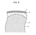
- Fig. 8 is an enlarged cross-sectional view of the low-refractive-index layer 14 shown in Fig. 7 .
- the low-refractive-index layer 14 includes, for example, a resin and hollow fine particles 15.
- the hollow fine particles 15 are preferably dispersed over the entire surface of the antiglare layer 12.
- the hollow fine particles 15 are embedded in the low-refractive-index layer 14, and the embedded hollow fine particles 15 form a layer of the hollow fine particles 15 in which about two to three particles are overlapped in the thickness direction of the low-refractive-index layer 14.
- This method for manufacturing the antiglare film of the second embodiment differs from the first embodiment in that the method further includes a step of forming the low-refractive-index layer, the step being conducted after the step of forming the antiglare layer. Accordingly, only the step of forming the low-refractive-index layer will be described below.
- hollow fine particles 15, a resin, and a solvent are mixed in a stirrer, such as a disper, or a dispersion machine, such as a bead mill, to prepare a coating material.
- a stirrer such as a disper, or a dispersion machine, such as a bead mill
- additives such as a photostabilizer, an ultraviolet absorber, an antistatic agent, a flame retardant, an antioxidant, and the like may be added, if necessary.
- an ionizing radiation-curable resin that can be cured by irradiation of light, an electron beam, or the like and a thermosetting resin that can be cured by heat can be used alone or in combinations. From the standpoint of ease of manufacturing, a photosensitive resin that can be cured by ultraviolet rays is most preferable.
- the ionizing radiation-curable resin preferably contains 90% or more of a polyfunctional monomer. Examples of the polyfunctional monomer include esters of a polyhydric alcohol and (meth)acrylic acid.
- examples thereof include ethylene glycol di(meth)acrylate, 1,4-dicyclohexane diacrylate, pentaerythritol tetra(meth)acrylate, pentaerythritol tri(meth)acrylate, trimethylolpropane tri(meth)acrylate, trimethylolethane tri(meth)acrylate, dipentaerythritol tetra(meth)acrylate, dipentaerythritol penta(meth)acrylate, dipentaerythritol hexa(math)acrylate, 1,2,3-cyclohexane tetramethacrylate, polyurethane polyacrylate, and polyester polyacrylate.
- the hollow fine particles 15 include inorganic fine particles such as silica and alumina, and organic fine particles such as styrene and acryl. Silica fine particles are particularly preferable. Since the hollow fine particles 15 contain air inside, the refractive index thereof is lower than that of normal fine particles. For example, whereas the refractive index of silica fine particles is 1.46, the refractive index of hollow silica fine particles is 1.45 or less.
- the average particle diameter of the hollow fine particles 15 is preferably 10 to 200 nm and more preferably 30 to 60 nm. If the average particle diameter exceeds 200 nm, the size is not negligible compared with the visible light wavelength, and thus light is scattered on the surface of the low-refractive-index layer 14. As a result, the transparency is degraded and a display surface and the like appear whitish. If the average particle diameter is less than 10 nm, the hollow fine particles 15 tend to aggregate. Furthermore, from the standpoint of improving the compatibility with the resin, the hollow fine particles 15 such as hollow silica fine particles preferably have (meth)acryloyl groups polymerizable with an ionizing radiation on the surfaces thereof.
- modified silicon acrylate compounds or the like may be used as the additive.
- Specific examples thereof include compounds having at least one organic group in a dimethyl silicon molecule.
- the equivalent of the organic group bonded to dimethyl silicon is preferably 1,630 g/mol or more.
- the equivalent of the organic group can be calculated using a nuclear magnetic resonance (NMR) measuring method from the peak intensity ratio of 1 H of the methyl groups and 1 H of the organic group in the dimethyl silicon molecule.
- NMR nuclear magnetic resonance
- the organic group include a methacryl group, an acryl group, and a mercapto group.
- a solvent that dissolves the resin used but that does not dissolve the underlying antiglare layer 12 is preferred as the solvent.
- a solvent include organic solvents such as tertiary butanol, toluene, methyl ethyl ketone (MEK), isopropyl alcohol (IPA), and methyl isobutyl ketone (MIBK) .
- the coating material prepared as described above is applied onto the antiglare layer 12.
- the method of applying the coating material include a gravure coater, a bar coater, a die coater, a knife coater, a comma coater, a spray coater, and a curtain coater. It should be noted that the application method is not limited to those described above and any method can be employed as long as a coating material can be uniformly applied so as to have a predetermined thickness.
- the coating material applied on the antiglare layer 12 is dried and cured. Consequently, a low-refractive-index layer 14 with a gentle irregular shape is formed on the antiglare layer 12.
- the drying and curing methods the same as those used in the above-described process of preparing the antiglare layer of the first embodiment can be employed.
- the reflectivity can be further decreased compared with the first embodiment described above.
- Fig. 9 shows one example of the structure of an antiglare film according to a third embodiment of the present invention.
- an antiglare film 1 differs from the above-described first embodiment in that a multilayered antireflection layer is provided on an antiglare layer 12. Since a base member 11 and the antiglare layer 12 are the same as those in the above-described first embodiment, they are assigned the same reference characters and a description thereof is omitted.
- a multilayered antireflection layer 16 is a stacked film including both low-refractive-index layers 16L and high-refractive-index layers 16H.
- the number of stacks of the low-refractive-index layers 16L and the number of stacks of the high-refractive-index layers 16H are adequately selected in accordance with desired characteristics.
- the material for the low-refractive-index layers 16L that can be used include, but are not particularly limited to, SiO x , SiO 2 , Al 2 O 3 , and mixtures thereof.
- the material can be adequately selected from known low-refractive-index materials in accordance with characteristics required for the low-refractive-index layers 16L and used.
- Examples of the material for the high-refractive-index layers 16H that can be used include, but are not particularly limited to, TiO 2 Nb 2 O 5 , Ta 2 O 5 , WO 3 , and mixtures thereof.
- the material can be adequately selected from known high-refractive-index materials in accordance with characteristics required for the high-refractive-index layers 16H and used.
- a sputtering method is preferably used as a method for depositing the low-refractive-index layers 16L and the high-refractive-index layers 16H, but the method is not limited to this.
- an antifouling layer 17 may be further provided on the multilayered antireflection layer 16, as required.
- a fluorine-based compound is preferably used as the antifouling layer 17, but the antifouling layer 17 is not limited thereto.
- the reflectivity can be further decreased compared with the first embodiment described above.
- an optical film used as an antiglare film in the first embodiment is used as an "anti-Newton ring (ANR) film” (hereinafter referred to as "ANR film”).
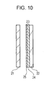
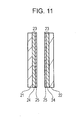
- Figs. 10 and 11 show examples of the structures of display apparatuses according to the fourth embodiment of the present invention.
- Each of the display apparatuses includes a display unit 21 and a front surafce member 22 provided at the front surface side of the display unit 21.
- an air layer is formed between the display unit 21 and the front surafce member 22.
- An ANR film 23 is provided on at least one of the front surface side of the display unit 21 and the rear surface side of the front surafce member 22.
- Fig. 10 shows an example of a display apparatus including an ANR film 23 on the rear surface side of the front surafce member 22.
- Fig. 10 shows an example of a display apparatus including an ANR film 23 on the rear surface side of the front surafce member 22.
- ANR films 23 both on the front surface side of the display unit 21 and on the rear surface side of the front surafce member 22.
- ANR films 23 are preferably provided both on the display surface side of the display unit 21 and on the rear surface side of the front surafce member 22.
- the ANR film 23 is bonded to the front surafce member 22 or the display unit 21 with an adhesive agent or the like.
- the "front surface” is the surface serving as a display surface, i.e., the surface located at the viewer's side, and the "rear surface” is the surface opposite the display surface.
- Examples of the display unit 21 that can be used include liquid crystal displays, cathode ray tube (CRT) displays, plasma display panels (PDPs), organic electroluminescence (EL) displays, inorganic EL displays, surface-conduction electron-emitter displays (SEDs), and field emission displays (FEDs).
- LCD cathode ray tube
- PDP plasma display panels
- EL organic electroluminescence
- EL inorganic EL displays
- SEDs surface-conduction electron-emitter displays
- FEDs field emission displays
- the front surafce member 22 is used for the purpose of providing mechanical, thermal, and weathering protections and a design function to the front surface (viewer's side) of the display unit 21.
- the front surafce member 22 is, for example, sheet-shaped, film-shaped, or plate-shaped.
- Examples of the material for the front surafce member 22 that can be used include, glass, triacetyl cellulose (TAC), polyesters (TPEE), polyethylene terephthalate (PET), polyimides (PI), polyamides (PA), aramids, polyethylene (PE), polyacrylates, polyethersulfone, polysulfone, polypropylene (PP), diacetyl cellulose, polyvinyl chloride, acrylic resins (PMMA), and polycarbonate (PC).
- TAC triacetyl cellulose
- TPEE polyesters
- PET polyethylene terephthalate
- PI polyimides
- PA polyamides
- PE polyacrylates
- polyethersulfone polysulfone
- PP polypropylene
- PC polycarbonate
- the material is not particularly limited to these materials and any material having transparency can be used.
- Fig. 12 shows one example of the structure of an ANR film.
- An ANR film 23 suppresses occurrence of Newton rings in the display apparatus.
- the ANR film 23 includes a base member 24 and an ANR layer 25 provided on the base member 24.
- the ANR film 23 is bonded onto an adherend such as a front surafce member 22 with an adhesive layer 26 therebetween.
- the adhesive layer 26 contains an adhesive agent as a main component.
- known adhesive agents used in the technical field of optical films can be used as the adhesive agent.
- tackiness agents such as pressure-sensitive adhesives (PSAs) are also considered as one type of adhesive agents.
- PSAs pressure-sensitive adhesives
- a film identical to the antiglare film 1 in the first embodiment can be used as the ANR film 23.
- the base member 24 and the ANR layer 25 identical to the base member 11 and the antiglare layer 12, respectively, in the first first embodiment can be used.
- an antireflection (AR) layer 27 is further formed on the ANR layer 25 from the standpoint of reducing reflected light.
- the AR layer 27 may be either a dry-type layer or a wet-type layer, but is preferably a wet-type layer.
- Examples of the wet-type AR layer 27 include a layer containing a fluorine-based resin and a layer containing hollow fine particles such as silica.
- the occurrence of Newton rings can be suppressed or the occurrence of Newton rings can be reduced to a negligible level.
- Figs. 13 and 14 show examples of the structures of display apparatuses according to a fifth embodiment of the present invention.
- This fifth embodiment differs from the fourth embodiment in that the display apparatus includes a display unit 21, a rear surafce member 26 provided at the rear surface side of the display unit 21, and an ANR film 23 provided on at least one of the rear surface side of the display unit 21 and the front surface side of the rear surafce member 26.
- Fig. 13 shows an example of a display apparatus including an ANR film 23 on the rear surface side of the display unit 21.
- Fig. 14 shows an example of a display apparatus including an ANR film 23 on the rear surface side of the display unit 21 and on the front surface side of the rear surafce member 26, respectively. Note that the same components as the fourth embodiment are assigned the same reference characters and a description thereof is omitted.
- the rear surafce member 26 is, for example, sheet-shaped, film-shaped, or plate-shaped.
- the rear surafce member 26 is, for example, a diffusing plate or diffusing sheet that makes the illuminance of light emitted from a light source uniform in a plane, a lens film for controlling the viewing angle, a polarization separation reflection film that polarizes and separates light from the light source for reuse, or the like.
- the occurrence of Newton rings can be suppressed or the occurrence of Newton rings can be reduced to a negligible level.
- Fig. 15 shows one example of the structure of a display apparatus according to a sixth embodiment of the present invention.
- This sixth embodiment differs from the fourth embodiment in that an ANR layer 25 is formed directly on at least one of the front surface side of the display unit 21 and the rear surface side of the front surafce member 22 without using an adhesive agent or the like.
- Fig. 15 shows an example in which the ANR layer 25 is formed directly on the rear surface side of the front surafce member 22.
- the same components as the fourth embodiment are assigned the same reference characters and a description thereof is omitted.
- the ANR layer 25 may be formed directly on at least one of the rear surface side of the display unit 21 and the front surface side of the rear surafce member 26.
- the ANR layer 25 is formed directly on at least one of the front surface side of the display unit 21 and the rear surface side of the front surafce member 22, the structure and the production process of the display apparatus can be simplified compared with the fourth embodiment.
- the average particle diameter of fine particles and the dry film thickness of an antiglare layer were measured as follows.
- the average particle diameter of fine particles was determined by measuring the particle diameter with a Coulter Multisizer and averaging the obtained data.
- the dry film thickness (average film thickness) of the antiglare layer was determined with a contact thickness meter (produced by TESA K.K.) as follows.
- a cylindrical probe having a diameter of 6 mm was used as a contact probe.
- the cylindrical probe was brought into contact with the antiglare layer at such a low load that the antiglare layer is not broken.
- measurement was performed at arbitrary five points to determine the average value D A of the total thickness of the antiglare film.
- the thickness of an uncoated portion of the same base member was measured to determine the thickness D B of the base member.
- the value calculated by subtracting the thickness D B of the base member from the average value D A was defined as the thickness of the antiglare layer.
- the thickness of the base member can be measured by preparing a cross section of the antiglare film by a microtome technique or the like.
- the thickness thus measured is a microscopic film thickness, it is preferable to determine the film thickness as the average film thickness as described in the former method.
- Example 1 the materials shown in the coating material composition below were blended, and the resulting mixture was stirred for two hours to obtain a coating material.
- the obtained coating material was applied onto a TAC film (produced by Fujifilm Corporation) having a thickness of 80 ⁇ m with a die coater at a rate of 20 m/min.
- the resulting film was dried in a drying oven at 80°C for two minutes and then irradiated with ultraviolet rays at 500 mJ/cm 2 to form an antiglare layer having a dry film thickness of 10.9 ⁇ m.
- an optical film of Example 1 was obtained.
- Example 2 An optical film of Example 2 was obtained as in Example 1 except that the dry film thickness was controlled to be 11.6 ⁇ m by adjusting the die gap, the flow rate of the coating material being supplied, and the back pressure.
- Example 3 An optical film of Example 3 was obtained as in Example 1 except that the dry film thickness was controlled to be 12.8 ⁇ m by adjusting the die gap, the flow rate of the coating material being supplied, and the back pressure.
- Example 4 An optical film of Example 4 was obtained as in Example 1 except that the dry film thickness was controlled to be 14.4 ⁇ m by adjusting the die gap, the flow rate of the coating material being supplied, and the back pressure.
- Example 5 An optical film of Example 5 was obtained as in Example 1 except that the dry film thickness was controlled to be 16.3 ⁇ m by adjusting the die gap, the flow rate of the coating material being supplied, and the back pressure.
- Example 6 An optical film of Example 6 having a dry film thickness of 13.0 ⁇ m was obtained by die coating as in Example 1 except that the coating material composition described below was used.
- Example 7 An optical film of Example 7 was obtained as in Example 1 except that the film formation rate was controlled to be 30 m/min, and the dry film thickness was controlled to be 10.2 ⁇ m by adjusting the die gap, the flow rate of the coating material being supplied, and the back pressure.
- Example 8 An optical film of Example 8 having a dry film thickness of 10.2 ⁇ m was obtained by die coating as in Example 1 except that the coating material composition described below was used and the application rate was controlled to be 30 m/min.
- Hexafunctional urethane acrylic oligomer 87 parts by weight Acrylic polyol-based polymer 13 parts by weight Initiator Irgacure 184 5 parts by weight Solvent Butyl acetate 65 parts by weight Dimethyl carbonate 53 parts by weight Silicon-based leveling agent 0.05 parts by weight Cross-linking MS beads (Techpolymer produced by Sekisui Plastics Co., Ltd., refractive index 1.515, average particle diameter 5.5 ⁇ m, coefficient of variation 7) 20 parts by weight
- Example 9 An optical film of Example 9 was obtained as in Example 8 except that the dry film thickness was controlled to be 9.4 ⁇ m by adjusting the die gap, the flow rate of the coating material being supplied, and the back pressure.
- Example 10 An optical film of Example 10 having a dry film thickness of 14.3 ⁇ m was obtained by die coating as in Example 1 except that the coating material composition described below was used.
- Hexafunctional urethane acrylic oligomer 82 parts by weight Acrylic-based polymer 18 parts by weight Initiator Irgacure 184 5 parts by weight Solvent Butyl acetate 65 parts by weight Dimethyl carbonate 53 parts by weight Silicon-based leveling agent 0.05 parts by weight Cross-linking MS beads (Techpolymer produced by Sekisui Plastics Co., Ltd., refractive index 1.515, average particle diameter 5.5 ⁇ m, coefficient of variation 7) 25 parts by weight
- Example 11 An optical film of Example 11 having a dry film thickness of 14.1 ⁇ m was obtained by die coating as in Example 1 except that the coating material composition described below was used.
- Hexafunctional urethane acrylic oligomer 82 parts by weight Acrylic polyol-based polymer 18 parts by weight Initiator Irgacure 184 5 parts by weight Solvent Butyl acetate 65 parts by weight Dimethyl carbonate 53 parts by weight Fluorine-based leveling agent 0.5 parts by weight Cross-linking MS beads (Techpolymer produced by Sekisui Plastics Co., Ltd., refractive index 1.515, average particle diameter 5.5 ⁇ m, coefficient of variation 7) 25 parts by weight
- Example 12 the materials shown in the coating material composition below were blended, and the resulting mixture was stirred for two hours to obtain a coating material.
- the obtained coating material was applied onto a TAC film (produced by Fujifilm Corporation) having a thickness of 80 ⁇ m with a micro-gravure coater with 80 lines at a rate of 30 m/min.
- the resulting film was dried in a drying oven at 80°C for two minutes and then irradiated with ultraviolet rays at 500 mJ/cm 2 to form an antiglare layer having a dry film thickness of 22.3 ⁇ m.
- an optical film of Example 12 was obtained.
- Hexafunctional urethane acrylic oligomer 87 parts by weight Acrylic polyol-based polymer 13 parts by weight Initiator Irgacure 184 5 parts by weight Solvent Butyl acetate 59 parts by weight Dimethyl carbonate 49 parts by weight Silicon-based leveling agent 0.05 parts by weight Cross-linking MS beads (Techpolymer produced by Sekisui Plastics Co., Ltd., refractive index 1.515, average particle diameter 5.5 ⁇ m, coefficient of variation 7) 27.5 parts by weight
- Example 13 the materials shown in the coating material composition below were blended, and the resulting mixture was stirred with a magnetic stirrer for one hour to obtain a coating material.
- the obtained coating material was applied onto a TAC film (produced by Fujifilm Corporation) having a thickness of 80 ⁇ m with a wire bar coater.
- the resulting film was dried in a drying oven at 80°C for two minutes and then irradiated with ultraviolet rays at 500 J/cm 2 to form an antiglare layer having a dry film thickness of 17.2 ⁇ m.
- an optical film of Example 13 was obtained.
- Hexafunctional urethane acrylic oligomer 87 parts by weight Acrylic polyol-based polymer 13 parts by weight Initiator Irgacure 184 5 parts by weight Solvent Butyl acetate 59 parts by weight Dimethyl carbonate 49 parts by weight Silicon-based leveling agent 0.05 parts by weight Cross-linking MS beads (Techpolymer produced by Sekisui Plastics Co., Ltd., refractive index 1.525, average particle diameter 5.0 ⁇ m, coefficient of variation 7) 27.5 parts by weight
- Example 14 An optical film of Example 14 having a dry film thickness of 15.3 ⁇ m was obtained with a wire bar coater as in Example 13 except that the coating material composition described below was used.
- Hexafunctional urethane acrylic oligomer 87 parts by weight Acrylic polyol-based polymer 13 parts by weight Initiator Irgacure 184 5 parts by weight Solvent Butyl acetate 59 parts by weight Dimethyl carbonate 49 parts by weight Silicon-based leveling agent 0.05 parts by weight Cross-linking MS beads (Techpolymer produced by Sekisui Plastics Co., Ltd., refractive index 1.505, average particle diameter 5.0 ⁇ m, coefficient of variation 8) 27.5 parts by weight
- Example 15 An optical film of Example 15 having a dry film thickness of 14.6 ⁇ m was obtained with a wire bar coater as in Example 13 except that the coating material composition described below was used.
- Hexafunctional urethane acrylic oligomer 87 parts by weight Acrylic polyol-based polymer 13 parts by weight Initiator Irgacure 184 5 parts by weight Solvent Butyl acetate 59 parts by weight Dimethyl carbonate 49 parts by weight Silicon-based leveling agent 0.05 parts by weight Cross-linking MS beads (Techpolymer produced by Sekisui Plastics Co., Ltd., refractive index 1.505, average particle diameter 5.0 ⁇ m, coefficient of variation 8) 37.5 parts by weight
- Example 16 An optical film of Example 16 having a dry film thickness of 14.1 ⁇ m was obtained with a wire bar coater as in Example 13 except that the coating material composition described below was used.
- Hexafunctional urethane acrylic oligomer 87 parts by weight Acrylic polyol-based polymer 13 parts by weight Initiator Irgacure 184 5 parts by weight Solvent Butyl acetate 59 parts by weight Dimethyl carbonate 49 parts by weight Silicon-based leveling agent 0.05 parts by weight Cross-linking MS beads (Techpolymer produced by Sekisui Plastics Co., Ltd., refractive index 1.505, average particle diameter 5.0 ⁇ m, coefficient of variation 8) 42.5 parts by weight
- Example 17 the materials shown in the coating material composition below were blended, and the resulting mixture was stirred for two hours to obtain a coating material.
- the obtained coating material was applied onto a TAC film (produced by Fujifilm Corporation) having a thickness of 80 ⁇ m with a micro-gravure coater with 100 lines at a rate of 30 m/min.
- the resulting film was dried in a drying oven at 80°C for two minutes and then irradiated with ultraviolet rays at 500 mJ/cm 2 to form an antiglare layer having a dry film thickness of 11.5 ⁇ m.
- an optical film of Example 17 was obtained.
- Example 18 An optical film of Example 18 having a dry film thickness of 10.5 ⁇ m was obtained by die coating as in Example 1 except that the coating material composition described below was used.
- Example 19 an optical film of Example 19 was obtained.
- Example 20 An optical film of Example 20 was obtained as in Example 19 except that the dry film thickness was controlled to be 13.0 ⁇ m by adjusting the die gap, the flow rate of the coating material being supplied, and the back pressure.
- Example 21 An optical film of Example 21 having a dry film thickness of 11.8 ⁇ m was obtained by die coating as in Example 1 except that the coating material composition described below was used.
- an antiglare film was obtained as in Example 18 except that the dry film thickness was controlled to be 13.6 ⁇ m by adjusting the die gap, the flow rate of the coating material being supplied, and the back pressure.
- a low-refractive-index coating material containing hollow silica was applied onto the obtained antiglare film with a micro-gravure coater with 120 lines at an application rate of 20 m/min.
- the resulting film was dried in a drying oven at 80°C for two minutes and then cured by being irradiated with ultraviolet rays at 500 mJ/cm 2 to form a low-refractive-index layer (antireflection coating) having a dry film thickness of 120 nm on the antiglare layer.
- an optical film of Example 22 was obtained.
- an antiglare film was obtained as in Example 19 except that the dry film thickness was controlled to be 8.8 ⁇ m by adjusting the die gap, the flow rate of the coating material being supplied, and the back pressure.
- a low-refractive-index coating material containing hollow silica was applied onto the obtained antiglare film with a micro-gravure coater with 120 lines at an application rate of 20 m/min.
- the resulting film was dried in a drying oven at 80°C for two minutes and then cured by being irradiated with ultraviolet rays at 500 mJ/cm 2 to form a low-refractive-index layer (antireflection coating) having a dry film thickness of 120 nm on the antiglare layer.
- an optical film of Example 23 was obtained.
- Example 24 An optical film of Example 24 having a dry film thickness of 13.5 ⁇ m was obtained with a wire bar coater as in Example 13 except that the coating material composition described below was used.
- Example 25 An optical film of Example 25 was obtained as in Example 24 except that the dry film thickness was controlled to be 15.4 ⁇ m.
- Example 26 An optical film of Example 26 was obtained as in Example 24 except that the dry film thickness was controlled to be 17.3 ⁇ m.
- the materials shown in the coating material composition below were blended, and the resulting mixture was stirred for two hours to obtain a coating material.
- the obtained coating material was applied onto a TAC film (produced by Fujifilm Corporation) having a thickness of 80 ⁇ m with a micro-gravure coater with 80 lines at a rate of 20 m/min.
- the resulting film was dried in a drying oven at 80°C for two minutes and then irradiated with ultraviolet rays at 500 mJ/cm 2 to form an antiglare layer having a dry film thickness of 6.1 ⁇ m.
- an optical film of a Comparative Example 1 was obtained.
- Comparative Example 2 An optical film of Comparative Example 2 was obtained as in Comparative Example 1 except that the dry film thickness was controlled to be 7.4 ⁇ m by adjusting the peripheral speed ratio of the gravure.
- An optical film of Comparative Example 3 was obtained as in Example 1 except that the dry film thickness was controlled to be 7.3 ⁇ m by adjusting the die gap, the flow rate of the coating material being supplied, and the back pressure.
- the materials shown in the coating material composition below were blended, and the resulting mixture was stirred for two hours to obtain a coating material.
- the obtained coating material was applied onto a TAC film (produced by Fujifilm Corporation) having a thickness of 80 ⁇ m with a micro-gravure coater with 90 lines at a rate of 30 m/min.
- the resulting film was dried in a drying oven at 80°C for two minutes and then irradiated with ultraviolet rays at 500 mJ/cm 2 to form an antiglare layer having a dry film thickness of 13.7 ⁇ m.
- an optical film of Comparative Example 4 was obtained.
- Hexafunctional urethane acrylic oligomer 100 parts by weight Initiator Irgacure 184 5 parts by weight Solvent Butyl acetate 65 parts by weight (NV50) Dimethyl carbonate 53 parts by weight Silicon-based leveling agent 0.05 parts by weight Cross-linking MS beads (Techpolymer produced by Sekisui Plastics Co., Ltd., refractive index 1.515, average particle diameter 5.5 ⁇ m, coefficient of variation 7) 27.5 parts by weight
- Hexafunctional urethane acrylic oligomer 87 parts by weight Acrylic polyol-based polymer 13 parts by weight Initiator Irgacure 184 5 parts by weight Solvent Butyl acetate 59 parts by weight (NV55) Dimethyl carbonate 49 parts by weight Silicon-based leveling agent 0.05 parts by weight Cross-linking acrylic beads (Techpolymer produced by Sekisui Plastics Co., Ltd., refractive index 1.495, average particle diameter 5 ⁇ m, coefficient of variation 8) 27.5 parts by weight
- the glossiness of the antiglare films of Examples and Comparative Examples was measured as follows. In order to suppress the influence of rear surface reflection and to evaluate the glossiness the antiglare films, each of the prepared antiglare films was bonded to a black acrylic plate (Acrylite L 502 produced by Mitsubishi Rayon Co., Ltd.) having a thickness of 3 mm with an optical tackiness agent having a haze of 0.5% or less. The glossiness was measured with a Micro-Tri-Gloss produced by BYK-Gardner Inc. The results are shown in Table 1.
- Fig. 16 shows the relationship between the 20° glossiness and the 60° glossiness of the antiglare films of Examples 1 to 16 and Comparative Examples 1 to 4.
- Fig. 17 shows the relationship between the 20° glossiness and the 60° glossiness of the antiglare films of Examples 1 to 21, Examples 24 to 26, and Comparative Examples 1 to 7.
- the opacity of the antiglare films of Examples and Comparative Examples was measured. The results are shown in Table 1. The feeling of opacity is felt when reflected light diffused at the surface of the antiglare layer is sensed. Here, a commercially available spectrocolorimeter was used, the phenomenon described above was generated by a simulation, and the quantified values were defined as the opacity. Note that, it was confirmed by experiments that the opacity measured here is correlated with the feeling of opacity that is visually observed.
- a black acrylic plate (Acrylite L 502 produced by Mitsubishi Rayon Co., Ltd.) was bonded to the rear surface of the prepared antiglare film with a tackiness agent therebetween.
- measurement was performed with an integrating sphere spectrocolorimeter SP64 produced by X-Rite Inc. using a D65 light source in a d/8° optical system in which diffused light is applied to a surface of a sample and the reflected light is measured with a detector located at a position slanted at an angle of 8° with respect to the normal line direction of the sample.
- the SPEX mode in which specular reflection components are removed and only the diffuse reflection components are detected was used for the measured values, and the measurement was carried out at a detection viewing angle of 2°.
- occurrence or non-occurrence of curling of the antiglare films was determined on the basis of the following standard.
- the transmitted image clarity was evaluated in accordance with JIS-K7105 using optical combs having a comb width of 2 mm, 1 mm, 0.5 mm, 0.25 mm, and 0.125 mm. The results are shown in Table 2.
- the measuring device used for the evaluation was an image clarity measuring device (model: ICM-1T) produced by Suga Test Instruments Co., Ltd.
- Table 2 shows a ratio C(0.125)/C(2.0) of the value C(0.125) at a 0.125-mm comb width to the value C(2.0) at a 2-mm comb width.
- the sum of the transmitted image clarity measured with optical combs having a comb width of 2 mm, 1 mm, 0.5 mm, and 0.125 mm are also shown.
- the surface haze and the internal haze of the antiglare films of Examples and Comparative Examples were measured. The results are shown in Table 2. Note that the total haze is the sum of the surface haze and the internal haze.
- a TAC film was bonded to a surface of each of the films with an optical tackiness agent therebetween to measure the haze. Note that the measured value was larger than the haze of the optical film of Example alone, but the reason for this is not clear. Accordingly, although the surface haze was negative values in terms of calculation, the negative surface haze was considered to be zero in Examples. Note that it was confirmed that the haze of a TAC with another TAC bonded on a surface thereof with an optical tackiness agent therebetween was 0.5% or less.
- the rear surface of each optical film was bonded to a black acrylic plate (Acrylite L 502 produced by Mitsubishi Rayon Co., Ltd.) with a tackiness agent therebetween.
- the antiglare property was evaluated by the following two methods. In a first method, a reflected image of a viewer was observed from a distance of 50 cm in an ambient illuminance of 300 lux, and whether the viewer could find where they were looking at was evaluated. In a second method, an image reflected at each antiglare film was visually observed from a direction of specular reflection using, as a light source, two bare fluorescent lamps arranged in parallel, and occurrence or non-occurrence of reflection of the fluorescent lamps was evaluated.
- each optical film of Examples 19 and 23 and Comparative Examples 1 and 7 occurrence or non-occurrence of Newton rings was evaluated by a method below.
- each optical film was placed on a black acrylic plate so that a surface of the optical film, the surface having an optical layer thereon, was in contact with the black acrylic plate.
- a load of 300 g/cm 2 was applied from a surface opposite the optical layer and occurrence or non-occurrence of Newton rings was evaluated by visual observation.
- Tables 1 to 4 show the evaluation results of the antiglare films of Examples and Comparative Examples.
- Table 1 Filler Polymer content [wt%] Film thickness [ ⁇ m] D/T ⁇ 100 [%] Glossiness Opacity Curling Refractive index Average particle diameter [ ⁇ m] Coefficient of variation Content [parts by weight] 20° 60° 85°
- Example 1 1.515 5.5 7 12.5 10 10.9 50% 24.7 72.4 97.6 0.68 ⁇
- Example 2 1.515 5.5 7 12.5 10 11.6 47% 25.0 72.2 97.3 0.68 ⁇
- Example 3 1.515 5.5 7 12.5 10 12.8 43% 30.4 76.4 98.0 0.60 ⁇
- Example 4 1.515 5.5 7 12.5 10 14.4 38% 34.6 79.1 98.1 0.53 ⁇
- Example 5 1.515 5.5 7 12.5 10 16.3 34% 39.1 81.3 98.5 0.48 ⁇
- Example 6 1.515 5.5 7 12.5 3 13.0 42% 20.8 67.9 95.1 0.69 ⁇
- Example 7
- organic fine particles are distributed densely in some regions and sparsely in other regions (refer to Figs. 18 and 19 ), (2) the polymer content is 3% by weight or more and 20% by weight or less, (3) the average particle diameter of the organic fine particles is 2 ⁇ m or more and 8 ⁇ m or less, and (4) the ratio ((D/T) ⁇ 100) of the average particle diameter D of the fine particles to the average film thickness T is 20% or more and 70% or less. Accordingly, the transmitted image clarity value measured with an optical comb having a width of 0.125 mm can be made to be 45 or more.
- Comparative Examples 1 to 3 are the same as Examples 1 to 18 in terms of (1) to (3), they are different from Examples 1 to 18 in terms of (4). Accordingly, the transmitted image clarity value measured with an optical comb having a width of 0.125 mm is less than 45.
- Comparative Example 4 Although Comparative Example 4 is the same as Examples 1 to 18 in terms of (1), (3), and (4), it is different from Examples 1 to 18 in terms of (2). Accordingly, the transmitted image clarity is less than 45 and the opacity also exceeds 1.0. The reason for this is as follows. In Comparative Example 4, an adequate particle distribution is formed using the MS filler. However, since no polymer is added, cure shrinkage is large and the surface is roughened.
- Comparative Example 5 Although Comparative Example 5 is the same as Examples 1 to 18 in terms of (1), (3), and (4), it is different from Examples 1 to 18 in terms of (2). Accordingly, the transmitted image clarity is less than 45 and the opacity also significantly exceeds 1.0. The reason for this is as follows. When the amount of polymer added is excessively large, the viscosity of the resulting coating material increases, resulting in degradation of dispersion of particles (refer to Fig. 20 ). Thus, sparseness and denseness of the fine particles become clearly identified more than necessary. Consequently, the difference in cure shrinkage notably appears between the sparse and dense portions.
- Comparative Example 6 Although Comparative Example 6 is the same as Examples 1 to 18 in terms of (2) to (4), it is different from Examples 1 to 18 in terms of (1). Accordingly, the 20° glossiness exceeds 40. The reason for this is as follows. Since the acrylic particles are used in Comparative Example 6, the particles are uniformly dispersed (refer to Fig. 21 ) and the acrylic particles cannot form sparse portions and dense portions. Consequently, the surface of the antiglare layer is planar.
- the transmitted image clarity value measured with an optical comb having a width of 0.125 mm can be made to be 45 or more.
- Comparative Example 1 is the same as Examples 19 and 23 in that it satisfies (1) to (3), Comparative Example 1 is different from Examples 19 and 23 in that it does not satisfy (4). Accordingly, the occurrence of Newton rings can be suppressed, but glare cannot be suppressed.
- Comparative Example 6 is the same as Examples 19 and 23 in terms of (2) to (4), Comparative Example 6 is different from Examples 19 and 23 in terms of (1). Accordingly, the occurrence of glare can be suppressed, but the occurrence of Newton rings cannot be suppressed.
- Gs(20°) and the 60° glossiness Gs(60°) satisfy the relationship represented by formula (1) below, reflection can be suppressed and high photopic contrasts can be achieved.
- Gs(20°) and the 60° glossiness Gs(60°) satisfy the relationship represented by formula (1) below, reflection can be negligible, and very high light-and-dark contrasts can be achieved.
- the present invention is not limited to this, and is applicable to optical films used on display surfaces of various display apparatuses such as cathode ray tube (CRT) displays, plasma display panels (PDPs), electro luminescence (EL) displays, and surface-conduction electron-emitter displays (SEDs), and to methods for manufacturing such optical films.
- CTR cathode ray tube
- PDP plasma display panels
- EL electro luminescence
- SEDs surface-conduction electron-emitter displays
- optical film of the present invention is used as an antiglare film and an anti-Newton ring film have been described.
- the usages of the optical film of the present invention are not limited to these, and the optical film of the present invention is applicable to various other usages where both high transmission clarity and an irregular shape are desired.
Landscapes
- Physics & Mathematics (AREA)
- General Physics & Mathematics (AREA)
- Optics & Photonics (AREA)
- Optical Elements Other Than Lenses (AREA)
- Liquid Crystal (AREA)
- Polarising Elements (AREA)
- Laminated Bodies (AREA)
- Devices For Indicating Variable Information By Combining Individual Elements (AREA)
Applications Claiming Priority (3)
| Application Number | Priority Date | Filing Date | Title |
|---|---|---|---|
| JP2008151139 | 2008-06-09 | ||
| JP2008208794A JP2010020267A (ja) | 2008-06-09 | 2008-08-13 | 光学フィルムおよびその製造方法、防眩性フィルム、光学層付偏光子、ならびに表示装置 |
| PCT/JP2009/060573 WO2009151068A1 (ja) | 2008-06-09 | 2009-06-03 | 光学フィルムおよびその製造方法、防眩性フィルム、光学層付偏光子、ならびに表示装置 |
Publications (2)
| Publication Number | Publication Date |
|---|---|
| EP2284580A1 true EP2284580A1 (de) | 2011-02-16 |
| EP2284580A4 EP2284580A4 (de) | 2014-04-02 |
Family
ID=41416774
Family Applications (1)
| Application Number | Title | Priority Date | Filing Date |
|---|---|---|---|
| EP09762498.5A Withdrawn EP2284580A4 (de) | 2008-06-09 | 2009-06-03 | Optischer film und herstellungsverfahren dafür, blendfreier film, polarisierungselement mit optischer schicht und anzeigevorrichtung |
Country Status (9)
| Country | Link |
|---|---|
| US (1) | US8672492B2 (de) |
| EP (1) | EP2284580A4 (de) |
| JP (1) | JP2010020267A (de) |
| KR (1) | KR20110018286A (de) |
| CN (1) | CN101779146B (de) |
| BR (1) | BRPI0903916A2 (de) |
| RU (1) | RU2507548C2 (de) |
| TW (1) | TWI431330B (de) |
| WO (1) | WO2009151068A1 (de) |
Families Citing this family (51)
| Publication number | Priority date | Publication date | Assignee | Title |
|---|---|---|---|---|
| JP4848072B2 (ja) * | 2009-03-30 | 2011-12-28 | 日本製紙ケミカル株式会社 | 防眩ハードコートフィルム |
| JP2010256850A (ja) * | 2009-03-30 | 2010-11-11 | Nippon Paper Chemicals Co Ltd | 防眩ハードコートフィルム |
| JP5515748B2 (ja) * | 2010-01-06 | 2014-06-11 | 凸版印刷株式会社 | フィルムを評価する評価方法 |
| CN102343698B (zh) * | 2010-07-26 | 2015-01-14 | 比亚迪股份有限公司 | 一种硬质薄膜及其制备方法 |
| CN101979914A (zh) * | 2010-09-21 | 2011-02-23 | 浙江池禾科技有限公司 | 一种光学扩散薄膜及使用该光学扩散薄膜的背光源模块 |
| JP2012072275A (ja) * | 2010-09-28 | 2012-04-12 | Fujifilm Corp | ハードコート層形成用組成物、光学フィルム、光学フィルムの製造方法、偏光板、及び画像表示装置 |
| CN103119478B (zh) * | 2010-10-04 | 2015-10-14 | 大日本印刷株式会社 | 防眩性膜、防眩性膜的制造方法、偏振片和图像显示装置 |
| JP2012212119A (ja) * | 2011-03-18 | 2012-11-01 | Sumitomo Chemical Co Ltd | 偏光子保護フィルム |
| JP2012212122A (ja) * | 2011-03-18 | 2012-11-01 | Sumitomo Chemical Co Ltd | 偏光子保護フィルム |
| JP2012212120A (ja) * | 2011-03-18 | 2012-11-01 | Sumitomo Chemical Co Ltd | 偏光子保護フィルム |
| JP6046367B2 (ja) * | 2011-04-12 | 2016-12-14 | 恵和株式会社 | 光学ユニット、バックライトユニット及び液晶表示装置 |
| KR101463949B1 (ko) * | 2011-07-18 | 2014-11-27 | 주식회사 엘지화학 | 고 명암비를 나타내는 눈부심 방지 필름 및 이의 제조 방법 |
| US20140146454A1 (en) * | 2011-07-26 | 2014-05-29 | Kimoto Co., Ltd. | Electrostatic Capacitance Type Touch Panel and Anti-Glare Film |
| WO2013152256A1 (en) * | 2012-04-05 | 2013-10-10 | Corning Incorporated | Methods and apparatus for providing display components |
| JP6212844B2 (ja) * | 2012-09-14 | 2017-10-18 | 大日本印刷株式会社 | 光学フィルム、偏光板、液晶パネルおよび画像表示装置 |
| KR101915286B1 (ko) * | 2012-12-11 | 2018-11-05 | 동우 화인켐 주식회사 | 방현 필름 및 이를 구비한 편광판 |
| KR101534337B1 (ko) * | 2012-12-18 | 2015-07-06 | 제일모직주식회사 | 방현필름 및 그 제조방법 |
| US8933478B2 (en) | 2013-02-19 | 2015-01-13 | Cooledge Lighting Inc. | Engineered-phosphor LED packages and related methods |
| US8754435B1 (en) | 2013-02-19 | 2014-06-17 | Cooledge Lighting Inc. | Engineered-phosphor LED package and related methods |
| US9804300B2 (en) | 2013-07-05 | 2017-10-31 | Dai Nippon Printing Co., Ltd. | Anti-glare film, polarizer, liquid-crystal panel, and image display device |
| JP5924311B2 (ja) * | 2013-07-05 | 2016-05-25 | 大日本印刷株式会社 | 防眩フィルム、偏光板、液晶パネル、および画像表示装置 |
| JP5976602B2 (ja) * | 2013-07-19 | 2016-08-23 | 大日本印刷株式会社 | 防眩フィルム、偏光板、液晶パネル、および画像表示装置 |
| JP5886338B2 (ja) * | 2014-02-21 | 2016-03-16 | 住友化学株式会社 | 偏光板、光学部材セット及びタッチ入力式画像表示装置 |
| CN104977636B (zh) * | 2014-04-03 | 2020-02-28 | 詹姆斯·M·加拉斯 | 用于电子显示器的利用黑色素最小化眩光和色觉丧失的滤光器 |
| TWI628457B (zh) * | 2014-04-17 | 2018-07-01 | 日商大日本印刷股份有限公司 | 防眩膜、偏光板、液晶面板以及影像顯示裝置 |
| JP6907161B2 (ja) * | 2014-04-17 | 2021-07-21 | 大日本印刷株式会社 | 防眩フィルム、偏光板、液晶パネルおよび画像表示装置 |
| JP2015206837A (ja) * | 2014-04-17 | 2015-11-19 | 大日本印刷株式会社 | 防眩フィルム、偏光板、液晶パネルおよび画像表示装置 |
| TWI702414B (zh) * | 2014-07-18 | 2020-08-21 | 日商大日本印刷股份有限公司 | 光學膜及附觸控面板之顯示裝置 |
| JP6435681B2 (ja) * | 2014-07-18 | 2018-12-12 | 大日本印刷株式会社 | 光学積層体 |
| JP6481277B2 (ja) * | 2014-07-18 | 2019-03-13 | 大日本印刷株式会社 | タッチパネル付表示装置及び光学フィルム |
| JP2020060781A (ja) * | 2014-08-01 | 2020-04-16 | 日東電工株式会社 | 防眩フィルムおよび画像表示装置 |
| JP2016035575A (ja) * | 2014-08-01 | 2016-03-17 | 日東電工株式会社 | 防眩フィルムおよび画像表示装置 |
| JP6458408B2 (ja) * | 2014-08-28 | 2019-01-30 | 大日本印刷株式会社 | 防眩フィルムのギラツキ発生の評価方法 |
| WO2016136871A1 (ja) * | 2015-02-26 | 2016-09-01 | 大日本印刷株式会社 | タッチパネル、表示装置及び光学シート、並びに光学シートの選別方法及び光学シートの製造方法 |
| JP6500495B2 (ja) * | 2015-02-26 | 2019-04-17 | 大日本印刷株式会社 | タッチパネル、表示装置及び光学シート、並びに光学シートの選別方法及び光学シートの製造方法 |
| JP6497126B2 (ja) * | 2015-02-26 | 2019-04-10 | 大日本印刷株式会社 | タッチパネル、表示装置及び光学シート、並びに光学シートの選別方法及び光学シートの製造方法 |
| JP6627297B2 (ja) * | 2015-07-14 | 2020-01-08 | 大日本印刷株式会社 | 量子ドットシート、バックライト及び液晶表示装置 |
| JP6627298B2 (ja) * | 2015-07-14 | 2020-01-08 | 大日本印刷株式会社 | 量子ドットシート、バックライト及び液晶表示装置 |
| JP6540483B2 (ja) * | 2015-12-04 | 2019-07-10 | 大日本印刷株式会社 | タッチパネルペン用筆記シート、タッチパネル及び表示装置、並びにタッチパネルペン用筆記シートの選別方法 |
| JP2016118788A (ja) * | 2015-12-25 | 2016-06-30 | 大日本印刷株式会社 | 防眩フィルム、偏光板、液晶パネル、および画像表示装置 |
| JP2017049590A (ja) * | 2016-09-21 | 2017-03-09 | デクセリアルズ株式会社 | 光学体、壁材、建具、および日射遮蔽装置 |
| CN110050206B9 (zh) * | 2016-12-12 | 2022-05-27 | 株式会社Lg化学 | 光学膜和包括其的图像显示装置 |
| KR101988549B1 (ko) | 2016-12-12 | 2019-06-12 | 주식회사 엘지화학 | 광학 필름 및 이를 포함하는 화상 표시 장치 |
| JP6336660B1 (ja) * | 2017-05-29 | 2018-06-06 | 株式会社ダイセル | 防眩フィルムの製造方法 |
| WO2019026471A1 (ja) * | 2017-08-04 | 2019-02-07 | 株式会社ダイセル | 防眩フィルム |
| KR102282055B1 (ko) * | 2017-08-04 | 2021-07-28 | 주식회사 다이셀 | 방현 필름 |
| US20210208450A1 (en) * | 2018-09-18 | 2021-07-08 | Hewlett-Packard Development Company, L.P. | Privacy films for electronic displays |
| EP3628758A1 (de) | 2018-09-27 | 2020-04-01 | Apple Inc. | Strukturierte oberfläche für titanteile |
| JP7847984B2 (ja) * | 2019-04-25 | 2026-04-20 | 日本電気硝子株式会社 | カバーガラス及びデジタルサイネージ |
| US11459668B2 (en) | 2020-05-06 | 2022-10-04 | Apple, Inc. | Titanium part having an anodized layer |
| US12211455B2 (en) * | 2022-08-16 | 2025-01-28 | Innolux Corporation | Display device having a photodetector for detecting ambient light to adjust brightness of image |
Family Cites Families (18)
| Publication number | Priority date | Publication date | Assignee | Title |
|---|---|---|---|---|
| JPH04175727A (ja) | 1990-11-09 | 1992-06-23 | Hitachi Ltd | 液晶表示装置 |
| JP3618447B2 (ja) | 1996-03-13 | 2005-02-09 | 株式会社富士通ゼネラル | 電磁波漏洩防止フィルタ |
| JP3674146B2 (ja) | 1996-05-07 | 2005-07-20 | 株式会社富士通ゼネラル | 光学フィルタ装置 |
| JP3507719B2 (ja) | 1998-02-17 | 2004-03-15 | 大日本印刷株式会社 | 防眩フィルム、偏光素子及び表示装置 |
| JP3311697B2 (ja) | 1998-11-12 | 2002-08-05 | 三井化学株式会社 | 光学フィルター |
| JP3515401B2 (ja) | 1998-12-18 | 2004-04-05 | 大日本印刷株式会社 | 防眩フィルム、偏光板及び透過型表示装置 |
| JP4683747B2 (ja) | 2001-03-05 | 2011-05-18 | 大日本印刷株式会社 | 帯電防止防眩フィルム |
| JP4010542B2 (ja) * | 2002-06-27 | 2007-11-21 | 日東電工株式会社 | 光拡散性シート、光学素子および画像表示装置 |
| JP4159314B2 (ja) * | 2002-06-28 | 2008-10-01 | 大日本印刷株式会社 | 防眩フィルム |
| JP2004341070A (ja) | 2003-05-13 | 2004-12-02 | Fuji Photo Film Co Ltd | 防眩性フィルム及びその製造方法、反射防止フィルム、偏光板、画像表示装置 |
| WO2006008820A1 (ja) | 2004-07-22 | 2006-01-26 | Mitsubishi Denki Kabushiki Kaisha | 基地局および移動機 |
| JP4500159B2 (ja) | 2004-12-22 | 2010-07-14 | 日東電工株式会社 | 透明導電性積層体およびそれを備えたタッチパネル |
| TWI406770B (zh) * | 2005-02-21 | 2013-09-01 | 大日本印刷股份有限公司 | Anti-glare optical laminate |
| CN100549736C (zh) * | 2005-02-21 | 2009-10-14 | 大日本印刷株式会社 | 光学层叠体、使用它的偏振板及图像显示装置 |
| CN101067667A (zh) | 2006-05-03 | 2007-11-07 | 三星康宁株式会社 | 显示滤光器和具有该显示滤光器的显示装置 |
| JP5252811B2 (ja) * | 2006-05-16 | 2013-07-31 | 日東電工株式会社 | 防眩性ハードコートフィルム、偏光板および画像表示装置 |
| JPWO2008020587A1 (ja) * | 2006-08-14 | 2010-01-07 | 大日本印刷株式会社 | 防眩性光学積層体 |
| JP5103825B2 (ja) | 2006-08-18 | 2012-12-19 | 大日本印刷株式会社 | 光学積層体、その製造方法、偏光板及び画像表示装置 |
-
2008
- 2008-08-13 JP JP2008208794A patent/JP2010020267A/ja active Pending
-
2009
- 2009-05-27 TW TW098117865A patent/TWI431330B/zh not_active IP Right Cessation
- 2009-06-03 CN CN2009801001244A patent/CN101779146B/zh not_active Expired - Fee Related
- 2009-06-03 EP EP09762498.5A patent/EP2284580A4/de not_active Withdrawn
- 2009-06-03 BR BRPI0903916-3A patent/BRPI0903916A2/pt not_active IP Right Cessation
- 2009-06-03 KR KR1020107002896A patent/KR20110018286A/ko not_active Withdrawn
- 2009-06-03 US US12/672,841 patent/US8672492B2/en not_active Expired - Fee Related
- 2009-06-03 WO PCT/JP2009/060573 patent/WO2009151068A1/ja not_active Ceased
- 2009-06-03 RU RU2010104446/28A patent/RU2507548C2/ru not_active IP Right Cessation
Also Published As
| Publication number | Publication date |
|---|---|
| EP2284580A4 (de) | 2014-04-02 |
| RU2507548C2 (ru) | 2014-02-20 |
| KR20110018286A (ko) | 2011-02-23 |
| JP2010020267A (ja) | 2010-01-28 |
| US20120002282A1 (en) | 2012-01-05 |
| CN101779146B (zh) | 2012-08-15 |
| TW201013229A (en) | 2010-04-01 |
| BRPI0903916A2 (pt) | 2015-06-30 |
| US8672492B2 (en) | 2014-03-18 |
| CN101779146A (zh) | 2010-07-14 |
| WO2009151068A1 (ja) | 2009-12-17 |
| TWI431330B (zh) | 2014-03-21 |
| RU2010104446A (ru) | 2011-08-20 |
Similar Documents
| Publication | Publication Date | Title |
|---|---|---|
| US8672492B2 (en) | Optical film and method for manufacturing the same, antiglare film, polarizer with optical layer, and display apparatus | |
| US7997743B2 (en) | Optical film and manufacturing method therefor, antiglare film, optical layer-attached polarizer, and dispaly apparatus | |
| US8582204B2 (en) | Optical film and method for manufacturing the same, antiglare film, polarizer with optical layer, and display apparatus | |
| JP5653378B2 (ja) | 防眩ハードコートフィルム | |
| JP4848072B2 (ja) | 防眩ハードコートフィルム | |
| US8081385B2 (en) | Antiglare film, method for manufacturing antiglare film, polarizer, and display device | |
| KR101471692B1 (ko) | 방현성 하드 코트 필름, 그것을 사용한 편광판 및 화상 표시 장치, 그리고 방현성 하드 코트 필름의 제조 방법 | |
| JP2010256851A (ja) | 防眩ハードコートフィルム | |
| JP5592671B2 (ja) | 防眩性ハードコートフィルム及びそれを用いた偏光板 | |
| JP2013238867A (ja) | 光学フィルムおよびその製造方法、防眩性フィルム、光学層付偏光子、ならびに表示装置 | |
| JP2004115599A (ja) | 塗料組成物及び防眩フィルム | |
| EP3715111B1 (de) | Blendschutzfolie, polarisationsplatte und anzeigevorrichtung | |
| JP2013195606A (ja) | 防眩ハードコートフィルム | |
| JP5515748B2 (ja) | フィルムを評価する評価方法 | |
| JP2011059481A (ja) | 防眩フィルム | |
| JP2013257358A (ja) | 偏光板およびそれを用いた画像表示装置 | |
| JP2014071396A (ja) | 偏光板およびそれを用いた画像表示装置 |
Legal Events
| Date | Code | Title | Description |
|---|---|---|---|
| PUAI | Public reference made under article 153(3) epc to a published international application that has entered the european phase |
Free format text: ORIGINAL CODE: 0009012 |
|
| 17P | Request for examination filed |
Effective date: 20100208 |
|
| AK | Designated contracting states |
Kind code of ref document: A1 Designated state(s): AT BE BG CH CY CZ DE DK EE ES FI FR GB GR HR HU IE IS IT LI LT LU LV MC MK MT NL NO PL PT RO SE SI SK TR |
|
| AX | Request for extension of the european patent |
Extension state: AL BA RS |
|
| DAX | Request for extension of the european patent (deleted) | ||
| A4 | Supplementary search report drawn up and despatched |
Effective date: 20140305 |
|
| RIC1 | Information provided on ipc code assigned before grant |
Ipc: G02B 5/30 20060101ALI20140227BHEP Ipc: B32B 7/02 20060101ALI20140227BHEP Ipc: G02B 5/02 20060101AFI20140227BHEP Ipc: B32B 27/18 20060101ALI20140227BHEP Ipc: B32B 3/30 20060101ALI20140227BHEP Ipc: G02B 1/11 20060101ALI20140227BHEP Ipc: G02F 1/1335 20060101ALI20140227BHEP |
|
| STAA | Information on the status of an ep patent application or granted ep patent |
Free format text: STATUS: THE APPLICATION IS DEEMED TO BE WITHDRAWN |
|
| 18D | Application deemed to be withdrawn |
Effective date: 20141001 |