EP2284603A1 - Élément d'affichage à cristaux liquides et son méthode de pilotage - Google Patents
Élément d'affichage à cristaux liquides et son méthode de pilotage Download PDFInfo
- Publication number
- EP2284603A1 EP2284603A1 EP10168901A EP10168901A EP2284603A1 EP 2284603 A1 EP2284603 A1 EP 2284603A1 EP 10168901 A EP10168901 A EP 10168901A EP 10168901 A EP10168901 A EP 10168901A EP 2284603 A1 EP2284603 A1 EP 2284603A1
- Authority
- EP
- European Patent Office
- Prior art keywords
- lcd display
- row
- display element
- column
- element according
- Prior art date
- Legal status (The legal status is an assumption and is not a legal conclusion. Google has not performed a legal analysis and makes no representation as to the accuracy of the status listed.)
- Granted
Links
- 238000000034 method Methods 0.000 title claims abstract description 7
- 239000000853 adhesive Substances 0.000 claims abstract description 44
- 230000001070 adhesive effect Effects 0.000 claims abstract description 44
- 239000004973 liquid crystal related substance Substances 0.000 claims abstract description 43
- 239000002245 particle Substances 0.000 claims description 17
- 238000000926 separation method Methods 0.000 claims description 13
- 239000011159 matrix material Substances 0.000 claims description 6
- 125000006850 spacer group Chemical group 0.000 claims description 5
- 239000000463 material Substances 0.000 claims description 4
- 239000004990 Smectic liquid crystal Substances 0.000 claims 2
- 101100129500 Caenorhabditis elegans max-2 gene Proteins 0.000 claims 1
- 230000003098 cholesteric effect Effects 0.000 claims 1
- 238000001208 nuclear magnetic resonance pulse sequence Methods 0.000 description 6
- 239000010410 layer Substances 0.000 description 5
- 230000000007 visual effect Effects 0.000 description 3
- 239000002356 single layer Substances 0.000 description 2
- 230000004913 activation Effects 0.000 description 1
- 239000011324 bead Substances 0.000 description 1
- 210000004027 cell Anatomy 0.000 description 1
- 239000004020 conductor Substances 0.000 description 1
- 210000002858 crystal cell Anatomy 0.000 description 1
- 230000001419 dependent effect Effects 0.000 description 1
- 230000000694 effects Effects 0.000 description 1
- 239000007772 electrode material Substances 0.000 description 1
- 239000003292 glue Substances 0.000 description 1
- PCHJSUWPFVWCPO-UHFFFAOYSA-N gold Chemical compound [Au] PCHJSUWPFVWCPO-UHFFFAOYSA-N 0.000 description 1
- 239000010931 gold Substances 0.000 description 1
- 229910052737 gold Inorganic materials 0.000 description 1
- 238000002955 isolation Methods 0.000 description 1
- 238000004519 manufacturing process Methods 0.000 description 1
- 230000003287 optical effect Effects 0.000 description 1
Images




Classifications
-
- G—PHYSICS
- G02—OPTICS
- G02F—OPTICAL DEVICES OR ARRANGEMENTS FOR THE CONTROL OF LIGHT BY MODIFICATION OF THE OPTICAL PROPERTIES OF THE MEDIA OF THE ELEMENTS INVOLVED THEREIN; NON-LINEAR OPTICS; FREQUENCY-CHANGING OF LIGHT; OPTICAL LOGIC ELEMENTS; OPTICAL ANALOGUE/DIGITAL CONVERTERS
- G02F1/00—Devices or arrangements for the control of the intensity, colour, phase, polarisation or direction of light arriving from an independent light source, e.g. switching, gating or modulating; Non-linear optics
- G02F1/01—Devices or arrangements for the control of the intensity, colour, phase, polarisation or direction of light arriving from an independent light source, e.g. switching, gating or modulating; Non-linear optics for the control of the intensity, phase, polarisation or colour
- G02F1/13—Devices or arrangements for the control of the intensity, colour, phase, polarisation or direction of light arriving from an independent light source, e.g. switching, gating or modulating; Non-linear optics for the control of the intensity, phase, polarisation or colour based on liquid crystals, e.g. single liquid crystal display cells
- G02F1/133—Constructional arrangements; Operation of liquid crystal cells; Circuit arrangements
- G02F1/1333—Constructional arrangements; Manufacturing methods
- G02F1/1345—Conductors connecting electrodes to cell terminals
-
- G—PHYSICS
- G02—OPTICS
- G02F—OPTICAL DEVICES OR ARRANGEMENTS FOR THE CONTROL OF LIGHT BY MODIFICATION OF THE OPTICAL PROPERTIES OF THE MEDIA OF THE ELEMENTS INVOLVED THEREIN; NON-LINEAR OPTICS; FREQUENCY-CHANGING OF LIGHT; OPTICAL LOGIC ELEMENTS; OPTICAL ANALOGUE/DIGITAL CONVERTERS
- G02F1/00—Devices or arrangements for the control of the intensity, colour, phase, polarisation or direction of light arriving from an independent light source, e.g. switching, gating or modulating; Non-linear optics
- G02F1/01—Devices or arrangements for the control of the intensity, colour, phase, polarisation or direction of light arriving from an independent light source, e.g. switching, gating or modulating; Non-linear optics for the control of the intensity, phase, polarisation or colour
- G02F1/13—Devices or arrangements for the control of the intensity, colour, phase, polarisation or direction of light arriving from an independent light source, e.g. switching, gating or modulating; Non-linear optics for the control of the intensity, phase, polarisation or colour based on liquid crystals, e.g. single liquid crystal display cells
- G02F1/133—Constructional arrangements; Operation of liquid crystal cells; Circuit arrangements
- G02F1/1333—Constructional arrangements; Manufacturing methods
- G02F1/1343—Electrodes
- G02F1/134309—Electrodes characterised by their geometrical arrangement
- G02F1/134336—Matrix
-
- G—PHYSICS
- G02—OPTICS
- G02F—OPTICAL DEVICES OR ARRANGEMENTS FOR THE CONTROL OF LIGHT BY MODIFICATION OF THE OPTICAL PROPERTIES OF THE MEDIA OF THE ELEMENTS INVOLVED THEREIN; NON-LINEAR OPTICS; FREQUENCY-CHANGING OF LIGHT; OPTICAL LOGIC ELEMENTS; OPTICAL ANALOGUE/DIGITAL CONVERTERS
- G02F1/00—Devices or arrangements for the control of the intensity, colour, phase, polarisation or direction of light arriving from an independent light source, e.g. switching, gating or modulating; Non-linear optics
- G02F1/01—Devices or arrangements for the control of the intensity, colour, phase, polarisation or direction of light arriving from an independent light source, e.g. switching, gating or modulating; Non-linear optics for the control of the intensity, phase, polarisation or colour
- G02F1/13—Devices or arrangements for the control of the intensity, colour, phase, polarisation or direction of light arriving from an independent light source, e.g. switching, gating or modulating; Non-linear optics for the control of the intensity, phase, polarisation or colour based on liquid crystals, e.g. single liquid crystal display cells
- G02F1/133—Constructional arrangements; Operation of liquid crystal cells; Circuit arrangements
- G02F1/1333—Constructional arrangements; Manufacturing methods
- G02F1/1345—Conductors connecting electrodes to cell terminals
- G02F1/13456—Cell terminals located on one side of the display only
-
- G—PHYSICS
- G09—EDUCATION; CRYPTOGRAPHY; DISPLAY; ADVERTISING; SEALS
- G09G—ARRANGEMENTS OR CIRCUITS FOR CONTROL OF INDICATING DEVICES USING STATIC MEANS TO PRESENT VARIABLE INFORMATION
- G09G2300/00—Aspects of the constitution of display devices
- G09G2300/04—Structural and physical details of display devices
- G09G2300/0421—Structural details of the set of electrodes
- G09G2300/0426—Layout of electrodes and connections
-
- G—PHYSICS
- G09—EDUCATION; CRYPTOGRAPHY; DISPLAY; ADVERTISING; SEALS
- G09G—ARRANGEMENTS OR CIRCUITS FOR CONTROL OF INDICATING DEVICES USING STATIC MEANS TO PRESENT VARIABLE INFORMATION
- G09G3/00—Control arrangements or circuits, of interest only in connection with visual indicators other than cathode-ray tubes
- G09G3/20—Control arrangements or circuits, of interest only in connection with visual indicators other than cathode-ray tubes for presentation of an assembly of a number of characters, e.g. a page, by composing the assembly by combination of individual elements arranged in a matrix no fixed position being assigned to or needed to be assigned to the individual characters or partial characters
- G09G3/34—Control arrangements or circuits, of interest only in connection with visual indicators other than cathode-ray tubes for presentation of an assembly of a number of characters, e.g. a page, by composing the assembly by combination of individual elements arranged in a matrix no fixed position being assigned to or needed to be assigned to the individual characters or partial characters by control of light from an independent source
- G09G3/36—Control arrangements or circuits, of interest only in connection with visual indicators other than cathode-ray tubes for presentation of an assembly of a number of characters, e.g. a page, by composing the assembly by combination of individual elements arranged in a matrix no fixed position being assigned to or needed to be assigned to the individual characters or partial characters by control of light from an independent source using liquid crystals
- G09G3/3611—Control of matrices with row and column drivers
- G09G3/3622—Control of matrices with row and column drivers using a passive matrix
Definitions
- the present invention relates to an LCD display element according to the preamble of claim 1, an LCD display panel having a plurality of such LCD display elements according to claim 27 and a method for driving an LCD display element or LCD display panel according to claim 28.
- Such LCD display elements comprise a liquid crystal which is enclosed between two optically transmissive cover plates by means of an adhesive edge.
- an electrode arrangement is arranged in matrix form with rows and column electrodes, which are generally strip-shaped.
- the stripe-shaped row electrodes are separated from each other by separation areas, and the stripe-shaped column electrodes are separated from each other by pitch areas.
- the crossover areas between row and column electrodes define the individual pixels of the LCD display element with the liquid crystal therebetween.
- the electrode material is usually made of ITO.
- a passive matrix liquid crystal display element according to the preamble of claim 1 is known.
- the row leads are led under the glue edge in the plane of the column electrodes between the column electrodes to the respective contact. This makes it possible to make the edge areas outside the field of view in the area of the left, right and upper side edges the same narrow.
- the liquid crystals used in a passive matrix liquid crystal display element are bistable, that is, they have two stable orientation states, transparent (OFF state) and reflective (ON state).
- the respective row and column electrodes having a different sequence of voltage pulses for the ON state and for the state OFF is applied.
- the plurality of voltage pulses is necessary to ensure the stability of the respective state, to reduce the switching times and not to reduce the life of the liquid crystal.
- the liquid crystal switches from the OFF state to the ON state.
- LCD matrix display elements are known in which the individual pixels are switched to the ON and the OFF state via different sequences of row and column voltage pulses.
- the line electrical leads in the pitch regions between two column electrodes in the first plane extend independently of the position of the electrical contact element over the entire field of view and the entire length of the column electrodes can reduce the range of the display or field of view which does not can be specifically influenced.
- the areas of the display which can not be specifically influenced can be limited to the electrical contact elements and the adhesive elements.
- the liquid crystal in the distance ranges lies only between row inlets and the row electrodes which are separated from one another by the separation areas.
- the resulting voltage acting on the liquid crystal can always be kept below the threshold voltage.
- the liquid crystal can be targeted in the distance ranges.
- Line feeders are not only routed in the pitch regions between two column electrodes, but also along the outside of the two outermost column electrodes. According to the advantageous embodiment of the invention according to claim 2, these row feeders also extend over the entire field of view. This results in a uniform visual appearance of the display. Due to the advantageous embodiment of the invention according to claim 3, short column leads arise.
- the embodiment according to claim 8 ensures that there is no short circuit in the region of the contact elements.
- the distance ranges can be made as narrow as possible.
- a line feed is provided between all column electrodes, even if due to the smaller number of line electrodes, no line feed between all column electrodes would be necessary.
- the influence of all distance ranges and a uniform visual impression of the display in the field of view are ensured by the electrically contacting line feeders and by the dummy line feeders.
- both the rows and the column leads are guided on a common straight LCD edge or side edge through the adhesive edge to the outside. This allows the LCD elements on the remaining side edges are arranged side by side to a LCD display panel.
- the advantageous embodiment of the invention according to claim 14 ensures that the electrical contact between line feeders, electrical contact elements and row electrodes is maintained even with temperature fluctuations.
- adhesive edge and adhesive elements can be applied in one operation on one of the cover plates.
- the adhesive elements and / or the electrical contact elements can also tiling with the adhesive edge.
- an electrical conductor is provided in a simple manner, which is electrically conductive only in one direction, namely in the direction perpendicular to the first and second plane, but not in the transverse direction thereto, ie in the direction parallel to the first and second level.
- the average diameter of the conductive particles is slightly larger than the distance between the two cover plates, the conductive particles are clamped between the two cover plates, so that there is good electrical contact with the respective row electrode and the associated line feed line. So there is a single layer of conductive particles.
- the electrical contact elements are not electrically conductive in the transverse direction or in the direction parallel to the first and second plane.
- This desired arrangement of the conductive particles is achieved by an appropriate concentration and achieved by corresponding statistical distribution of the conductive particles in the adhesive material of the electrical contact elements or on the liquid crystal alignment layer in the region of the electrical contact elements.
- the inequalities (1) and (2) are most easily satisfied by interchanging the line voltage pulses with the column voltage pulses as compared with a conventional drive scheme for a passive matrix liquid crystal display element.
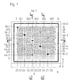
- FIGS. 1 to 6 show schematic representations of a LCD display element with five rows and five columns to explain the principle of the present invention.
- Realistic LCD display elements have more columns and rows.
- Typical LCD display elements comprise between 80 and 350 rows and columns.
- Fig. 1 shows a rectangular LCD display element with a first, optically transparent cover 1 and a second optically transparent cover 2.
- the two cover plates 1 and 2 are the same width and the first cover is slightly longer, resulting in a contact edge 4.
- the edges of the two cover plates 1 and 2 define a left side edge 5, a right side edge 6, an upper side edge 7 and a lower side edge 8.
- a layer of liquid crystal 10 is arranged - see FIGS. 4 to 6 , By an adhesive edge 12, the two optically transparent cover plates. 1 and 2 spaced apart.
- the liquid crystal 10 is completely enclosed by the two cover disks 1 and 2 and the adhesive edge 12.
- a matrix-shaped electrode arrangement 14 which, by way of example, has five substantially strip-shaped row electrodes ZE1 to ZE5 and five, substantially strip-shaped, rectangular column electrodes SE1 to SE5.
- the column electrodes SE are arranged in a first plane 16 on the inside of the first cover plate 1 and have a first electrode end 18 and a second electrode end 19.
- spacer regions 20 are provided which electrically insulate the column electrodes SE1 to SE5 from each other.
- the row electrodes ZE1 to ZE5 are arranged in a second plane 22 on the inside of the second cover 2.
- the individual row electrodes ZE1 to ZE5 are electrically isolated from one another by separation regions 24.
- the crossover areas between row and column electrodes ZE and SE define with the liquid crystal 10 therebetween the individual pixels 26 of the LCD display element.
- the area of these pixels 26 defines a rectangular viewing area 28 - in Fig. 1 shown in dashed lines, in which information can be visually displayed.
- an LCD orientation layer 30 is disposed above the row or column electrodes ZE, SE.
- Both the row inlets Z1 to Z5 and the column inlets S1 to S5 are arranged in the first plane 16 on the inside of the first cover plate 1.
- the column leads Si contact the column electrodes SEi each at their first electrode end 18.
- the column leads Si are guided in the region of the lower side edge 8 under the adhesive edge 12 to the contact edge 4.
- the row feeders Z1 to Z4 are routed between the column electrodes SE in the space regions 20.
- the fifth line feed Z5 to the fifth line electrode ZE5 is guided in the region between the first column electrode SE1 and the adhesive edge 12. Alternatively, the fifth line feed Z5 may also be arranged below the adhesive edge 12.
- Both row and column electrodes ZE, SE and row and column leads S, Z are made of ITO.
- the individual, strip-shaped row electrodes ZEi each have a constriction 32, in which the adjacent row electrodes hineinerumblen 34 with finger-like pin.
- How out Fig. 2 can be seen, extend the individual line feeders Z1 to Z5 in the first level 16 on the Entire field of view 28.
- electrical contact elements 36-i are provided which displace the liquid crystal 10 from the first plane 16 to the second plane 22 and in the region of the first plane 16 a first contact surface 46 and in the region of second level 22 have a second contact surface 40.
- the first contact surface 46 establishes the electrical contact with the respective row supply line Zi and the second contact surface 40 establishes the electrical contact with the constriction 32 of the respective row electrode ZEi.
- the spacing regions 20 are widened in the region of the electrical contact elements 36, in which the column electrodes SE have semicircular recesses 42. In this way, remains around the first contact surfaces 46 of the contact elements 36 around a sufficient isolation distance. This safely prevents short circuits.
- the electrical contact elements 36 are electrically conductive only in the direction perpendicular to the cover plates 1, 2, but not in the transverse direction thereto. This is in Fig. 4 and Fig. 6 indicated by vertical lines 44. How this electrical conductivity is achieved in only one direction, will be described below with reference to FIGS. 7d to 7e oe Congresst.
- the first line feed Z1 for driving the first row electrode ZE1 between the fourth and the fifth column electrode SE4, SE5 is arranged.
- the second line feed Z2 for driving the second line electrode ZE3 is arranged in the region between the third and the fourth column electrode SE3, SE4.
- the third line feed Z3 for driving the third line electrode ZE3 is arranged in the region between the second and the third column electrode SE2, SE3.
- the fourth line feed Z4 for driving the fourth line electrode ZE4 is arranged in the region between the first and second column electrodes SE1, SE2.
- the fifth line feed Z5 for driving the fifth line electrode ZE5 runs to the right of the first column electrode SE1.
- adhesive elements 46 and 46-i are arranged in the crossover regions of spacer regions 20 and separation regions.
- the adhesive elements 46 displace the liquid crystal 10 and connect the two cover plates 1 and 2 with each other.
- the adhesive elements 46 extend in a straight line to the left and to the right and parallel to the line spanned by the contact elements 36. Thus, between 1% and 5% of the crossover areas of separation areas 24 and spacing areas 20 are provided with adhesive elements 46.
- the symmetrically arranged to the contact elements 36 adhesive elements 46 ensures that Even with temperature changes, the electrical contact surfaces 38, 40 of the contact elements 36 with the respective line feed Zi and the constriction 32 of the respective row electrode ZEi remain in contact and no detachment takes place.
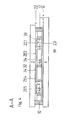
- Fig. 4 shows a sectional view through the center of the distance region 20 between the second and third column electrode SE2, SE3 along the line A - A in Fig. 1
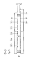
- Fig. 5 shows a sectional view along the center of the fourth column electrode SE4 and the associated fourth column lead S4 along the line B - B
- Fig. 6 shows a sectional view along the center of the third row electrode ZE3 along the line C - C in Fig. 1 ,
- FIGS. 7 and 8th FIG. 5 exemplarily shows true-to-scale embodiments of four immediately adjacent pixels 26-A, 26-B, 26-C and 26-D and 26-a, 26-b, 26c and 26-d, respectively.
- the pixels 26 have a rectangular basic shape.
- the separation regions 24 are approximately 0.05 mm wide and thus much thinner than the approximately 0.3 mm wide spacing regions 20 in which the line feed lines Z are guided.
- the width of the line feed lines Z is about 0.1 mm.
- the strip-shaped constrictions 32 of the row electrodes have a width of about 1 mm.
- the diameter of the adhesive elements 46 and the electrical contact elements 36 is about 0.3 mm.
- the individual pixels 26 have a width of 1.8 mm and a height of about 2.1 mm.
- FIGS. 7a to 7f show by way of example the electrical contact element 36-4 Fig. 1 , which connects the second row line Z2 to the second row electrode ZE2, in detail.
- Fig. 7a shows the position of the electrical contact element 36-4 in plan view of the first plane 16 with the second and third column electrodes SE2, SE3.
- Fig. 7b shows the position of the electrical contact element 36-4 in plan view of the second plane 22 with the third and second row electrode ZE3, ZE2.
- Fig. 7c shows a superposition of the FIGS. 7a and 7b.
- Fig. 7d shows the electrical contact element 36-4 Fig. 7c in magnification.
- Fig. 7e shows a section along the line A - A in Fig. 7d.
- Fig. 7f finally, it shows an enlarged section of the section Fig. 7e ,
- the electrical contact elements 36 are electrically conductive only in the direction perpendicular to the electrode assembly 14. This is achieved by a specific arrangement and configuration of electrically conductive particles 48 in the electrical contact elements 36.
- the distance d - see Fig. 7f - The insides of the two cover plates 1, 2 is about 5 up to 10 ⁇ m.
- the diameter of an electrical contact element 36 is in supervision about 0.3 mm - see Fig. 7d .
- the conductive particles 48, z. B. in the form of gold-coated plastic beads, have a mean diameter d x , which is slightly larger than the cell gap d (distance of the two cover discs 1,2). Ie.
- the mean diameter d x of the conductive particles 48 is between 10% and 20% greater than the distance d of the two cover disks 1, 2. Therefore, the conductive particles 48 between the two cover plates 1, 2 are clamped and compressed see Fig. 7f , so that the two electrical contact surfaces 38 and 40 result, which make the electrical contact with the row electrode ZE and the line feed Z. How out Fig. 7d can be seen, the single layer of electrically conductive particles 48 is statistically distributed over the cross-sectional area of the electrical contact elements 36 that results in a mean distance D between the individual particles 48, which is substantially greater than their diameter d x .
- the electrical contact elements 36 are electrically conductive in the direction perpendicular to the cover plates 1 and 2 and electrically non-conductive in the direction parallel to the two cover plates 1 and 2.
- 8a, 8b, 8c and 8d show in an analogous manner to the representation in the FIGS. 7a to 7d
- the adhesive member 46-3 between four pixels 26-a, 26b, 26-d and 26-c - see Fig. 1
- Fig. 8a shows the position of the adhesive member 46-3 in plan view of the first plane 16 with the fourth and fifth column electrodes SE4, SE5.
- Fig. 8b shows the position of the adhesive element 46-3 in plan view of the second plane 22 with the third and fourth row electrodes ZE3, ZE4.
- Fig. 8c shows a superposition of the Figures 8a and 8.
- Figure 8d shows adhesive element 46-3 Fig. 8c in magnification.
- the row electrode ZE in question and the associated column electrode SE For driving (ON state) or for non-control (OFF state) of a particular pixel P, the row electrode ZE in question and the associated column electrode SE with a sequence of row and column voltage pulses in the form of two successive square-wave voltage pulses U Z11 and U Z12 or U Z01 and U Z02 and U S11 and U S12 or U S01 and U S02 acted upon.
- the pixel P turns to the ON state when the resultant pixel voltage Up as the difference of the applied row and column voltage pulses is above the threshold voltage U threshold at which the liquid crystal 10 changes from the OFF state to the ON state.
- the threshold voltage U threshold at ⁇ 35 Vogt
- the pixel 26-A in Fig. 1 to the ON state and the pixel 26-C is turned to the OFF state the line voltage pulse train U Z11 and U Z12 , ie, 0 and 40 volts for the ON state, is applied to the row electrode Z3.
- Fig. 10 in an analogous way to Fig. 9 shown row and column voltage pulse trains, the unwanted switching to the intermediate state is easily prevented by the voltage pulse trains which are applied to row electrodes and column electrodes, are reversed. Ie.
- the row electrodes ZE are driven by the column voltage pulse trains and the column electrodes SE are driven by line voltage pulse trains according to the prior art.
- Fig. 10 shown.
- the threshold voltage U threshold of ⁇ 35 volts is clearly exceeded only for the resulting pixel voltage pulse sequence U P ⁇ 1 , U P ⁇ 2 , and the pixel in question clearly in the ON state.
- U P ⁇ 1, U P ⁇ 2, U P ⁇ 1, U P ⁇ 2 and U P ⁇ 1 U P ⁇ 2 threshold voltage U threshold of ⁇ 35 volts is significantly undershot, so that these pixel voltage pulse sequences representing all the OFF state of the respective pixel.
- U P ⁇ 2 threshold voltage U threshold of ⁇ 35 volts is significantly undershot, so that these pixel voltage pulse sequences representing all the OFF state of the respective pixel.
- For the control of individual pixels 26 results thus no difference to the state of the art. Ie. a certain pixel 26 is surely put in the ON or OFF state.
- the updating or description direction follows in the prior art Fig. 9 line by line, where all or selected lines can be described.
- the update or description direction is column by column due to the interchange of row and column voltages. Again, all or selected columns can be described.
- Individual LCD display elements according to the present invention can be connected to display panels in the same way as described with reference to FIGS. 9a, 9b and 10 in EP 1 962 129 A1 is described.
- By the shingled arrangement according to Fig. 10 in EP 1 962 129 A1 can be provided almost arbitrarily large scoreboards.
Landscapes
- Physics & Mathematics (AREA)
- Nonlinear Science (AREA)
- Mathematical Physics (AREA)
- Chemical & Material Sciences (AREA)
- Crystallography & Structural Chemistry (AREA)
- General Physics & Mathematics (AREA)
- Optics & Photonics (AREA)
- Liquid Crystal (AREA)
- Devices For Indicating Variable Information By Combining Individual Elements (AREA)
Applications Claiming Priority (1)
| Application Number | Priority Date | Filing Date | Title |
|---|---|---|---|
| DE102009032273A DE102009032273A1 (de) | 2009-07-08 | 2009-07-08 | LCD-Anzeigeelement und LCD-Anzeigetafel |
Publications (2)
| Publication Number | Publication Date |
|---|---|
| EP2284603A1 true EP2284603A1 (fr) | 2011-02-16 |
| EP2284603B1 EP2284603B1 (fr) | 2017-05-17 |
Family
ID=42542792
Family Applications (1)
| Application Number | Title | Priority Date | Filing Date |
|---|---|---|---|
| EP10168901.6A Not-in-force EP2284603B1 (fr) | 2009-07-08 | 2010-07-08 | Élément d'affichage à cristaux liquides |
Country Status (4)
| Country | Link |
|---|---|
| US (1) | US8587570B2 (fr) |
| EP (1) | EP2284603B1 (fr) |
| CA (1) | CA2709179A1 (fr) |
| DE (1) | DE102009032273A1 (fr) |
Families Citing this family (5)
| Publication number | Priority date | Publication date | Assignee | Title |
|---|---|---|---|---|
| TWI449013B (zh) * | 2012-05-22 | 2014-08-11 | Au Optronics Corp | 顯示裝置及其操作方法 |
| KR101642589B1 (ko) * | 2013-09-30 | 2016-07-29 | 주식회사 엘지화학 | 유기전자소자용 기판 및 이의 제조방법 |
| US9785032B2 (en) | 2013-11-12 | 2017-10-10 | E Ink Holdings Inc. | Active device array substrate and display panel |
| TWI505010B (zh) * | 2013-11-12 | 2015-10-21 | E Ink Holdings Inc | 主動元件陣列基板 |
| KR102422576B1 (ko) | 2015-10-14 | 2022-07-21 | 삼성디스플레이 주식회사 | 액정 표시장치 |
Citations (4)
| Publication number | Priority date | Publication date | Assignee | Title |
|---|---|---|---|---|
| JP2001311955A (ja) * | 2000-02-24 | 2001-11-09 | Seiko Epson Corp | 液晶装置及びこれを用いた電子機器 |
| US20070139299A1 (en) | 2003-07-02 | 2007-06-21 | Kent Display Incorporated | Stacked display with shared electrode addressing |
| EP1962129A1 (fr) | 2007-02-26 | 2008-08-27 | AEG Gesellschaft für moderne Informationssysteme mbH | Elément d'affichage à cristal liquide et à matrice passive, et tableau d'affichage à cristal liquide comportent plusieurs de tels éléments |
| US20080291187A1 (en) | 2006-03-30 | 2008-11-27 | Fujitsu Limited | Drive method and display device of display element |
Family Cites Families (10)
| Publication number | Priority date | Publication date | Assignee | Title |
|---|---|---|---|---|
| DE2058104C2 (de) | 1970-11-26 | 1987-01-02 | Licentia Patent-Verwaltungs-Gmbh, 6000 Frankfurt | Anzeigeelement mit einem Flüssigkristall |
| JPH0545667A (ja) | 1991-08-20 | 1993-02-26 | Hitachi Ltd | ドツトマトリクス型表示装置 |
| DE4310112A1 (de) | 1993-03-27 | 1994-09-29 | Licentia Gmbh | Flüssigkristall-Anzeigevorrichtung |
| JP3595153B2 (ja) * | 1998-03-03 | 2004-12-02 | 株式会社 日立ディスプレイズ | 液晶表示装置および映像信号線駆動手段 |
| JP3708770B2 (ja) | 1999-12-24 | 2005-10-19 | セイコーエプソン株式会社 | 液晶装置の製造方法 |
| DE50108044D1 (de) | 2000-02-24 | 2005-12-22 | Aeg Ges Moderne Inf Sys Mbh | LCD-Pixelmatrixelement und grafikfähige LCD-Anzeigetafel mit einer Mehrzahl von solchen LCD-Pixelmatrixelementen |
| JP2002244578A (ja) | 2001-02-15 | 2002-08-30 | Sanyo Electric Co Ltd | 表示装置 |
| JP3702859B2 (ja) | 2001-04-16 | 2005-10-05 | セイコーエプソン株式会社 | 電気光学装置及び電子機器 |
| US6806938B2 (en) | 2001-08-30 | 2004-10-19 | Kyocera Corporation | Liquid crystal display device with particular on substrate wiring, portable terminal and display equipment provided with the liquid crystal display device |
| KR101620048B1 (ko) * | 2010-01-20 | 2016-05-13 | 삼성디스플레이 주식회사 | 액정표시장치 및 이의 구동 방법 |
-
2009
- 2009-07-08 DE DE102009032273A patent/DE102009032273A1/de not_active Withdrawn
-
2010
- 2010-07-07 US US12/803,855 patent/US8587570B2/en not_active Expired - Fee Related
- 2010-07-07 CA CA2709179A patent/CA2709179A1/fr not_active Abandoned
- 2010-07-08 EP EP10168901.6A patent/EP2284603B1/fr not_active Not-in-force
Patent Citations (4)
| Publication number | Priority date | Publication date | Assignee | Title |
|---|---|---|---|---|
| JP2001311955A (ja) * | 2000-02-24 | 2001-11-09 | Seiko Epson Corp | 液晶装置及びこれを用いた電子機器 |
| US20070139299A1 (en) | 2003-07-02 | 2007-06-21 | Kent Display Incorporated | Stacked display with shared electrode addressing |
| US20080291187A1 (en) | 2006-03-30 | 2008-11-27 | Fujitsu Limited | Drive method and display device of display element |
| EP1962129A1 (fr) | 2007-02-26 | 2008-08-27 | AEG Gesellschaft für moderne Informationssysteme mbH | Elément d'affichage à cristal liquide et à matrice passive, et tableau d'affichage à cristal liquide comportent plusieurs de tels éléments |
Non-Patent Citations (2)
| Title |
|---|
| KANEKO E: "DIRECTLY ADDRESSED MATRIX LIQUID CRYSTAL DISPLAY PANEL WITH HIGH INFORMATION CONTENT", MOLECULAR CRYSTALS AND LIQUID CRYSTALS, GORDON AND BREACH, LONDON, GB, vol. 139, no. 1/02, 1 January 1986 (1986-01-01), pages 81 - 101, XP001079395, ISSN: 0026-8941 * |
| YANG, DENG-KE; WU, SHIN-TSON: "Fundamentals of liquid crystal devices", 2006, JOHN WILEY & SONS LTD, Chichester, West Sussex, UK, ISBN: 9780470015421, pages: 274 - 278, XP002598148 * |
Also Published As
| Publication number | Publication date |
|---|---|
| CA2709179A1 (fr) | 2011-01-08 |
| US8587570B2 (en) | 2013-11-19 |
| US20110007045A1 (en) | 2011-01-13 |
| DE102009032273A1 (de) | 2011-01-13 |
| EP2284603B1 (fr) | 2017-05-17 |
Similar Documents
| Publication | Publication Date | Title |
|---|---|---|
| DE69220071T4 (de) | Elektrophoretische anzeigevorrichtung mit verschachtelter lokaler anode | |
| DE3016364C2 (de) | Flüssigkristall-Anzeigevorrichtung mit matrixartiger Anordnung der Erregerelektroden | |
| DE19841760B4 (de) | Flüssigkristallanzeigevorrichtung mit einem verbesserten leitenden Bereich | |
| DE10117874B4 (de) | Flüssigkristallanzeige | |
| DE3223986C2 (fr) | ||
| DE10139095B4 (de) | Flüssigkristallanzeige | |
| DE69635647T2 (de) | Flüssigkristallanzeigevorrichtung | |
| DE3035268A1 (de) | Fluessigkristall-anzeigematrix | |
| DE3855793T2 (de) | Schaltungen mit mehreren Ebenen, Verfahren zum Herstellen derselben und Anzeigevorrichtung mit solchen Schaltungen | |
| DE69332935T2 (de) | Flache Anzeigevorrichtung, ihr Ansteuerungsverfahren und Verfahren zu ihrer Herstellung | |
| EP2284603B1 (fr) | Élément d'affichage à cristaux liquides | |
| DE69830435T2 (de) | Räumlischer LichtModulator und Anzeige | |
| DE102004031108B4 (de) | In der Ebene schaltendes Flüssigkristalldisplay und Arraysubstrat für ein solches | |
| DE2848508A1 (de) | Elektrodenanordnung an einer fluessigkristall-anzeigeeinrichtung | |
| DE3402469C2 (de) | Flüssigkristallanzeigevorrichtung | |
| DE69018618T2 (de) | Aktive flüssigkristall-punktmatrix-anzeigestruktur mit hoher auflösung. | |
| DE69533187T2 (de) | Elektrooptische Anzeigevorrichtung | |
| EP1962129B1 (fr) | Elément d'affichage à cristal liquide et à matrice passive, et tableau d'affichage à cristal liquide comportent plusieurs de tels éléments | |
| DE69430895T2 (de) | Anzeigevorrichtung mit Flüssigkristallen | |
| DE2302698A1 (de) | Fluessigkristallanzeigevorrichtung | |
| DE69127588T2 (de) | Optisches Modulationselement und sein Herstellungsverfahren | |
| DE2660634C1 (de) | Fluessigkristall-Matrixanzeige | |
| DE68922473T2 (de) | Wiedergabeanordnung. | |
| DE2542189B2 (de) | Fluessigkristallanzeige mit bistabiler cholesterinischer fluessigkristall- schicht | |
| DE102010021456A1 (de) | Panel |
Legal Events
| Date | Code | Title | Description |
|---|---|---|---|
| PUAI | Public reference made under article 153(3) epc to a published international application that has entered the european phase |
Free format text: ORIGINAL CODE: 0009012 |
|
| AK | Designated contracting states |
Kind code of ref document: A1 Designated state(s): AL AT BE BG CH CY CZ DE DK EE ES FI FR GB GR HR HU IE IS IT LI LT LU LV MC MK MT NL NO PL PT RO SE SI SK SM TR |
|
| AX | Request for extension of the european patent |
Extension state: BA ME RS |
|
| 17P | Request for examination filed |
Effective date: 20110810 |
|
| 17Q | First examination report despatched |
Effective date: 20140710 |
|
| RAP1 | Party data changed (applicant data changed or rights of an application transferred) |
Owner name: BMG GESELLSCHAFT FUER MODERNE INFORMATIONSSYSTEME |
|
| GRAP | Despatch of communication of intention to grant a patent |
Free format text: ORIGINAL CODE: EPIDOSNIGR1 |
|
| RIC1 | Information provided on ipc code assigned before grant |
Ipc: G02F 1/1345 20060101AFI20161020BHEP Ipc: G02F 1/1343 20060101ALI20161020BHEP Ipc: G09G 3/36 20060101ALI20161020BHEP |
|
| INTG | Intention to grant announced |
Effective date: 20161124 |
|
| GRAS | Grant fee paid |
Free format text: ORIGINAL CODE: EPIDOSNIGR3 |
|
| GRAA | (expected) grant |
Free format text: ORIGINAL CODE: 0009210 |
|
| AK | Designated contracting states |
Kind code of ref document: B1 Designated state(s): AL AT BE BG CH CY CZ DE DK EE ES FI FR GB GR HR HU IE IS IT LI LT LU LV MC MK MT NL NO PL PT RO SE SI SK SM TR |
|
| REG | Reference to a national code |
Ref country code: GB Ref legal event code: FG4D Free format text: NOT ENGLISH |
|
| REG | Reference to a national code |
Ref country code: CH Ref legal event code: EP |
|
| REG | Reference to a national code |
Ref country code: IE Ref legal event code: FG4D Free format text: LANGUAGE OF EP DOCUMENT: GERMAN |
|
| REG | Reference to a national code |
Ref country code: AT Ref legal event code: REF Ref document number: 894991 Country of ref document: AT Kind code of ref document: T Effective date: 20170615 |
|
| REG | Reference to a national code |
Ref country code: DE Ref legal event code: R096 Ref document number: 502010013606 Country of ref document: DE |
|
| REG | Reference to a national code |
Ref country code: NL Ref legal event code: MP Effective date: 20170517 |
|
| REG | Reference to a national code |
Ref country code: LT Ref legal event code: MG4D |
|
| PG25 | Lapsed in a contracting state [announced via postgrant information from national office to epo] |
Ref country code: GR Free format text: LAPSE BECAUSE OF FAILURE TO SUBMIT A TRANSLATION OF THE DESCRIPTION OR TO PAY THE FEE WITHIN THE PRESCRIBED TIME-LIMIT Effective date: 20170818 Ref country code: ES Free format text: LAPSE BECAUSE OF FAILURE TO SUBMIT A TRANSLATION OF THE DESCRIPTION OR TO PAY THE FEE WITHIN THE PRESCRIBED TIME-LIMIT Effective date: 20170517 Ref country code: FI Free format text: LAPSE BECAUSE OF FAILURE TO SUBMIT A TRANSLATION OF THE DESCRIPTION OR TO PAY THE FEE WITHIN THE PRESCRIBED TIME-LIMIT Effective date: 20170517 Ref country code: HR Free format text: LAPSE BECAUSE OF FAILURE TO SUBMIT A TRANSLATION OF THE DESCRIPTION OR TO PAY THE FEE WITHIN THE PRESCRIBED TIME-LIMIT Effective date: 20170517 Ref country code: LT Free format text: LAPSE BECAUSE OF FAILURE TO SUBMIT A TRANSLATION OF THE DESCRIPTION OR TO PAY THE FEE WITHIN THE PRESCRIBED TIME-LIMIT Effective date: 20170517 Ref country code: NO Free format text: LAPSE BECAUSE OF FAILURE TO SUBMIT A TRANSLATION OF THE DESCRIPTION OR TO PAY THE FEE WITHIN THE PRESCRIBED TIME-LIMIT Effective date: 20170817 |
|
| PG25 | Lapsed in a contracting state [announced via postgrant information from national office to epo] |
Ref country code: NL Free format text: LAPSE BECAUSE OF FAILURE TO SUBMIT A TRANSLATION OF THE DESCRIPTION OR TO PAY THE FEE WITHIN THE PRESCRIBED TIME-LIMIT Effective date: 20170517 Ref country code: BG Free format text: LAPSE BECAUSE OF FAILURE TO SUBMIT A TRANSLATION OF THE DESCRIPTION OR TO PAY THE FEE WITHIN THE PRESCRIBED TIME-LIMIT Effective date: 20170817 Ref country code: LV Free format text: LAPSE BECAUSE OF FAILURE TO SUBMIT A TRANSLATION OF THE DESCRIPTION OR TO PAY THE FEE WITHIN THE PRESCRIBED TIME-LIMIT Effective date: 20170517 Ref country code: IS Free format text: LAPSE BECAUSE OF FAILURE TO SUBMIT A TRANSLATION OF THE DESCRIPTION OR TO PAY THE FEE WITHIN THE PRESCRIBED TIME-LIMIT Effective date: 20170917 Ref country code: PL Free format text: LAPSE BECAUSE OF FAILURE TO SUBMIT A TRANSLATION OF THE DESCRIPTION OR TO PAY THE FEE WITHIN THE PRESCRIBED TIME-LIMIT Effective date: 20170517 Ref country code: SE Free format text: LAPSE BECAUSE OF FAILURE TO SUBMIT A TRANSLATION OF THE DESCRIPTION OR TO PAY THE FEE WITHIN THE PRESCRIBED TIME-LIMIT Effective date: 20170517 |
|
| PG25 | Lapsed in a contracting state [announced via postgrant information from national office to epo] |
Ref country code: SK Free format text: LAPSE BECAUSE OF FAILURE TO SUBMIT A TRANSLATION OF THE DESCRIPTION OR TO PAY THE FEE WITHIN THE PRESCRIBED TIME-LIMIT Effective date: 20170517 Ref country code: DK Free format text: LAPSE BECAUSE OF FAILURE TO SUBMIT A TRANSLATION OF THE DESCRIPTION OR TO PAY THE FEE WITHIN THE PRESCRIBED TIME-LIMIT Effective date: 20170517 Ref country code: RO Free format text: LAPSE BECAUSE OF FAILURE TO SUBMIT A TRANSLATION OF THE DESCRIPTION OR TO PAY THE FEE WITHIN THE PRESCRIBED TIME-LIMIT Effective date: 20170517 Ref country code: EE Free format text: LAPSE BECAUSE OF FAILURE TO SUBMIT A TRANSLATION OF THE DESCRIPTION OR TO PAY THE FEE WITHIN THE PRESCRIBED TIME-LIMIT Effective date: 20170517 Ref country code: CZ Free format text: LAPSE BECAUSE OF FAILURE TO SUBMIT A TRANSLATION OF THE DESCRIPTION OR TO PAY THE FEE WITHIN THE PRESCRIBED TIME-LIMIT Effective date: 20170517 |
|
| REG | Reference to a national code |
Ref country code: DE Ref legal event code: R097 Ref document number: 502010013606 Country of ref document: DE |
|
| PG25 | Lapsed in a contracting state [announced via postgrant information from national office to epo] |
Ref country code: IT Free format text: LAPSE BECAUSE OF FAILURE TO SUBMIT A TRANSLATION OF THE DESCRIPTION OR TO PAY THE FEE WITHIN THE PRESCRIBED TIME-LIMIT Effective date: 20170517 Ref country code: SM Free format text: LAPSE BECAUSE OF FAILURE TO SUBMIT A TRANSLATION OF THE DESCRIPTION OR TO PAY THE FEE WITHIN THE PRESCRIBED TIME-LIMIT Effective date: 20170517 |
|
| PLBE | No opposition filed within time limit |
Free format text: ORIGINAL CODE: 0009261 |
|
| STAA | Information on the status of an ep patent application or granted ep patent |
Free format text: STATUS: NO OPPOSITION FILED WITHIN TIME LIMIT |
|
| REG | Reference to a national code |
Ref country code: IE Ref legal event code: MM4A |
|
| 26N | No opposition filed |
Effective date: 20180220 |
|
| GBPC | Gb: european patent ceased through non-payment of renewal fee |
Effective date: 20170817 |
|
| REG | Reference to a national code |
Ref country code: FR Ref legal event code: ST Effective date: 20180330 |
|
| PG25 | Lapsed in a contracting state [announced via postgrant information from national office to epo] |
Ref country code: IE Free format text: LAPSE BECAUSE OF NON-PAYMENT OF DUE FEES Effective date: 20170708 |
|
| PG25 | Lapsed in a contracting state [announced via postgrant information from national office to epo] |
Ref country code: SI Free format text: LAPSE BECAUSE OF FAILURE TO SUBMIT A TRANSLATION OF THE DESCRIPTION OR TO PAY THE FEE WITHIN THE PRESCRIBED TIME-LIMIT Effective date: 20170517 Ref country code: FR Free format text: LAPSE BECAUSE OF NON-PAYMENT OF DUE FEES Effective date: 20170731 |
|
| REG | Reference to a national code |
Ref country code: BE Ref legal event code: MM Effective date: 20170731 |
|
| PG25 | Lapsed in a contracting state [announced via postgrant information from national office to epo] |
Ref country code: LU Free format text: LAPSE BECAUSE OF NON-PAYMENT OF DUE FEES Effective date: 20170708 |
|
| PG25 | Lapsed in a contracting state [announced via postgrant information from national office to epo] |
Ref country code: GB Free format text: LAPSE BECAUSE OF NON-PAYMENT OF DUE FEES Effective date: 20170817 |
|
| PG25 | Lapsed in a contracting state [announced via postgrant information from national office to epo] |
Ref country code: BE Free format text: LAPSE BECAUSE OF NON-PAYMENT OF DUE FEES Effective date: 20170731 |
|
| PG25 | Lapsed in a contracting state [announced via postgrant information from national office to epo] |
Ref country code: MT Free format text: LAPSE BECAUSE OF FAILURE TO SUBMIT A TRANSLATION OF THE DESCRIPTION OR TO PAY THE FEE WITHIN THE PRESCRIBED TIME-LIMIT Effective date: 20170517 |
|
| PGFP | Annual fee paid to national office [announced via postgrant information from national office to epo] |
Ref country code: DE Payment date: 20180619 Year of fee payment: 9 |
|
| PGFP | Annual fee paid to national office [announced via postgrant information from national office to epo] |
Ref country code: CH Payment date: 20180725 Year of fee payment: 9 Ref country code: AT Payment date: 20180719 Year of fee payment: 9 |
|
| PG25 | Lapsed in a contracting state [announced via postgrant information from national office to epo] |
Ref country code: MC Free format text: LAPSE BECAUSE OF FAILURE TO SUBMIT A TRANSLATION OF THE DESCRIPTION OR TO PAY THE FEE WITHIN THE PRESCRIBED TIME-LIMIT Effective date: 20170517 Ref country code: HU Free format text: LAPSE BECAUSE OF FAILURE TO SUBMIT A TRANSLATION OF THE DESCRIPTION OR TO PAY THE FEE WITHIN THE PRESCRIBED TIME-LIMIT; INVALID AB INITIO Effective date: 20100708 |
|
| PG25 | Lapsed in a contracting state [announced via postgrant information from national office to epo] |
Ref country code: CY Free format text: LAPSE BECAUSE OF NON-PAYMENT OF DUE FEES Effective date: 20170517 |
|
| PG25 | Lapsed in a contracting state [announced via postgrant information from national office to epo] |
Ref country code: MK Free format text: LAPSE BECAUSE OF FAILURE TO SUBMIT A TRANSLATION OF THE DESCRIPTION OR TO PAY THE FEE WITHIN THE PRESCRIBED TIME-LIMIT Effective date: 20170517 |
|
| REG | Reference to a national code |
Ref country code: DE Ref legal event code: R119 Ref document number: 502010013606 Country of ref document: DE |
|
| REG | Reference to a national code |
Ref country code: CH Ref legal event code: PL |
|
| REG | Reference to a national code |
Ref country code: AT Ref legal event code: MM01 Ref document number: 894991 Country of ref document: AT Kind code of ref document: T Effective date: 20190708 |
|
| PG25 | Lapsed in a contracting state [announced via postgrant information from national office to epo] |
Ref country code: TR Free format text: LAPSE BECAUSE OF FAILURE TO SUBMIT A TRANSLATION OF THE DESCRIPTION OR TO PAY THE FEE WITHIN THE PRESCRIBED TIME-LIMIT Effective date: 20170517 |
|
| PG25 | Lapsed in a contracting state [announced via postgrant information from national office to epo] |
Ref country code: DE Free format text: LAPSE BECAUSE OF NON-PAYMENT OF DUE FEES Effective date: 20200201 Ref country code: AT Free format text: LAPSE BECAUSE OF NON-PAYMENT OF DUE FEES Effective date: 20190708 |
|
| PG25 | Lapsed in a contracting state [announced via postgrant information from national office to epo] |
Ref country code: PT Free format text: LAPSE BECAUSE OF FAILURE TO SUBMIT A TRANSLATION OF THE DESCRIPTION OR TO PAY THE FEE WITHIN THE PRESCRIBED TIME-LIMIT Effective date: 20170517 Ref country code: CH Free format text: LAPSE BECAUSE OF NON-PAYMENT OF DUE FEES Effective date: 20190731 Ref country code: LI Free format text: LAPSE BECAUSE OF NON-PAYMENT OF DUE FEES Effective date: 20190731 |
|
| PG25 | Lapsed in a contracting state [announced via postgrant information from national office to epo] |
Ref country code: AL Free format text: LAPSE BECAUSE OF FAILURE TO SUBMIT A TRANSLATION OF THE DESCRIPTION OR TO PAY THE FEE WITHIN THE PRESCRIBED TIME-LIMIT Effective date: 20170517 |