EP2284860A2 - Résistance électrique et commutateur d'installation doté d'une résistance électrique - Google Patents
Résistance électrique et commutateur d'installation doté d'une résistance électrique Download PDFInfo
- Publication number
- EP2284860A2 EP2284860A2 EP10008110A EP10008110A EP2284860A2 EP 2284860 A2 EP2284860 A2 EP 2284860A2 EP 10008110 A EP10008110 A EP 10008110A EP 10008110 A EP10008110 A EP 10008110A EP 2284860 A2 EP2284860 A2 EP 2284860A2
- Authority
- EP
- European Patent Office
- Prior art keywords
- pieces
- sheet metal
- resistance element
- resistor
- stacking direction
- Prior art date
- Legal status (The legal status is an assumption and is not a legal conclusion. Google has not performed a legal analysis and makes no representation as to the accuracy of the status listed.)
- Withdrawn
Links
Images

Classifications
-
- H—ELECTRICITY
- H01—ELECTRIC ELEMENTS
- H01H—ELECTRIC SWITCHES; RELAYS; SELECTORS; EMERGENCY PROTECTIVE DEVICES
- H01H71/00—Details of the protective switches or relays covered by groups H01H73/00 - H01H83/00
- H01H71/10—Operating or release mechanisms
- H01H71/1081—Modifications for selective or back-up protection; Correlation between feeder and branch circuit breaker
-
- H—ELECTRICITY
- H01—ELECTRIC ELEMENTS
- H01C—RESISTORS
- H01C3/00—Non-adjustable metal resistors made of wire or ribbon, e.g. coiled, woven or formed as grids
- H01C3/06—Flexible or folding resistors, whereby such a resistor can be looped or collapsed upon itself
-
- H—ELECTRICITY
- H01—ELECTRIC ELEMENTS
- H01C—RESISTORS
- H01C3/00—Non-adjustable metal resistors made of wire or ribbon, e.g. coiled, woven or formed as grids
- H01C3/10—Non-adjustable metal resistors made of wire or ribbon, e.g. coiled, woven or formed as grids the resistive element having zig-zag or sinusoidal configuration
-
- H—ELECTRICITY
- H01—ELECTRIC ELEMENTS
- H01H—ELECTRIC SWITCHES; RELAYS; SELECTORS; EMERGENCY PROTECTIVE DEVICES
- H01H71/00—Details of the protective switches or relays covered by groups H01H73/00 - H01H83/00
- H01H71/10—Operating or release mechanisms
- H01H71/12—Automatic release mechanisms with or without manual release
- H01H71/40—Combined electrothermal and electromagnetic mechanisms
Definitions
- the invention relates to an electrical resistor, in particular a selective resistor for a selective main circuit breaker, with a resistance element and at least two connecting pieces associated with the resistance element, according to the preamble of claim 1.
- the invention also relates to a method for producing an electrical resistance according to claim 11.
- the invention also relates to an electrical switching device having a first contact point, which is moved in a short circuit of an electromagnetic actuator in the open position, and with a second contact point, which is permanently opened by a first thermal release via a switch lock, and with a parallel to arranged in the first contact point parallel current path, in which a current-limiting resistor is arranged, according to the preamble of claim 12th
- Known generic resistors that can be designed as high load resistance due to their purpose, for example, designed as a wound wire wound resistors.
- Such wound wire wound resistors can be very voluminous in design on short-circuit load and thus require a relatively large installation space in a service switching device. claim.
- large-scale wirewound resistors have a relatively high weight.
- insufficient heat dissipation takes place in the known wound wire resistors via the connecting wires, so that heat build-up can occur in the region of the resistance element itself, whereby overheating is accelerated in the event of a short-circuit load.
- an installation switching device is shown with a resistor, wherein the resistor is made there as a resistance wire, for example made of CrAl1255, Cu or other alloys, wherein the wire is wound into a coil, due to their design and the required resistance value, a relatively large amount of space claimed.
- a coil-shaped resistor generates a large magnetic field, so that the coil must be wound consuming antiparallel.
- the coil When using bare wires, the coil must be wound on a high-temperature-resistant support body, to prevent the windings attract when energized and thus cause a Windungsschluß. If the resistance wire is insulated, then come as insulating expensive and poorly manageable materials such. B. glass silk used.
- the present invention is therefore in the light of the prior art, the object of developing a generic electrical resistance to the effect that he has a high resistance to short-circuit load, a space-saving form with low weight and large heat dissipation to the electrical connections and cost while a simple structure can be produced, and to provide a method for producing such a resistor.
- the invention has the object, an improved electrical service switching device with a first contact point, which is moved in the event of a short circuit of an electromagnetic actuator in the open position, and with a second contact point of a first thermal release via a switching mechanism is permanently opened, and with a parallel to the first contact point arranged parallel current path, in which a current-limiting resistor is arranged to create, which has a high resistance to short-circuit load in a small design and easy to assemble at large heat dissipation from the resistor and is inexpensive to produce.
- the resistance element is formed from a stack of partial sheet metal pieces consisting of a resistance sheet material, wherein the partial sheet metal pieces are arranged with their broad sides parallel to each other and in the stacking direction one behind the other and spaced from each other, wherein adjacent part sheet metal pieces in the stacking direction alternately right and left a perpendicular to the broad side of the partial sheet metal pieces extending center plane are electrically connected to each other at their narrow sides, so that the current path from the first, edge sheet metal piece to the opposite stacking, second edge sheet metal piece meandering through the remaining part sheet metal pieces.
- the first and the second marginal sheet metal piece form the electrical connection pieces.
- the partial sheet metal pieces are held by means of at least one holding device made of insulating material at a distance from each other.
- finger-like incisions are formed in the partial sheet metal pieces, which alternately extend in each case from a first edge side in the direction of the respective opposite edge side, so that the current path in a partial piece of sheet metal between the two narrow sides takes a meandering course ,
- the resistance element consists of a metal strip which is folded transversely to the strip direction.
- the folds extending laterally in the longitudinal direction of the band connect directly to each other with adjacent partial band pieces.
- the folds are formed substantially zig-zag-shaped, and the resistance element is compressed in a holding device arranged such that the zig-zag course of the folds in favor of substantially parallel to each other in the stacking direction successively arranged part-band pieces is overcome.
- the resistance element is folded meander-shaped.
- a gap is left between adjacent part-tape pieces in the stacking direction.
- the resistance element is a stamped and bent part, wherein the finger-like cuts of the partial sheet metal pieces are punched out in the metal strip.
- the object underlying the invention is achieved with respect to the service switching device by a generic service switching device in which the current-limiting resistor comprises a resistor element and at least two connecting elements associated with the resistor element, and wherein the resistor element is formed from a stack of partial sheet metal pieces, which consists of a resistance sheet material exist, wherein the partial sheet metal pieces with their broad sides parallel to each other and in the stacking direction one behind the other and from each other are arranged, wherein adjacent part-sheet metal pieces in the stacking direction alternately right and left of a perpendicular to the broad side of the partial sheet metal pieces extending center plane are electrically connected to each other at their narrow sides, so that the current path from the first, marginal piece of sheet metal to the stacking direction, second marginal piece of sheet metal meandering through the remaining part sheet metal pieces.
- An advantageous embodiment of a service switching device is characterized in that the resistance element consists of a metal strip which is folded transversely to the belt direction, and that the folds extending laterally in the belt longitudinal direction connect directly adjacent partial belt pieces with each other.
- a further advantageous embodiment of an installation switching device is characterized in that the folds are formed substantially zigzag-shaped, and that the resistance element is arranged in such a compressed manner in a holding device, that the zigzag-shaped course of the folds in favor of substantially parallel is overcome in the stacking direction successively arranged part-tape pieces.
- a further advantageous embodiment of a service switching device is characterized in that at least one conductor section, with which the resistor is switched into the parallel current path, resiliently presses against the first or the second marginal piece of sheet metal.
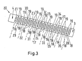
- FIG. 3 shows a metal strip 20 made of a resistance metal, for example, from CrAl1255, Cu or other alloys.
- the metal strip 20 is elongated and has two edge sides 16, 17 running parallel in the direction of longitudinal extension.
- Several finger-like incisions 19, 18 are formed in the metal strip 20, which are arranged one behind the other in the longitudinal direction of the metal strip 20 so as to form an interdigital structure.
- the cuts 18, 19 can be punched particularly favorable from the metal strip 20.
- the folding web 21 is adjoined by a narrow finger-like incision which, starting from the upper edge side 16, extends in the direction of the lower edge side 17, again without reaching it.
- the finger-like incisions run parallel to each other and perpendicular to the longitudinal direction of the edge sides 16, 17.
- At the outgoing of the upper edge 16 incision joins outgoing from the lower edge 17 side incision, then again emanating from the upper edge 16 side and back on from the lower edge side 17 outgoing, and then a broad finger-like incision, which extends from the upper edge side 16 in the direction of the lower edge side 17.
- a folding web 22 similar to the folding web 21 as described above.
- the two folding webs 21 and 22 define between them a partial tape piece 29 in which an interdigital structure is stamped.
- the described sequence of narrow and wide cuts continues to the right in the longitudinal direction of the metal strip 20.
- the partial band piece 29 is adjoined by a partial band piece 30 which lies between the folding web 22 and a further folding web 23 which is again located on the upper edge side 16.
- Further partial band pieces 31, 32, 33, 34, 35 are each bounded by folding webs 24, 25, 26, 27, 28 lying alternately on the upper and lower edge sides 16, 17.
- the last folding web 28 is adjoined by a second connecting piece 3 in which there are two narrow cuts and thus form an interdigital structure in the connecting piece 3 only on its first half.
- the right part of the second connecting piece 3 is without incision and forms a smooth connection surface.
- a current path extending from the first connection piece 4 to the second connection piece 3 is forced into a looped or meandering path because of the interdigital structure formed by the cuts 18, 19, so that the flow path lengthens with reduced cross-sectional area and thus the flow path electrical resistance of the metal strip increases.
- the resistance value of the electrical resistance of the metal strip 20 can thus be adjusted to a desired value.
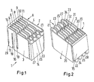
- FIG. 1 shows a resistor 1 with the resistance element 2 in isometric view on the side of the second connector 3 whereas FIG. 2 shows the resistance in isometric view on the side of the first connector 4.
- the partial band pieces 4, 29, 30, 31, 32, 33, 34, 35, 3 are in the manner of a sheet stack in parallel and spaced from one another in the stacking direction A. Therefore, the partial band pieces are also generally referred to as partial sheet metal pieces 5, 6, 7, 8, 9, 10, 11. On their narrow sides, they are alternately connected electrically by the folds or folding webs 21, 22, 23, 24, 25, 26, 27, 28.
- the current path from the first terminal 4 to the second terminal 3 now runs to a certain extent in a double meander, once in the meander on the metal strip 20, as described above, and second in the meandering fold, the stack according to FIGS. 1 and 2 forms.
- the partial sheet metal pieces 4, 5, 6, 7, 8, 9, 10, 11, 3 held by a holding device 14, 15 of insulating material at a distance.
- This is here a holding plate from the rib-like retaining walls protrude vertically.
- the retaining walls fix the partial sheet metal pieces and prevent them from being compressed so far that they could touch each other and thus create a short circuit between adjacent partial sheet metal pieces. Therefore, a separate insulation, such as an insulating layer on the metal strip 20, can be dispensed with. This has the advantage that a higher thermal load capacity of the resistor 1 is given. In fact, an insulating layer would have a lower temperature resistance than the metal strip 20.
- the holding device can be made of an insulating material with high heat resistance, such as ceramic or a heavy-duty plastic.
- a coating of the metal strip 20 with such a heavy-duty plastic would be too expensive.
- Another advantage is the small footprint, which thus arises for a heavy-duty resistance element.
- the metal strip 20 can be inexpensively manufactured as a stamped and bent part.
- the marginal part band pieces 3, 4 are well suited as large-scale fittings.
- the resistor 1 can be particularly advantageous clamped with contact clamping springs on the two part-tape pieces 3, 4 and thus electrically and mechanically installed at its destination. A good heat dissipation can be achieved via the large-area connection pieces 3, 4, which is advantageous for highly loaded resistors.
- a resistor according to the invention could also be obtained in a different way than described above by folding a metal strip. It would be possible, for example, to bring partial sheet metal pieces 3, 5, 6, 7, 8, 9, 10, 11, 4 in stacking direction A one behind the other into a holding device 14, 15 and then connect them electrically alternately on their narrow sides on the right and left, for example by one soldered or welded corresponding connectors, or by attaching wire bridges or sheet metal bridges.
- the above-described manner of producing a resistance according to the invention by folding a sheet-metal strip is a very elegant and economical procedure, but the invention should not be limited thereto.
- a selective main circuit breaker 40 as shown in the Fig. 4 is shown schematically, has a housing 42 which may be formed either of a cup-shaped housing lower part and a lid or two approximately the same shell halves. Within this housing 42 is a first contact point 41 with a fixed contact piece 44 and a movable contact piece 43.
- the movable contact piece 43 which is arranged on a pivotable contact lever 45, is pivoted by an electromagnet when a short-circuit current occurs, so that the contact point 41st is opened.
- This contact point 41 is associated with a parallel current path 46, in which a resistor 1 is located. When the contact point 41 is opened, there arises an arc which migrates into an arc splitter stack 47.
- the main circuit breaker 40 can also be switched by hand. For this purpose, he has a handle 53 which cooperates with a rear derailleur 52.
- the rear derailleur 52 also provides for a permanent open position of the contact point 41. Details of the structure of the rear derailleur and the rest of the internal structure of a main line circuit breaker are known and, for example in the DE 102008016035 A1 to which reference is made in this regard.
- the contacting of the resistor 1 by means of ribbon conductors 48 and 49 The conductor 48 may be formed as a straight component, and the conductor 49 may have in the region of the contacting surface 3, 4 of the resistor 1 has a convex portion to the contacting surface. Instead of a rectilinear conductor 48, it is also possible to use one which has a section convex toward the contacting surface 3, 4 of the resistor 1. At least one of the two conductor pieces 48, 49 is resilient. Both conductor pieces 48, 49 can also be resilient.
- the conductor 49 may be formed so that it with an angled portion 50 and a bend or angle 51, the resistor. 1 holds.
- the resistor 1 by a contact spring (not shown here) resiliently contacted and held it.
- the internal structure of the service switching device 40 is in Fig. 4 only very schematically and exemplified, with many details that are not related to the design or storage of the resistor 1, are not shown.
- Other known installation switching devices, with different circuit diagram and other spatial arrangement of the inner assemblies are therefore covered by the present invention, as long as they include only one resistor 1 as described in the present invention.
Landscapes
- Engineering & Computer Science (AREA)
- Microelectronics & Electronic Packaging (AREA)
- Push-Button Switches (AREA)
- Apparatuses And Processes For Manufacturing Resistors (AREA)
- Details Of Resistors (AREA)
- Arc-Extinguishing Devices That Are Switches (AREA)
Applications Claiming Priority (1)
| Application Number | Priority Date | Filing Date | Title |
|---|---|---|---|
| DE102009036227.4A DE102009036227B4 (de) | 2009-08-05 | 2009-08-05 | Elektrischer Widerstand, Verfahren zu seiner Herstellung und Installationsschaltgerät mit elektrischem Widerstand |
Publications (2)
| Publication Number | Publication Date |
|---|---|
| EP2284860A2 true EP2284860A2 (fr) | 2011-02-16 |
| EP2284860A3 EP2284860A3 (fr) | 2012-07-25 |
Family
ID=43029253
Family Applications (1)
| Application Number | Title | Priority Date | Filing Date |
|---|---|---|---|
| EP10008110A Withdrawn EP2284860A3 (fr) | 2009-08-05 | 2010-08-04 | Résistance électrique et commutateur d'installation doté d'une résistance électrique |
Country Status (3)
| Country | Link |
|---|---|
| EP (1) | EP2284860A3 (fr) |
| CN (2) | CN101996718A (fr) |
| DE (1) | DE102009036227B4 (fr) |
Cited By (1)
| Publication number | Priority date | Publication date | Assignee | Title |
|---|---|---|---|---|
| JP2021534586A (ja) * | 2018-08-17 | 2021-12-09 | エルエス、エレクトリック、カンパニー、リミテッドLs Electric Co., Ltd. | モジュール型限流抵抗器 |
Families Citing this family (3)
| Publication number | Priority date | Publication date | Assignee | Title |
|---|---|---|---|---|
| DE102009036227B4 (de) * | 2009-08-05 | 2015-02-05 | Abb Ag | Elektrischer Widerstand, Verfahren zu seiner Herstellung und Installationsschaltgerät mit elektrischem Widerstand |
| DE102016206799A1 (de) * | 2016-04-21 | 2017-10-26 | Siemens Aktiengesellschaft | Widerstand und Kompaktleistungsschalter |
| CN110752075B (zh) * | 2019-10-12 | 2022-03-15 | 许继变压器有限公司 | 一种并联选线中电阻 |
Citations (3)
| Publication number | Priority date | Publication date | Assignee | Title |
|---|---|---|---|---|
| DE2854711A1 (de) | 1978-12-18 | 1980-07-03 | Bbc Brown Boveri & Cie | Selektivschutzeinrichtung |
| DE10203443A1 (de) | 2002-01-30 | 2003-07-31 | Abb Patent Gmbh | Elektrisches Schaltgerät |
| DE102008016035A1 (de) | 2008-03-28 | 2009-10-01 | Abb Ag | Installationsschaltgerät |
Family Cites Families (8)
| Publication number | Priority date | Publication date | Assignee | Title |
|---|---|---|---|---|
| DE950867C (de) * | 1939-12-06 | 1956-10-18 | Sachsenwerk Licht & Kraft Ag | Aus Blechstreifen bestehender Widerstandskoerper |
| CH250845A (de) * | 1942-06-02 | 1947-09-30 | Satchwell Leonard | Verfahren zur Herstellung eines induktionsfreien, gitterförmigen, elektrischen Widerstandselementes. |
| GB557794A (en) * | 1942-06-02 | 1943-12-06 | Leonard Satchwell | Improvements in or relating to electric resistance grids |
| DE1800293U (de) * | 1958-09-17 | 1959-11-19 | Bbc Brown Boveri & Cie | Gefalteter widerstand. |
| DE4008422A1 (de) * | 1990-03-16 | 1991-09-19 | Asea Brown Boveri | Leistungswiderstand |
| US5917404A (en) * | 1997-01-13 | 1999-06-29 | Ipc Resistors, Inc. | Power resistor |
| DE102004033680B4 (de) * | 2004-07-09 | 2009-03-12 | Wobben, Aloys, Dipl.-Ing. | Lastwiderstand |
| DE102009036227B4 (de) * | 2009-08-05 | 2015-02-05 | Abb Ag | Elektrischer Widerstand, Verfahren zu seiner Herstellung und Installationsschaltgerät mit elektrischem Widerstand |
-
2009
- 2009-08-05 DE DE102009036227.4A patent/DE102009036227B4/de not_active Expired - Fee Related
-
2010
- 2010-08-04 EP EP10008110A patent/EP2284860A3/fr not_active Withdrawn
- 2010-08-05 CN CN2010102550262A patent/CN101996718A/zh active Pending
- 2010-08-05 CN CN2010202953926U patent/CN201966013U/zh not_active Expired - Fee Related
Patent Citations (3)
| Publication number | Priority date | Publication date | Assignee | Title |
|---|---|---|---|---|
| DE2854711A1 (de) | 1978-12-18 | 1980-07-03 | Bbc Brown Boveri & Cie | Selektivschutzeinrichtung |
| DE10203443A1 (de) | 2002-01-30 | 2003-07-31 | Abb Patent Gmbh | Elektrisches Schaltgerät |
| DE102008016035A1 (de) | 2008-03-28 | 2009-10-01 | Abb Ag | Installationsschaltgerät |
Cited By (2)
| Publication number | Priority date | Publication date | Assignee | Title |
|---|---|---|---|---|
| JP2021534586A (ja) * | 2018-08-17 | 2021-12-09 | エルエス、エレクトリック、カンパニー、リミテッドLs Electric Co., Ltd. | モジュール型限流抵抗器 |
| US11355268B2 (en) | 2018-08-17 | 2022-06-07 | Ls Electric Co., Ltd. | Modular current limiting resistor |
Also Published As
| Publication number | Publication date |
|---|---|
| DE102009036227A1 (de) | 2011-02-17 |
| DE102009036227B4 (de) | 2015-02-05 |
| CN201966013U (zh) | 2011-09-07 |
| EP2284860A3 (fr) | 2012-07-25 |
| CN101996718A (zh) | 2011-03-30 |
Similar Documents
| Publication | Publication Date | Title |
|---|---|---|
| EP2732507B1 (fr) | Connecteur enfichable à courant fort pour applications dans des véhicules à moteur | |
| DE102010017872B4 (de) | Bistabiles Kleinrelais großer Leistung | |
| EP3595090B1 (fr) | Borne de connexion conductrice | |
| DE69930845T2 (de) | Gehäuse für schmelzsicherungsschalter | |
| DE102017109210B4 (de) | Relais | |
| DE4323426C2 (de) | Klemmkontaktvorrichtung | |
| EP1470565B1 (fr) | Appareil de distribution electrique | |
| EP2284860A2 (fr) | Résistance électrique et commutateur d'installation doté d'une résistance électrique | |
| DE2838214A1 (de) | Piezoelektrische schaltvorrichtung | |
| DE3111901C2 (fr) | ||
| DE102011089251B4 (de) | Auslöseeinheit zum Betätigen einer mechanischen Schalteinheit einer Vorrichtung | |
| EP0798750A2 (fr) | Résistance de limitation de courant à comportement PTC | |
| DE4009428A1 (de) | Elektromagnetisches schaltschuetz | |
| EP2197010B1 (fr) | Agencement de sécurité de commutateur pour systèmes de barres de raccordement | |
| DE102012005031A1 (de) | Installationsschaltgerät | |
| DE102014106957A1 (de) | Relais | |
| DE2513494C2 (de) | Temperaturschutzschalter für Rohrheizkörper | |
| DE3225830C2 (de) | Elektromagnetisches Drehankerrelais | |
| DE19700758C1 (de) | Schalter mit mindestens einem feststehenden Schaltstück | |
| DE102006007603A1 (de) | Relais mit reduziertem Kriechstrom | |
| DE112016001407T5 (de) | Spulenanschluss und damit versehenes elektromagnetisches Relais | |
| DE3331847A1 (de) | Kabeltrommel | |
| DE202017006764U1 (de) | Relais | |
| DE102008016035A1 (de) | Installationsschaltgerät | |
| DE1184015B (de) | Verfahren zur Herstellung von Eisenkreisteilen fuer gekapselte magnetisch steuerbare Kontaktvorrichtungen |
Legal Events
| Date | Code | Title | Description |
|---|---|---|---|
| PUAI | Public reference made under article 153(3) epc to a published international application that has entered the european phase |
Free format text: ORIGINAL CODE: 0009012 |
|
| AK | Designated contracting states |
Kind code of ref document: A2 Designated state(s): AL AT BE BG CH CY CZ DE DK EE ES FI FR GB GR HR HU IE IS IT LI LT LU LV MC MK MT NL NO PL PT RO SE SI SK SM TR |
|
| AX | Request for extension of the european patent |
Extension state: BA ME RS |
|
| PUAL | Search report despatched |
Free format text: ORIGINAL CODE: 0009013 |
|
| AK | Designated contracting states |
Kind code of ref document: A3 Designated state(s): AL AT BE BG CH CY CZ DE DK EE ES FI FR GB GR HR HU IE IS IT LI LT LU LV MC MK MT NL NO PL PT RO SE SI SK SM TR |
|
| AX | Request for extension of the european patent |
Extension state: BA ME RS |
|
| RIC1 | Information provided on ipc code assigned before grant |
Ipc: H01H 71/10 20060101AFI20120619BHEP Ipc: H01H 71/40 20060101ALN20120619BHEP Ipc: H01C 3/10 20060101ALI20120619BHEP Ipc: H01C 3/06 20060101ALI20120619BHEP |
|
| 17P | Request for examination filed |
Effective date: 20130112 |
|
| STAA | Information on the status of an ep patent application or granted ep patent |
Free format text: STATUS: THE APPLICATION IS DEEMED TO BE WITHDRAWN |
|
| 18D | Application deemed to be withdrawn |
Effective date: 20160301 |