EP2284862A1 - Système et procédé pour la sélection et le positionnement de matrices de puces - Google Patents
Système et procédé pour la sélection et le positionnement de matrices de puces Download PDFInfo
- Publication number
- EP2284862A1 EP2284862A1 EP09167653A EP09167653A EP2284862A1 EP 2284862 A1 EP2284862 A1 EP 2284862A1 EP 09167653 A EP09167653 A EP 09167653A EP 09167653 A EP09167653 A EP 09167653A EP 2284862 A1 EP2284862 A1 EP 2284862A1
- Authority
- EP
- European Patent Office
- Prior art keywords
- chip die
- chip
- pickup head
- die
- active side
- Prior art date
- Legal status (The legal status is an assumption and is not a legal conclusion. Google has not performed a legal analysis and makes no representation as to the accuracy of the status listed.)
- Withdrawn
Links
Images
Classifications
-
- H—ELECTRICITY
- H10—SEMICONDUCTOR DEVICES; ELECTRIC SOLID-STATE DEVICES NOT OTHERWISE PROVIDED FOR
- H10W—GENERIC PACKAGES, INTERCONNECTIONS, CONNECTORS OR OTHER CONSTRUCTIONAL DETAILS OF DEVICES COVERED BY CLASS H10
- H10W95/00—Packaging processes not covered by the other groups of this subclass
-
- H—ELECTRICITY
- H10—SEMICONDUCTOR DEVICES; ELECTRIC SOLID-STATE DEVICES NOT OTHERWISE PROVIDED FOR
- H10P—GENERIC PROCESSES OR APPARATUS FOR THE MANUFACTURE OR TREATMENT OF DEVICES COVERED BY CLASS H10
- H10P72/00—Handling or holding of wafers, substrates or devices during manufacture or treatment thereof
- H10P72/70—Handling or holding of wafers, substrates or devices during manufacture or treatment thereof for supporting or gripping
- H10P72/78—Handling or holding of wafers, substrates or devices during manufacture or treatment thereof for supporting or gripping using vacuum or suction, e.g. Bernoulli chucks
-
- G—PHYSICS
- G01—MEASURING; TESTING
- G01R—MEASURING ELECTRIC VARIABLES; MEASURING MAGNETIC VARIABLES
- G01R31/00—Arrangements for testing electric properties; Arrangements for locating electric faults; Arrangements for electrical testing characterised by what is being tested not provided for elsewhere
- G01R31/28—Testing of electronic circuits, e.g. by signal tracer
- G01R31/2851—Testing of integrated circuits [IC]
- G01R31/2893—Handling, conveying or loading, e.g. belts, boats, vacuum fingers
-
- H—ELECTRICITY
- H05—ELECTRIC TECHNIQUES NOT OTHERWISE PROVIDED FOR
- H05K—PRINTED CIRCUITS; CASINGS OR CONSTRUCTIONAL DETAILS OF ELECTRIC APPARATUS; MANUFACTURE OF ASSEMBLAGES OF ELECTRICAL COMPONENTS
- H05K13/00—Apparatus or processes specially adapted for manufacturing or adjusting assemblages of electric components
- H05K13/04—Mounting of components, e.g. of leadless components
-
- H—ELECTRICITY
- H10—SEMICONDUCTOR DEVICES; ELECTRIC SOLID-STATE DEVICES NOT OTHERWISE PROVIDED FOR
- H10P—GENERIC PROCESSES OR APPARATUS FOR THE MANUFACTURE OR TREATMENT OF DEVICES COVERED BY CLASS H10
- H10P72/00—Handling or holding of wafers, substrates or devices during manufacture or treatment thereof
- H10P72/04—Apparatus for manufacture or treatment
- H10P72/0446—Apparatus for mounting on conductive members, e.g. leadframes or conductors on insulating substrates
-
- H—ELECTRICITY
- H10—SEMICONDUCTOR DEVICES; ELECTRIC SOLID-STATE DEVICES NOT OTHERWISE PROVIDED FOR
- H10P—GENERIC PROCESSES OR APPARATUS FOR THE MANUFACTURE OR TREATMENT OF DEVICES COVERED BY CLASS H10
- H10P95/00—Generic processes or apparatus for manufacture or treatments not covered by the other groups of this subclass
Definitions
- the invention relates to the field of picking and placing of a chip die in a chip manufacturing process.
- a chip die manipulator apparatus arranged for picking and placing of a chip die in a chip manufacturing process, comprising: first and second pickup heads arranged to pick up a chip die with an active side facing the first pickup head; and pick the chip die from the first pickup head, to have the active side facing away from the second pickup head; and an aligner system for aligning the second pickup head relative to a substrate to place the chip die, wherein the first pickup head comprises a test card comprising contact pads arranged to contact the active side of the chip die; and a clamp for clamping the chip die against the contact pads.
- a method of picking and placing of a chip die in a chip manufacturing process comprising: providing first and second a pickup heads, the first pickup head comprising a test card with contact pads arranged to contact the chip die's active side; and a clamp for clamping the chip die against the contact pads; clamping the chip die's active side to the test card's contact pads to have the active side facing the first pickup head; and providing a chip die test by the test card; performing, consecutively, a flip chip movement of the chip die, to have the active side facing away from the second pickup head or have the chip die rejected; and aligning the second pickup head relative to a substrate to place the chip die.
- Advantages may include reduction of the number of process steps and providing less breakdown risk in the manufacturing process due to in-place testing of chip dies.
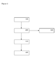
- FIG. 1 there is provided a schematic of typical production steps 100-400 for a chip-flip manufacturing process according to an aspect of the invention.
- the method relies on providing first and second a pickup heads as further exemplified in Figure 2 , the first pickup head comprising a test card with contact pads arranged to contact the chip die's active side; and a clamp for clamping the chip die against the contact pads.
- the need for in place reliability testing will increase.
- a chip die's active side is clamped to a test card's contact pads to have the active side facing a first pickup head.
- an electrical chip die test is performed by the test card.
- Typical tests can be found in the art, for example in the cited US5796264 , which is incorporated herein by reference.
- a wafer probe includes various functional and parametric tests of each die. Test patterns, timing voltage margins, limits and test sequence are determined by individual product yields and reliability data.
- Four testing levels (C1, C2, C3, C7) have been established for semiconductor die.
- Standard probe (C1) level includes the standard test for gross functionality.
- Speed probe (C2) level tests the speed performance of a die for the fastest speed grades.
- Burned-in die (C3) level includes a burn-in test.
- Known good die (C7) level involves testing to provide a quality and reliability equal to package products. Any of these tests and/or variations or additions to these can be performed in principle.
- a flip chip movement of the chip die is performed, to have the active side facing away from the second pickup head.
- the chip die is rejected in alternative step 320 and the process sequence is aborted.
- the second pickup head is aligned in a fourth step 400 relative to a substrate to place the chip die prior to placing the chip die on the substrate.
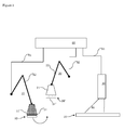
- FIG 2 schematically shows an example of a chip die manipulator apparatus 10 according to an aspect of the invention, executing the steps discussed with reference to Figure 1 . It is assumed that die 30 are presented with the contact side 31 up (as usual after dicing). The first step gathers the die from on diced wafer via manipulator 10.
- the manipulator apparatus comprises a pickup head 11 arranged to pick up the chip die 30 with an active side 31 facing the first pickup head 11 and a second pickup head 21 arranged to perform a flip chip movement of the chip die 30. It is noted that the flipping can be performed by either the first or second pickup head 11, 21. The result is shown in Figure 2 as greyed chip die 30', having the active side 31' facing away from the second pickup head 21.
- the second manipulator 20 holds the die 30' with the active side 31' exposed, so the die 30 can be placed and bonded to the receiving body 50 (e.g. a substrate or other die).
- First and second pickup heads 11 and 21 are actuated by manipulator arms 12 and 22 to form first and second manipulators 10 and 20.
- the manipulator apparatus is provided with a control system 60 controlling the actuating movement of manipulators 10 and 20 via signal lines 61 and 62 respectively, further, and alignment system 40 is provided to align the pickup head 21 via signal line 63, for proper placement of the chip die 30 to substrate 50. Placement can be done by optical inspection 41 or any other alignment method known in the art.
- any clamping method to clamp the die 30 to the pickup head 11 may be feasible, for example, spring clamping, electrostatic clamping or any other clamping method, preferably the clamping is performed by vacuum clamping as further exemplified in Figure 3 .
- the die to be placed is held with the contact side 31 against pickup head 11 of manipulator 10, wherein a chip die test is performed.
- the first pickup head 11 comprises a test card (see further example Figure 3 ) comprising contact pads arranged to contact the active side of the chip die; and a clamp for clamping the chip die against the contact pads.
- the die can be tested for electrical performance during the total time the die resides within the flip-manipulator.
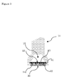
- Figure 3 shows a further example of such a test card arrangement 12.
- the test card 12 comprises vacuum via channels 13 arranged over substantially an entire contact surface to clamp the die over its entire surface for coupling with a vacuum pressure source (not shown), so as to provide a clamping force to the chip die 30 by vacuum clamping.
- the test card 12 can be mounted in a vacuum pressure orifice 15 of pickup head 11, preferably held by detachable couplings. This can be adjusted for specific die layouts of active surfaces 31, so that any bonding contacts 32 of chip die 30 are brought in contact with corresponding pads or bumps 14 of the test card.
- test card 12 is kept relative to the vacuum pressure orifice 15 to couple the vacuum pressure via the vacuum via channels 13 to the chip die 30, which is accordingly held clamped against the test card 12.
- the test card may be made of suitable materials such as silicon, glass or epoxy based substrate material.
- the vacuum will hold the die under test and secure proper contact of the bumps 32 on the die 30 with the contacts 14 on the test card 12.
- the vacuum pressure ensures good contact against the contact pads 14.
- an additional advantage of this invention is that the complete die 30 is supported during the flip-action including release from the carrier. In particular for thin die this is beneficial in comparison with present contact type pick-up nozzles that may damage the die 30 during pick-up from the carrier wafer.
- the electrical test can be carried out. Finally the die is released from the vacuum and transferred to the second manipulator fro placement.
- the invention can be applied during all movements in pick-and-place equipment, provided that the die to be tested is held at the contact side.
- test card structure can be equipped with additional circuitry such as a multiplexer die, or such multiplexe function could be integrated directly in the test structure in case of a silicon test structure.
- the invention may provide the following merits:
- this technique enables the potential for timely repairing a stack with a defective chip since testing can be done conveniently during flip chip bonding.
- test used herein is not limited to a specified physical designs, but may encompass all kinds of structures that may interconnect with chip die.
- the invention is not limited to specific types of tests but may include all kind of device and integrity tests, including electrical, optical and mechanical integrity.
Landscapes
- Engineering & Computer Science (AREA)
- Microelectronics & Electronic Packaging (AREA)
- Computer Hardware Design (AREA)
- General Engineering & Computer Science (AREA)
- Physics & Mathematics (AREA)
- General Physics & Mathematics (AREA)
- Manufacturing & Machinery (AREA)
- Testing Or Measuring Of Semiconductors Or The Like (AREA)
Priority Applications (5)
| Application Number | Priority Date | Filing Date | Title |
|---|---|---|---|
| EP09167653A EP2284862A1 (fr) | 2009-08-11 | 2009-08-11 | Système et procédé pour la sélection et le positionnement de matrices de puces |
| KR1020127006159A KR20120059543A (ko) | 2009-08-11 | 2010-08-10 | 칩 다이들의 선발 및 위치화를 위한 시스템 및 방법 |
| PCT/NL2010/050502 WO2011019275A1 (fr) | 2009-08-11 | 2010-08-10 | Système et procédé pour saisir et placer des matrices à puce |
| EP10760113A EP2465135A1 (fr) | 2009-08-11 | 2010-08-10 | Système et procédé pour saisir et placer des matrices à puce |
| US13/390,134 US20120194209A1 (en) | 2009-08-11 | 2010-08-10 | System and method for picking and placement of chip dies |
Applications Claiming Priority (1)
| Application Number | Priority Date | Filing Date | Title |
|---|---|---|---|
| EP09167653A EP2284862A1 (fr) | 2009-08-11 | 2009-08-11 | Système et procédé pour la sélection et le positionnement de matrices de puces |
Publications (1)
| Publication Number | Publication Date |
|---|---|
| EP2284862A1 true EP2284862A1 (fr) | 2011-02-16 |
Family
ID=41395763
Family Applications (2)
| Application Number | Title | Priority Date | Filing Date |
|---|---|---|---|
| EP09167653A Withdrawn EP2284862A1 (fr) | 2009-08-11 | 2009-08-11 | Système et procédé pour la sélection et le positionnement de matrices de puces |
| EP10760113A Withdrawn EP2465135A1 (fr) | 2009-08-11 | 2010-08-10 | Système et procédé pour saisir et placer des matrices à puce |
Family Applications After (1)
| Application Number | Title | Priority Date | Filing Date |
|---|---|---|---|
| EP10760113A Withdrawn EP2465135A1 (fr) | 2009-08-11 | 2010-08-10 | Système et procédé pour saisir et placer des matrices à puce |
Country Status (4)
| Country | Link |
|---|---|
| US (1) | US20120194209A1 (fr) |
| EP (2) | EP2284862A1 (fr) |
| KR (1) | KR20120059543A (fr) |
| WO (1) | WO2011019275A1 (fr) |
Cited By (2)
| Publication number | Priority date | Publication date | Assignee | Title |
|---|---|---|---|---|
| TWI452310B (zh) * | 2012-05-03 | 2014-09-11 | Chroma Ate Inc | Test device for stacked wafers |
| EP3509094A1 (fr) * | 2018-01-09 | 2019-07-10 | Acer Incorporated | Equipement de transfert de micro dispositifs et méthode associée |
Families Citing this family (1)
| Publication number | Priority date | Publication date | Assignee | Title |
|---|---|---|---|---|
| GB2511087A (en) | 2013-02-22 | 2014-08-27 | Ibm | System for electrical testing and manufacturing a 3D chip stack and method |
Citations (7)
| Publication number | Priority date | Publication date | Assignee | Title |
|---|---|---|---|---|
| EP0162207A1 (fr) * | 1984-03-28 | 1985-11-27 | International Business Machines Corporation | Méthode et appareil pour tester des dispositifs électriques |
| EP0257546A2 (fr) * | 1986-08-21 | 1988-03-02 | Matsushita Electric Industrial Co., Ltd. | Machine de placement de puces à fonction de contrôle |
| US5796264A (en) | 1991-06-04 | 1998-08-18 | Micron Technology, Inc. | Apparatus for manufacturing known good semiconductor dice |
| US6171049B1 (en) * | 1996-02-29 | 2001-01-09 | Alphasem Ag | Method and device for receiving, orientating and assembling of components |
| WO2001067831A2 (fr) * | 2000-03-10 | 2001-09-13 | Infotech Ag | Systeme a camera unique servant a l'alignement d'un composant sur un substrat |
| US20020036411A1 (en) * | 1999-10-27 | 2002-03-28 | Quick Keith W. | Apparatus and method for handling an integrated circuit |
| WO2006118018A1 (fr) * | 2005-04-28 | 2006-11-09 | Toray Engineering Co., Ltd. | Procede d’inspection du deplacement d’une connexion par billes et appareil de montage |
Family Cites Families (4)
| Publication number | Priority date | Publication date | Assignee | Title |
|---|---|---|---|---|
| US5905382A (en) * | 1990-08-29 | 1999-05-18 | Micron Technology, Inc. | Universal wafer carrier for wafer level die burn-in |
| IT1272853B (it) * | 1994-11-30 | 1997-06-30 | Circuit Line Spa | Metodo e apparecchiatura per il carico e lo scarico automatico di circuiti stampati su macchine per l'esecuzione del test elettrico |
| US5966903A (en) * | 1998-05-27 | 1999-10-19 | Lucent Technologies Inc. | High speed flip-chip dispensing |
| TWI287634B (en) * | 2004-12-31 | 2007-10-01 | Wen-Chang Dung | Micro-electromechanical probe circuit film, method for making the same and applications thereof |
-
2009
- 2009-08-11 EP EP09167653A patent/EP2284862A1/fr not_active Withdrawn
-
2010
- 2010-08-10 EP EP10760113A patent/EP2465135A1/fr not_active Withdrawn
- 2010-08-10 WO PCT/NL2010/050502 patent/WO2011019275A1/fr not_active Ceased
- 2010-08-10 KR KR1020127006159A patent/KR20120059543A/ko not_active Withdrawn
- 2010-08-10 US US13/390,134 patent/US20120194209A1/en not_active Abandoned
Patent Citations (7)
| Publication number | Priority date | Publication date | Assignee | Title |
|---|---|---|---|---|
| EP0162207A1 (fr) * | 1984-03-28 | 1985-11-27 | International Business Machines Corporation | Méthode et appareil pour tester des dispositifs électriques |
| EP0257546A2 (fr) * | 1986-08-21 | 1988-03-02 | Matsushita Electric Industrial Co., Ltd. | Machine de placement de puces à fonction de contrôle |
| US5796264A (en) | 1991-06-04 | 1998-08-18 | Micron Technology, Inc. | Apparatus for manufacturing known good semiconductor dice |
| US6171049B1 (en) * | 1996-02-29 | 2001-01-09 | Alphasem Ag | Method and device for receiving, orientating and assembling of components |
| US20020036411A1 (en) * | 1999-10-27 | 2002-03-28 | Quick Keith W. | Apparatus and method for handling an integrated circuit |
| WO2001067831A2 (fr) * | 2000-03-10 | 2001-09-13 | Infotech Ag | Systeme a camera unique servant a l'alignement d'un composant sur un substrat |
| WO2006118018A1 (fr) * | 2005-04-28 | 2006-11-09 | Toray Engineering Co., Ltd. | Procede d’inspection du deplacement d’une connexion par billes et appareil de montage |
Cited By (3)
| Publication number | Priority date | Publication date | Assignee | Title |
|---|---|---|---|---|
| TWI452310B (zh) * | 2012-05-03 | 2014-09-11 | Chroma Ate Inc | Test device for stacked wafers |
| EP3509094A1 (fr) * | 2018-01-09 | 2019-07-10 | Acer Incorporated | Equipement de transfert de micro dispositifs et méthode associée |
| US10505070B2 (en) | 2018-01-09 | 2019-12-10 | Acer Incorporated | Micro device transfer equipment and related method |
Also Published As
| Publication number | Publication date |
|---|---|
| EP2465135A1 (fr) | 2012-06-20 |
| WO2011019275A1 (fr) | 2011-02-17 |
| US20120194209A1 (en) | 2012-08-02 |
| KR20120059543A (ko) | 2012-06-08 |
Similar Documents
| Publication | Publication Date | Title |
|---|---|---|
| US8957691B2 (en) | Probe cards for probing integrated circuits | |
| US7541203B1 (en) | Conductive adhesive for thinned silicon wafers with through silicon vias | |
| US7750651B2 (en) | Wafer level test probe card | |
| US9207276B2 (en) | Method and apparatus for testing a semiconductor wafer | |
| CN102854343B (zh) | 用于半导体器件的测试结构和测试方法 | |
| CN101657894B (zh) | 用于单切管芯测试的方法和装置 | |
| JP5489132B2 (ja) | 薄型基板による電子素子のパッケージ方法 | |
| TW200822263A (en) | Test method for yielding a known good die | |
| CN103887193B (zh) | 用于三维集成电路测试的装置 | |
| US8884639B2 (en) | Methods, apparatus and articles of manufacture for testing a plurality of singulated die | |
| JP5489133B2 (ja) | 薄型基板による電子素子のパッケージ方法 | |
| KR101350499B1 (ko) | 시험 장치, 시험 방법 및 제조 방법 | |
| CN101821634A (zh) | 多部位探针 | |
| TW522438B (en) | Method for producing semiconductor device | |
| JP5489131B2 (ja) | 薄型基板による電子素子のパッケージ方法 | |
| EP2284862A1 (fr) | Système et procédé pour la sélection et le positionnement de matrices de puces | |
| US9581639B2 (en) | Organic space transformer attachment and assembly | |
| CN101501510A (zh) | 测试单个管芯的装置和方法 | |
| US8667669B2 (en) | Apparatus and method for manufacturing a packaged device | |
| US6881593B2 (en) | Semiconductor die adapter and method of using | |
| KR101615999B1 (ko) | 프로브 카드 제조용 웨이퍼 핀 어레이 프레임 모듈 |
Legal Events
| Date | Code | Title | Description |
|---|---|---|---|
| PUAI | Public reference made under article 153(3) epc to a published international application that has entered the european phase |
Free format text: ORIGINAL CODE: 0009012 |
|
| AK | Designated contracting states |
Kind code of ref document: A1 Designated state(s): AT BE BG CH CY CZ DE DK EE ES FI FR GB GR HR HU IE IS IT LI LT LU LV MC MK MT NL NO PL PT RO SE SI SK SM TR |
|
| AX | Request for extension of the european patent |
Extension state: AL BA RS |
|
| STAA | Information on the status of an ep patent application or granted ep patent |
Free format text: STATUS: THE APPLICATION IS DEEMED TO BE WITHDRAWN |
|
| 18D | Application deemed to be withdrawn |
Effective date: 20110817 |