EP2284867B1 - Siliciumkarbid-Halbleitervorrichtung - Google Patents
Siliciumkarbid-Halbleitervorrichtung Download PDFInfo
- Publication number
- EP2284867B1 EP2284867B1 EP10014514.3A EP10014514A EP2284867B1 EP 2284867 B1 EP2284867 B1 EP 2284867B1 EP 10014514 A EP10014514 A EP 10014514A EP 2284867 B1 EP2284867 B1 EP 2284867B1
- Authority
- EP
- European Patent Office
- Prior art keywords
- substrate
- sic
- film
- insulating film
- gate
- Prior art date
- Legal status (The legal status is an assumption and is not a legal conclusion. Google has not performed a legal analysis and makes no representation as to the accuracy of the status listed.)
- Ceased
Links
Images




Classifications
-
- H—ELECTRICITY
- H10—SEMICONDUCTOR DEVICES; ELECTRIC SOLID-STATE DEVICES NOT OTHERWISE PROVIDED FOR
- H10D—INORGANIC ELECTRIC SEMICONDUCTOR DEVICES
- H10D12/00—Bipolar devices controlled by the field effect, e.g. insulated-gate bipolar transistors [IGBT]
- H10D12/01—Manufacture or treatment
- H10D12/031—Manufacture or treatment of IGBTs
-
- H—ELECTRICITY
- H10—SEMICONDUCTOR DEVICES; ELECTRIC SOLID-STATE DEVICES NOT OTHERWISE PROVIDED FOR
- H10D—INORGANIC ELECTRIC SEMICONDUCTOR DEVICES
- H10D1/00—Resistors, capacitors or inductors
- H10D1/60—Capacitors
- H10D1/62—Capacitors having potential barriers
- H10D1/66—Conductor-insulator-semiconductor capacitors, e.g. MOS capacitors
-
- H—ELECTRICITY
- H10—SEMICONDUCTOR DEVICES; ELECTRIC SOLID-STATE DEVICES NOT OTHERWISE PROVIDED FOR
- H10D—INORGANIC ELECTRIC SEMICONDUCTOR DEVICES
- H10D12/00—Bipolar devices controlled by the field effect, e.g. insulated-gate bipolar transistors [IGBT]
- H10D12/411—Insulated-gate bipolar transistors [IGBT]
- H10D12/441—Vertical IGBTs
-
- H—ELECTRICITY
- H10—SEMICONDUCTOR DEVICES; ELECTRIC SOLID-STATE DEVICES NOT OTHERWISE PROVIDED FOR
- H10D—INORGANIC ELECTRIC SEMICONDUCTOR DEVICES
- H10D30/00—Field-effect transistors [FET]
- H10D30/60—Insulated-gate field-effect transistors [IGFET]
- H10D30/64—Double-diffused metal-oxide semiconductor [DMOS] FETs
- H10D30/66—Vertical DMOS [VDMOS] FETs
-
- H—ELECTRICITY
- H10—SEMICONDUCTOR DEVICES; ELECTRIC SOLID-STATE DEVICES NOT OTHERWISE PROVIDED FOR
- H10D—INORGANIC ELECTRIC SEMICONDUCTOR DEVICES
- H10D62/00—Semiconductor bodies, or regions thereof, of devices having potential barriers
- H10D62/80—Semiconductor bodies, or regions thereof, of devices having potential barriers characterised by the materials
- H10D62/83—Semiconductor bodies, or regions thereof, of devices having potential barriers characterised by the materials being Group IV materials, e.g. B-doped Si or undoped Ge
- H10D62/832—Semiconductor bodies, or regions thereof, of devices having potential barriers characterised by the materials being Group IV materials, e.g. B-doped Si or undoped Ge being Group IV materials comprising two or more elements, e.g. SiGe
- H10D62/8325—Silicon carbide
-
- H—ELECTRICITY
- H10—SEMICONDUCTOR DEVICES; ELECTRIC SOLID-STATE DEVICES NOT OTHERWISE PROVIDED FOR
- H10D—INORGANIC ELECTRIC SEMICONDUCTOR DEVICES
- H10D64/00—Electrodes of devices having potential barriers
- H10D64/01—Manufacture or treatment
- H10D64/011—Manufacture or treatment of electrodes ohmically coupled to a semiconductor
- H10D64/0111—Manufacture or treatment of electrodes ohmically coupled to a semiconductor to Group IV semiconductors
- H10D64/0115—Manufacture or treatment of electrodes ohmically coupled to a semiconductor to Group IV semiconductors to silicon carbide
-
- H—ELECTRICITY
- H10—SEMICONDUCTOR DEVICES; ELECTRIC SOLID-STATE DEVICES NOT OTHERWISE PROVIDED FOR
- H10D—INORGANIC ELECTRIC SEMICONDUCTOR DEVICES
- H10D64/00—Electrodes of devices having potential barriers
- H10D64/01—Manufacture or treatment
- H10D64/013—Manufacture or treatment of electrodes having a conductor capacitively coupled to a semiconductor by an insulator
- H10D64/01366—Manufacture or treatment of electrodes having a conductor capacitively coupled to a semiconductor by an insulator the semiconductor being silicon carbide
-
- H—ELECTRICITY
- H10—SEMICONDUCTOR DEVICES; ELECTRIC SOLID-STATE DEVICES NOT OTHERWISE PROVIDED FOR
- H10D—INORGANIC ELECTRIC SEMICONDUCTOR DEVICES
- H10D64/00—Electrodes of devices having potential barriers
- H10D64/20—Electrodes characterised by their shapes, relative sizes or dispositions
- H10D64/23—Electrodes carrying the current to be rectified, amplified, oscillated or switched, e.g. sources, drains, anodes or cathodes
- H10D64/251—Source or drain electrodes for field-effect devices
- H10D64/256—Source or drain electrodes for field-effect devices for lateral devices wherein the source or drain electrodes are recessed in semiconductor bodies
-
- H—ELECTRICITY
- H10—SEMICONDUCTOR DEVICES; ELECTRIC SOLID-STATE DEVICES NOT OTHERWISE PROVIDED FOR
- H10D—INORGANIC ELECTRIC SEMICONDUCTOR DEVICES
- H10D64/00—Electrodes of devices having potential barriers
- H10D64/60—Electrodes characterised by their materials
- H10D64/62—Electrodes ohmically coupled to a semiconductor
-
- H—ELECTRICITY
- H10—SEMICONDUCTOR DEVICES; ELECTRIC SOLID-STATE DEVICES NOT OTHERWISE PROVIDED FOR
- H10D—INORGANIC ELECTRIC SEMICONDUCTOR DEVICES
- H10D8/00—Diodes
- H10D8/01—Manufacture or treatment
- H10D8/051—Manufacture or treatment of Schottky diodes
Definitions
- the present invention generally relates to a silicon carbide (SiC) semiconductor device. Further described but not part of the invention is a method for manufacturing the SiC semiconductor device, and more particularly a method of manufacturing a gate oxide film of a SiC semiconductor device having a MOS (Metal-Oxide-Semiconductor) structure.
- SiC silicon carbide
- MOS Metal-Oxide-Semiconductor
- Silicon carbide devices exist that are capable of operating under high pressure and temperature with extremely low loss. This is due to the use of a large diameter wafer (presently 4H-SiC with a diameter of up to 4 inches), the use of which was previously problematic as a result of the low channel mobility of a MOS interface.
- a SiC-MOS device MOSFET or IGBT
- IGBT currently available Si-IGBTs. Thus, it is considered as one of the most preferred switching devices, which have the power region of several kV or less.
- Silicon carbide semiconductor devices are the only wide gap semiconductor device capable of generating silicon oxide by thermal oxidation, which has been an influential basis for asserting the advantages of the silicon carbide semiconductor device.
- a gate oxide film forms by thermal oxidation of silicon carbide and presents the following problems: (1) an extremely short life span against time dependent dielectric breakdown compared to a thermal oxide film of a silicon substrate; and (2) the high defect rate due to the large wafer area.
- US 2003/107041 A1 discloses a silicon carbide semiconductor device and manufacturing method therefor, a metal electrode which is another than a gate electrode and which is contacted with a singlecrystalline silicon carbide substrate is treated with a predetermined heat process at a temperature which is lower than a thermal oxidization temperature by which a gate insulating film is formed and is sufficient to carry out a contact annealing between the singlecrystalline silicon carbide substrate and a metal after a whole surrounding of the gate insulating film is enclosed with the singlecrystalline silicon carbide substrate, a field insulating film, and the gate electrode. It is applicable to a MOS capacitor, an n channel planar power MOSFET, and an n channel planar power IGBT.
- a method of manufacturing a silicon carbide (SiC) semiconductor device with a metal-oxide-semiconductor (MOS) structure including a SiC substrate, a gate oxide film formed on a surface of the SiC substrate and a gate electrode formed on the gate oxide film, the method comprising increasing a temperature to at least a predetermined temperature while maintaining the SiC substrate in an inert gas atmosphere, when the temperature rises to at least the predetermined temperature, forming the gate oxide film by thermally-oxidizing the SiC substrate by introducing an oxidation gas and when a thickness of the gate oxide film becomes a predetermined thickness, decreasing the temperature by stopping the thermal oxidation of the SiC substrate while stopping the introduction of the oxidation gas and reestablishing the inert gas atmosphere.
- SiC silicon carbide
- MOS metal-oxide-semiconductor
- the present invention is defined in the appended claims and concerns a silicon carbide (SiC) semiconductor device with a metal-oxide-semiconductor (MOS) structure, the device comprising: a SiC substrate; a gate electrode made from polycrystalline silicon (Si); a gate oxide film formed by thermally-oxidizing the SiC substrate, the gate oxide film is disposed between the SiC substrate and the gate electrode, and connected to the SiC substrate and the gate electrode, the thickness of the gate oxide film is 20 nm or less; an ohmic contact electrically connected to the SiC substrate; and a polycrystalline silicon thermally-oxidized film formed by oxidizing a surface of the gate electrode, wherein the silicon carbide (SiC) semiconductor device is obtained by: increasing a temperature to at least a predetermined temperature while maintaining the SiC substrate in an inert gas atmosphere; when the temperature rises to at least the predetermined temperature, forming the gate oxide film by thermally-oxidizing the SiC substrate by introducing an oxidation gas; when a thickness
- thermally-oxidizing the SiC substrate comprises performing dry oxidation in a dry atmosphere with the oxidation gas being oxygen, nitrous oxide, nitric oxide, nitrogen dioxide, mixtures thereof, or a gas formed by diluting oxygen, nitrous oxide, nitric oxide, nitrogen dioxide or mixtures thereof with an inert gas.
- the oxidation gas being oxygen, nitrous oxide, nitric oxide, nitrogen dioxide, mixtures thereof, or a gas formed by diluting oxygen, nitrous oxide, nitric oxide, nitrogen dioxide or mixtures thereof with an inert gas.
- thermally-oxidizing the SiC substrate is performed at a temperature of 1,000 °C to 1,280 °C.
- the method not falling under the scope of the present invention may comprise initially forming an epitaxial layer on a principal surface of the SiC substrate, wherein the gate oxide film is formed by thermally oxidizing a surface layer of the epitaxial layer.
- the predetermined thickness is about 15 nm or less.
- the predetermined thickness is between about 8 nm to about 15 nm.
- thermally oxidizing the SiC substrate forms a lower insulating film
- the method further comprising forming a field insulating film by laying an upper insulating film on the lower insulating film, the upper insulating film formed by a process other than the thermal oxidation.
- the method not falling under the scope of the present invention may comprise opening a gate window in a part of the field insulating film, exposing the gate oxide film, and forming a gate electrode by depositing polycrystalline silicon on the gate oxide film and the field insulating film.
- the method not falling under the scope of the present invention comprises initially forming an epitaxial layer on a principal surface of the SiC substrate, wherein the gate oxide film is formed by thermally oxidizing a surface layer of the epitaxial layer.
- a silicon carbide (SiC) semiconductor device with a metal-oxide-semiconductor (MOS) structure including a SiC substrate is formed.
- a gate oxide film is formed on a surface of the SiC substrate, and a gate electrode is formed on the gate oxide film.
- the method of manufacturing such a device comprises increasing a temperature to at least a predetermined temperature while maintaining the SiC substrate in an inert gas atmosphere, forming the gate oxide film by thermally-oxidizing the SiC substrate by introducing an oxidation gas when the temperature rises to at least the predetermined temperature and decreasing the temperature by stopping the thermal oxidation of the SiC substrate while stopping the introduction of the oxidation gas and reestablishing the inert gas atmosphere when a thickness of the gate oxide film becomes a predetermined thickness.
- SiC silicon carbide
- SiO 2 silicon oxide
- MOS Metal-Oxide-Semiconductor
- TDDB time dependent dielectric breakdown
- MCTB medium charge to breakdown
- Table 1 compares the MCTB and expansion of a TDDB life Q BD (C/cm 2 ) of a gate oxide film on a 4H-SiC substrate.
- the data is based on the following references: M. Treu et al., Materials Science Forum, Vols. 338-342 (2000), pg. 1089 ; Tanimoto, Arai Kazuo and Yoshida, Sadafumi, "Principle and Application of SiC Element” (published by Ohmsha, 1st Ed., 2003), Section 3-2, Clause 4 ; K.
- the resulting data shows that an MCTB of 1 C/cm 2 is advantageous.
- this value is lower by at least one order of magnitude compared to the Q BD of a thermal oxide film, for example a thermal oxide film with a thickness of 40 nm formed on a Si substrate.
- the MCTB test results are good for a large capacity power MOS device or a large scale MOS integrated circuit (wherein a total gate area is large), the actual lifespan Q BD of the device is very short.
- embodiments of the invention taught herein are designed to overcome reliability problems by providing a method of manufacturing a MOS type SiC semiconductor device having high reliability, thereby improving the lifespan against the TDDB of a gate oxide film.
- FIGS. 1 and 2 are sectional views of a part of a MOS structure.
- the embodiments disclosed can be applied to any structure.
- an n + 4H-SiC epitaxial substrate 1 is obtained by growing an n- epitaxial layer homoepitaxially on an upper surface of a substrate.
- the substrate 1 has a high impurity concentration (such as nitrogen>1 x10 +19 /cm 3 ).
- a 6H-substrate, a 3C-substrate or a 15R-substrate can be used (H represents a hexagonal system, C represents a cubic system and R represents a rhombohedral system).
- H represents a hexagonal system
- C represents a cubic system
- R represents a rhombohedral system.
- Embodiments are not limited by the conduction type of the epitaxial layer or substrate, the crystal system of the substrate or the surface direction of the substrate.
- a field insulating film 3 with a thickness of more than hundreds of nanometers is formed on the SiC epitaxial substrate 1.
- the field insulating film 3 has a structure in which an upper insulating film 5 is laid on a lower insulating film 4.
- the lower insulating film 4 is thinner than the upper insulating film 5 and is formed by thermally oxidizing a SiC substrate (an epitaxial layer in its exact term).
- the upper insulating film 5 is formed by using a process other than the thermal oxidizing process, such as a low-pressure CVD process.
- a gate window 6 is opened in the field insulating film 3.
- a gate electrode 7 made from polycrystalline Si is provided on the field insulating film 3 in such a way that the gate electrode 7 completely or partially covers a bottom of the gate window 6.
- the polycrystalline Si gate electrode 7 may have a conduction type of n-type or p-type. Also, the polycrystalline Si gate electrode 7 may be formed by silicidating the surface with Ti or Co.
- the thickness of the gate oxide film 9 is 20 nm or less, and advantageously is 15 nm or less.
- a thickness of 8 nm or more provides better results.
- the thinner gate oxide film can be used in a device in which a total area of the gate is small.
- An interlayer insulating film 14 is formed on the gate electrode 7 and the field insulating film 3.
- a gate contact window 15 is opened in the interlayer insulating film 14 in such a way that the gate contact window 15 penetrates through the gate electrode 7.
- An interconnection 16 connects the gate electrode 7 with other circuit components on the same substrate or with external circuits through the gate contact window 15.
- the gate contact window 15 may be configured so as to be provided on the gate electrode 7 in the gate window as shown in FIG. 2 , rather than being provided on the gate electrode 7 on the field insulating film 3 as shown in FIG. 1 .
- the MOS structure is used at a temperature of 150 °C or more, the structure shown in FIG. 1 is more appropriate because in the structure of FIG. 2 , a problem may occur in which the gate oxide film is deteriorated by diffusion of an element of the material of the interconnection.
- An ohmic contact 17 with a low resistance is arranged on a back surface (or an upper surface) of the SiC substrate 1.
- the ohmic contact 17 can be formed by first depositing a contact metal such as Ni on the back surface of the SiC substrate 1. Thereafter, the contact metal is alloyed with SiC by using a rapid thermal process at a temperature lower than the thermal oxidation temperature of the gate oxide film 9 (e.g., at 1,000 °C if the thermal oxidation temperature is 1,100 °C).
- FIG. 1 A method of manufacturing the MOS structure shown in FIG. 1 is next explained with reference to FIGS. 3 to 6 .
- n + 4H-SiC epitaxial substrate 1 with an 8° off-cut towards the (0001) Si longitudinal section is formed.
- the n + 4H-SiC epitaxial substrate 1 is fully cleaned by an RCA cleaning process or the like.
- the RCA cleaning process is a method of cleaning a semiconductor substrate comprising cleaning by using an H 2 O 2 +NH 4 OH mixed solution and cleaning by using an H 2 O 2 +HCl mixed solution.
- the n + 4H-SiC epitaxial substrate 1 is oxidized with dry oxygen gas. As shown in FIG.
- An insulating film with a desired thickness, which is formed by a process other than the thermal oxidation process, can be used for the upper insulating film 5.
- a SiO 2 film with a thickness of 400 nm which is formed by an atmospheric pressure CVD process using oxygen and silane, can be used for the upper insulating film 5.
- the thermal oxidation of the lower insulating film 4 is not limited to dry oxidation. That is, wet oxidation or thermal oxidation using another oxidizing gas may be used instead.
- the thickness of the lower insulating film 4 is smaller than 50 nm. A thickness in the range of 5 nm to 20 nm is desirable.
- the upper insulating film 5 may be formed after the lower insulating film 4 is grown on the surface of the epitaxial substrate 1, as described above. Alternatively, the lower insulating film 4 may be grown between the epitaxial layer 2 and the upper insulating film 5 by thermal oxidation after the upper insulating film 5 is formed.
- a first transitory thermally-oxidized film 201 naturally forms on the back surface of the substrate 1 when the lower insulating film 4 is formed.
- the first transitory thermally-oxidized film 201 effectively removes a considerably deep, grinding-induced damaged layer in the back surface of the substrate 1.
- the surface of the SiC substrate 1 is coated with photoresist, exposed to light and then developed. Thereafter, the SiC substrate 1 is dipped into a buffered hydrofluoric acid solution (a NH 4 F+HF mixed solution). As such, a wet etching is applied to the SiC substrate 1.
- a buffered hydrofluoric acid solution a NH 4 F+HF mixed solution.
- a wet etching is applied to the SiC substrate 1.
- the gate window 6 is formed at a predetermined position in the field insulating film 3, as shown in FIG. 3B .
- This wet etching process causes the first transitory thermally-oxidized film 201 to disappear.
- a dry etching process such as a reactive ion-etching process with tetrafluoromethane (CF 4 ) gas plasma can be used.
- the dry etching process is first applied and then the wet etching process using the aforementioned buffered hydrofluoric acid solution is applied when the field insulating film with a thickness of tens of nanometers is left.
- This is desirable because if the gate window 6 penetrates through the field insulating film 3 by the dry etching process, then this causes plasma-induced damage on the surface of the SiC substrate such that the surface of the SiC substrate is roughened. Such a roughened surface causes degradation of the characteristics of the gate insulating film 9, which is formed in the ensuing process.
- the photoresist is removed to result in the structure of FIG. 3B .
- the SiC epitaxial substrate 1 is cleaned once again by another RCA cleaning process or the like.
- the SiC epitaxial substrate 1 is dipped in the buffered hydrofluoric acid solution for 5 to 10 seconds. Thereafter, the SiC epitaxial substrate 1 is completely cleaned of the buffered hydrofluoric acid solution through the use of ultrapure water and is subsequently dried.
- a mixed gas formed by diluting the oxidation gas of a low dew point with an inert gas (argon Ar or nitrogen N 2 ) of a low dew point may be adequate as the oxidation gas of the dry oxidation.
- An oxidation temperature of 1,000 °C to 1,280 °C provides a good result.
- step one the SiC epitaxial substrate 1 is taken to a diffusion furnace, which is filled with inert gas and is maintained at a sufficiently low temperature (e.g., 900 °C), at which SiC oxidation is not practically achieved.
- step two the diffusion furnace is heated to raise the temperature of the diffusion furnace to the oxidation temperature in an inert gas atmosphere.
- step three when the temperature of the diffusion furnace rises such that the temperature of the SiC epitaxial substrate 1 reaches the oxidation temperature (e.g., 1,160 °C), the temperature of the diffusion furnace is stabilized.
- the oxidation temperature e.g. 1,160 °C
- the oxidation gas e.g., O 2 of a low dew point
- the introduction of the oxidation gas is stopped.
- the introduction of the inert gas is initiated to terminate the thermal oxidation of the SiC epitaxial substrate 1.
- the temperature of the diffusion furnace is dropped in step five.
- the SiC epitaxial substrate 1 is taken out of the diffusion furnace in step six.
- step three when the temperature of the SiC epitaxial substrate reaches the oxidation temperature, the temperature of the diffusion furnace is stabilized and the introduction of the oxidation gas is initiated.
- the temperature of the SiC epitaxial substrate 1 is more than 1,000 °C, the TDDB life of the gate insulating film can be extended.
- the thermal oxidation may be initiated by performing the introduction of the oxidation gas. If heat treatment is applied at a temperature of more than 1,000 °C in a post process, the reference temperature of 1,000 °C is substituted by the heating temperature.
- step five when the diffusion furnace is filled with the inert gas, the temperature of the diffusion furnace is dropped. However, if the diffusion furnace is filled with the inert gas before the temperature of the diffusion furnace is dropped below 1,000 °C, then the TDDB life of the gate insulating film can be extended. Thus, depending on the time until the diffusion furnace is filled with the inert gas after the introduction of the oxidation gas is stopped, as well as the time until the temperature of the diffusion furnace becomes 1,000 °C, which is determined by a temperature reduction rate of the diffusion furnace, the temperature drop process may be initiated earlier. Again, if heat treatment is applied at a temperature of more than 1,000 °C in a post process, the reference temperature of 1,000 °C is substituted by the heating temperature.
- a second transitory SiC thermally-oxidized film 202 is naturally formed on the back surface of substrate 1 by the SiC thermal oxidation. Similar to the first transitory thermally-oxidized film 201, the second transitory SiC thermally-oxidized film 202 effectively removes the grinding-induced damaged layer. In addition, the second transitory SiC thermally-oxidized film 202 protects the back surface of the substrate 1 from damage due to dry etching for removing the polycrystalline Si from the back surface of the substrate, which will be described in the ensuing process. If the back surface of the substrate 1 is not protected by the oxidized film, then the crystallinity of the back surface of the substrate 1 can be disturbed. As a result, the contact resistance of a back-surface electrode 10 is increased.
- a polycrystalline silicon film with a thickness of 300 nm to 400 nm is formed on the entire upper surface and the entire back surface of the SiC epitaxial substrate 1 by a low pressure CVD process using a silane material at a growth temperature of 600 °C to 700 °C.
- phosphorus (P) is added to the polycrystalline silicon film by a generally well-known thermal diffusion method using phosphorus chloride oxide (POCl 3 ) and oxygen at a processing temperature of 900 °C to 950 °C so as to provide conductivity.
- the ion implantation may be used for the doping into the polycrystalline silicon film.
- the conduction type of the doping may be p-type.
- the upper surface of the epitaxial substrate 1 is coated with photoresist and exposed to light to form a mask.
- the polycrystalline Si is etched by a reactive ion-etching (RIE) process using sulfur hexafluoride SF 6 , thereby forming the polycrystalline Si gate electrode 7.
- RIE reactive ion-etching
- the entire upper surface of the SiC substrate 1 is coated once again with photoresist having a thickness of 1 ⁇ m or more. This is to protect the upper surface of the SiC substrate 1.
- a dry etching process is applied to the back surface of the SiC substrate 1 to remove the polycrystalline Si film deposited on the back surface of the SiC substrate 1.
- the resist material used for protecting the upper surface of the SiC substrate 1 is removed. As a result, a sectional structure as shown in FIG. 5A is obtained.
- the SiC epitaxial substrate 1 is cleaned once again by the RCA cleaning process or the like and is then dried. Thereafter, the SiC epitaxial substrate 1 is oxidized by a wet oxidation process (pyrogenically oxidized) at a temperature of 950 °C. As shown in FIG. 5B , the polycrystalline Si thermally-oxidized film 8 is grown on the side surface and the upper portion of the polycrystalline Si gate electrode 7.
- the gate oxide film near the outer periphery of the polycrystalline Si gate electrode 7 is damaged by the etching of the polycrystalline Si gate electrode 7, and the reliability is deteriorated. Without any treatment, the TDDB would occur at this part in a short time.
- the outer periphery of the gate electrode 7 retreats inwardly in a very uniform manner. Accordingly, the etching-induced damaged portion of the gate oxide film is spaced away from the gate electrode 7, and the deteriorated reliability of the gate oxide film is restored to its original state.
- the interlayer insulating film 14 is deposited on the entire upper surface of the SiC epitaxial substrate 1, shown in FIG. 6A ).
- Suitable as the material of the interlayer insulating film 14 is a SiO 2 film with a thickness of approximately 1 ⁇ m, which can be deposited by an atmospheric pressure CVD process using silane and oxygen as materials.
- a phosphorus silicate glass (PSG) with a thickness of approximately 1 ⁇ m, which can be obtained by further adding phosphorus (P) to the SiO 2 film.
- the material of the interlayer insulating film 14 is not limited to the SiO 2 film or PSG. Any other material may be used as long as it can go through the following heat treatment processes.
- a heat treatment temperature is appropriately chosen to be lower (e.g., 950 °C) than the gate oxidation temperature previously described.
- the upper surface of the epitaxial substrate 1 is coated with photoresist and a post bake is applied sufficiently thereto, thus completely vaporizing the volatile components of the resist.
- the SiC epitaxial substrate 1 is dipped into the buffered hydrofluoric acid solution.
- the second transitory SiC thermally-oxidized film 202 remaining on the back surface of the substrate 1 is completely removed.
- the substrate is cleaned of the buffered hydrofluoric acid solution through the use of ultrapure water. The terminated surface of the back surface of the SiC substrate thus exposed is a clean surface free of damage or contamination.
- the SiC epitaxial substrate 1 which is wet with ultrapure water, is dried. Immediately after drying, the SiC epitaxial substrate 1 is put into a deposition system that is kept in high vacuum. Thus, a desired ohmic contact base material is deposited on the back surface of the substrate. For example, a Ni film with a thickness of 50 nm to 100 nm can be used as the ohmic contact base material.
- the resist on the upper surface of the substrate is completely removed with a specialized stripper solution.
- the substrate is fully cleaned and dried.
- the substrate is mounted into a rapid thermal annealing system.
- a contact annealing process is applied to the substrate in a 100 % pure Ar atmosphere at 1,000 °C for two minutes.
- the Ni film is alloyed with the low-resistance SiC substrate, which is made into silicide.
- the ohmic contact 17 with an extremely low resistance and a contact resistance in the order of at least 10 -6 ⁇ cm 2 is obtained.
- the upper surface of the substrate 1 is coated with photoresist and then exposed to light and developed by using an exposure system.
- a resist mask is formed through which the gate contact window 15 is opened in the interlayer insulating film 14.
- the entire back surface of the substrate is coated with photoresist as a protecting film and is then fully dried.
- An etching process is performed by using the buffered hydrofluoric acid solution so that the gate contact window 15 is opened in the interlayer insulating film 14 and the polycrystalline Si thermally-oxidized film 8.
- the photoresist on the back surface of the substrate prevents the ohmic contact 17 from disappearing or deteriorating as a result of the ohmic contact 17 being liquated in the buffered hydrofluoric acid solution.
- the photoresist on the back surface of the substrate prevents the upper surface of the SiC epitaxial substrate 1 from being contaminated by the ohmic contact material that would otherwise be liquated from the back surface of the substrate 1.
- the substrate is fully cleaned and dried. Then, the substrate is quickly put into a magnetron sputtering system kept under vacuum where a desired wiring material such as aluminum Al with a thickness of 1 ⁇ m is deposited on the entire upper surface of the SiC epitaxial substrate 1.
- a desired wiring material such as aluminum Al with a thickness of 1 ⁇ m is deposited on the entire upper surface of the SiC epitaxial substrate 1.
- the Al film is patterned by using a phosphoric-acid-containing etching solution, and the interconnection 16 is formed as shown in FIG. 7B .
- the Al film may be patterned by a dry etching process such as RIE or the like.
- the resist on the back surface of the substrate can prevent the ohmic electrode 17 on the back surface from disappearing or degenerating as a result of the ohmic electrode 17 being liquated in the phosphoric-acid-containing etching solution.
- the resist on the back surface of the substrate can be omitted.
- the resist mask and the resist used for protecting the back-surface electrode are completely removed by using a specialized stripper solution. Thereafter, the substrate is fully cleaned and dried. Thus, a final structure as shown in FIG. 7B is obtained. As such, the silicon carbide semiconductor device with the ONO-filmed MIS structure according to the first embodiment is completed.
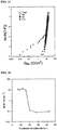
- FIG. 8 shows the results of a TDDB test under a constant current stress performed on 50 samples of the MOS embodiment disclosed above.
- a Weibull graph of FIG. 8 is obtained by plotting a distribution of charge density Q BD per unit area (C/cm 2 ), which has passed through the gate insulating film until a TDDB occurred in the MOS structure according to the first embodiment, as a function of a cumulative failure rate F.
- the gate oxide film of the MOS structure used in this test has a thickness of 12 nm, and the gate electrode has a diameter of 200 ⁇ m.
- An area of the gate electrode is substantially equal to that of known devices (see the test results in Table 1). Also, the stress current in this test is set to be 10 mA/cm 2 .
- FIG. 9 shows a relation between the maximum value of the Q BD life of the MOS structure plotted in FIG. 8 and the current stress J inj .
- the Q BD life is increased exponentially.
- the Q BD is higher than 50 C/cm 2 (Q BD > 50 C/cm 2 ).
- the intensity of the gate electric field of the actual MOS device is about 3 MV/cm at most.
- the current density flowing in the gate oxide film is much smaller than 10 -6 A/m 2 .
- the MOS structure of the first embodiment has a very high Q BD lifespan of more than 50 C/cm 2 , which is higher than the MCTB of known devices, under the stress practically applied to the device.
- FIG. 10 shows a relation between the thickness of the gate oxide film and MCTB (the median of the Q BD lifespan).
- the Q BD distribution of the 50 samples falls within a range of one order of magnitude.
- Table 1 when MCTB was intended to be enhanced, the Q BD distribution tended to be remarkably extended. Such a tendency was disadvantageous in the large-scale MOS structure as yield is decreased.
- the first embodiment described herein enhances MCTB and restrains the extension of the Q BD distribution at the same time. According to the discoveries by the present inventor, similar to the MCTB improvement effect, the Q BD distribution restraining effect appears when the thickness of the gate oxide film is decreased below about 20 nm.
- FIG. 11 shows the results of a case where a film pressure of the gate oxide film is respectively set to 6.8 nm, 8.7 nm and 12.0 nm. As shown in FIG. 11 , optimal characteristics are obtained under the conditions of 8.7 nm and 12.0 nm. However, if the thickness of the gate oxide film is thinner than 8 nm, such as 6.8 nm, the Q BD distribution tends to be gradually extended. However, this result is derived from a case where a total gate area of the MOS structure corresponds to that of the aforementioned test sample, a generally-used size as shown in Table 1. In the case where the total gate area is smaller, this result will be decreased. Accordingly, even when the film thickness is smaller than 8 nm, the preferred characteristics can be obtained.
- a second embodiment is directed to an n-channel type planar power MOS field-effect transistor cell, hereinafter MOSFET.
- MOSFET n-channel type planar power MOS field-effect transistor cell
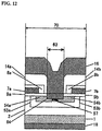
- FIG. 12 is a sectional view showing a chief part of the power MOSFET cell according to the second embodiment.
- a first n- epitaxial layer 2 with a thickness of 10 ⁇ m is grown homoepitaxially on the upper surface of a n + single crystal SiC substrate 1.
- Nitrogen is doped to the first n - epitaxial layer 2 at a concentration of 1 x10 16 /cm 3 .
- the second embodiment can be applied to a substrate, no matter what crystal system the substrate may have, including 4H, 6H, 3C and 15R (H represents a hexagonal system, C represents a cubic system and R represents a rhombohedral system).
- P-base regions 53a and 53b with a predetermined depth, to which a small amount of p-type impurities are doped, are formed at predetermined regions in the surface layer of the n - epitaxial layer 2.
- N + source regions 54a and 54b which have smaller depths than the p-base regions 53a and 53b, are formed in predetermined regions in the surface layer of the p-base regions 53a and 53b.
- the n + source regions 54a and 54b extend from the outer boundaries of the p-base regions 53a and 53b at a predetermined distance.
- a p + base contact region 57 is arranged in the surface layer of the substrate in the middle between the p-base regions 53a and 53b in such a way that the p + base contact region 57 has a smaller depth than each of the p-base regions 53a and 53b and is interposed between the n + source regions 54a and 54b.
- Gate oxide films 9a and 9b are formed selectively on the upper surface of the substrate.
- Polycrystalline Si thermally-oxidized films 8a and 8b are formed on upper portions and side walls of the polycrystalline Si gate electrodes 7a and 7b.
- Interlayer insulating films 14a and 14b are formed on the SiC substrate including the polycrystalline Si thermally-oxidized films 8a and 8b.
- Source window 63 is opened in the interlayer insulating films 14a and 14b.
- the source window 63 is opened in such a way that the source window 63 penetrates through the n + source regions 54a and 54b and the p + base contact region 57.
- a source contact 64 exists at the bottom of the source window 63.
- the source contact 64 is formed by selectively arranging a base material in the form of a thin mental film, such as Ni, at the bottom of the source window 63, and then by alloying the base material with SiC by a rapid thermal annealing.
- the source contact 64 forms its ohmic contact with the n + source regions 54a and 54b and the p + base contact region 57 at the same time.
- the back surface 18 of the substrate is a drain contact, which is formed by the same method as the source contact 64.
- An interconnection 16 connects the source contact 64 with other circuit components on the same substrate or with external circuits through the source window 63.
- the n + SiC substrate 1 is prepared by homoepitaxially growing the n - epitaxial layer 2 on the principal surface of the substrate 1.
- a CVD oxide film 20 with a thickness of 20 nm to 30 nm is deposited on the surface of the n- epitaxial layer 2.
- polycrystalline Si with a thickness of approximately 1.5 ⁇ m (as a material for a mask of an ion implantation process) is formed on the CVD oxide film 20 by a low pressure chemical vapor deposition (LPCVD) method.
- LPCVD low pressure chemical vapor deposition
- SiO 2 , phosphorus silicate glass (PSG) or the like, each of which is formed by a CVD process can be used instead of polycrystalline Si.
- the CVD oxide film 20 can be omitted.
- the polycrystalline Si film on a region where a p-base region is intended to be formed is removed vertically by using a photolithography process and an anisotropic etching process such as a reactive ion etching (RIE) process.
- RIE reactive ion etching
- first ion-implantation masks 21 a and 21 b are formed.
- an etchant gas such as SF 6 is used when the polycrystalline Si film is etched by the RIE process, the thermal oxide film can be etched with a high selective etching ratio. Further, an end point of etching can be detected. Accordingly, plasma-induced damage that would otherwise occur on the upper surface of the substrate, especially on the channel region, can be avoided.
- p-type impurities are ion implanted into the n - epitaxial layer 2, forming the p-base regions 53a and 53b.
- the polycrystalline Si is actually deposited to the back surface of the epitaxial substrate 1, the polycrystalline Si thus deposited is not illustrated in FIG. 13 .
- Examples of conditions under which ions are implanted into the p-base regions 53a and 53b are as follows:
- the CVD oxide film 20 and the first ion-implantation masks 21 a and 21 b are removed by a wet etching process.
- the n + source regions 54a and 54b and the p + base contact region 57 are formed by using the same procedure as the ions have been selectively implanted into the p-base regions 53a and 53b.
- Examples of conditions under which the ions are selectively implanted into the n + source regions 54a and 54b are as follows:
- the substrate is dipped into a mixed solution of hydrofluoric acid and nitric acid.
- a mixed solution of hydrofluoric acid and nitric acid the substrate is dipped into a mixed solution of hydrofluoric acid and nitric acid.
- the substrate can be alternately dipped into a thermal phosphoric acid solution and a BHF solution so that the polycrystalline Si and the SiO 2 are removed sequentially.
- the substrate from which the masks have been removed is cleaned and dried. Thereafter, the substrate is thermally treated in an atmospheric pressure, pure Ar atmosphere at a temperature of 1,700 °C for one minute.
- all of the conductive dopants, which have been ion implanted into the p-base regions 53a and 53b, the n + source regions 54a and 54b and the p + base contact region 57, are activated at once.
- the substrate which has been fully cleaned by using an RCA cleaning process, is thermally oxidized in a dry oxygen atmosphere.
- thermal oxide films are grown on the upper surface and the back surface of the substrate.
- the thermal oxide films are removed by using a buffered hydrofluoric acid solution. It is advantageous that the thickness of each of the sacrificial oxide films is less than 50 nm, advantageously from 5 nm to 20 nm.
- the substrate on which the sacrificial oxidation process has been completed is fully cleaned once again by the RCA cleaning process. Thereafter, a thick insulating film is formed on the upper surface of the substrate by using a thermal oxidation process, a CVD process or the like.
- an element region 70 (shown in FIG. 12 ), from which a field region where the thick oxide film exists and the thick oxide film is removed, is formed by using a generally-known photolithography process and a wet etching process or a dry etching process.
- the shape of the element region 70 in FIG. 12 is different from the shape represented by FIG. 13 , where the element region is not shown. This is because the field region including the lower insulating film 4 and the upper insulating film 5 is formed at the outer portion around the element region by using the same method as the first embodiment.
- the substrate is fully cleaned once again by using the RCA cleaning process.
- the substrate is dipped in a diluted hydrofluoric acid solution for 5 to 10 seconds to remove a chemical oxide film (SiO 2 ) that has been formed on the surface of the element region 70.
- the substrate is completely cleaned of the diluted hydrofluoric acid solution by using ultrapure water and is then dried.
- the substrate is thermally oxidized so that the gate oxide films 9a and 9b are grown on the surface of the substrate in the element region 70. As a result, the structure shown in FIG. 13C is obtained.
- the gate oxidation temperature is set higher than any other heat treatment temperature in the following processes.
- a rapid heating process is later performed at a temperature of 1,000 °C to achieve an ohmic contact between the source contact electrode 64 above the upper surface of the substrate and the drain electrode 17 on the back surface of the substrate.
- 1,160 °C which is higher than the above temperature, is chosen to be the oxidation temperature by example.
- a polycrystalline Si film with a thickness of 300 nm to 400 nm is formed on the entire upper surface and the entire back surface of the substrate by a low pressure CVD process using a silane material at a growth temperature of 600 °C to 700 °C.
- phosphorus (P) is doped to the polycrystalline Si film by a generally well-known thermal diffusion method using phosphorus chloride oxide (POCl 3 ) and oxygen at a processing temperature of 900 °C to 950 °C, providing conductivity.
- the upper surface of the substrate is coated with photoresist.
- the polycrystalline Si film above the upper surface of the substrate is patterned by using a photolithography process and a reactive ion etching (RIE) process, which uses hexafluoroethane C 2 F 6 and oxygen as etchants.
- RIE reactive ion etching
- the gate electrodes 7a and 7b are defined.
- the polycrystalline Si film is also formed on the back surface of the epitaxial substrate 1. However, this polycrystalline Si film is not illustrated in FIG. 14A .
- the SiC epitaxial substrate 1 which has been etched by using the RIE process, is cleaned by an RCA cleaning process and is then dried.
- the SiC epitaxial substrate 1 is oxidized by a wet oxidation process (pyrogenically oxidized) at a temperature of 950 °C.
- the polycrystalline Si thermally-oxidized films 8a and 8b are grown on the upper surfaces and the side surfaces of the polycrystalline Si gate electrodes 7a and 7b.
- the polycrystalline Si thermally-oxidized films 8a and 8b are formed not only on the side walls of the gate electrodes but also on the upper surfaces of the gate electrodes, the thickness of each of the polycrystalline Si gate electrodes is decreased. As such, taking this decrease into consideration, the initial thickness of each of the polycrystalline Si gate electrodes 7a and 7b is defined.
- the interlayer insulating film 14 is deposited on the entire upper surface of the substrate.
- a SiO 2 film (NSG) with a thickness of approximately 1 ⁇ m formed by an atmospheric pressure CVD process using silane and oxygen as materials
- PSG phosphorus silicate glass
- BPSG boron phosphorus silicate glass
- the materials for the interlayer insulating film 14 are not limited to the SiO 2 film, phosphorus silicate glass or boron phosphorus silicate glass. Thereafter, the substrate is put into a generally-used diffusion furnace and is appropriately thermally treated in a N 2 atmosphere for tens of minutes. Thus, the interlayer insulating film 14 is highly dense. The temperature for this heat treatment is appropriately chosen to be lower than the temperature at which the gate insulating film is formed, for example, in a range of 900 °C to 1,000 °C.
- the source window 63 is opened in the interlayer insulating film 14 resulting in insulating films 14a and 14b above the upper surface of the substrate as well as the gate oxide films 9a and 9b by using a generally-known photolithography process and a dry/wet etching process.
- the gate contact window formed at the periphery of the element region is also opened at the same time.
- a thermal oxide film (not shown) on the transitory polycrystalline Si film on the back surface is removed at the same time.
- a base material 25 for the source contact electrode is deposited on the entire upper surface of the substrate, above which the photoresists and the etching masks remain, by using a film formation process such as a DC sputtering process.
- a film formation process such as a DC sputtering process.
- a Ni film, a Co film or the like, with a thickness of 50 nm, can be used as the base material 25 for the source contact electrode.
- the substrate is dipped in a specialized photoresist stripper. As such, the photoresist remaining on the surface of the substrate is completely removed.
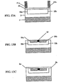
- the substrate structure shown in FIG. 15B is obtained, wherein the base material 25 for the source contact electrode is deposited only on the source window 63 and in the bottom of the gate contact window.
- the substrate is fully cleaned and dried. Thereafter, the entire upper surface of the substrate is-coated with a protective resist material such as photoresist with a thickness of 1 ⁇ m or more. Further, the polycrystalline Si film remaining on the back surface of the substrate is removed by using a dry etching process.
- the protective resist is needed to prevent the base material 25 for the contact electrode and the gate insulating films 14a and 14b from being deteriorated due to plasma-induced damage, electrostatic charge and contamination, which are caused during the dry etching process.
- the substrate 1 is dipped into a buffered hydrofluoric acid solution.
- a transitory thermally-oxidized film (not shown), which has been formed on the back surface during the gate oxidation, is removed.
- a clean crystal plane is exposed at the back surface of the epitaxial substrate 1.
- the substrate is completely cleaned of the buffered hydrofluoric acid solution by using ultrapure water and is dried.
- the substrate is put into a vapor deposition system under a vacuum.
- a desired base material (not shown) for the drain contact electrode is deposited on the back surface of the substrate.
- a Ni film or a Co film with a thickness of 50 nm to 100 nm, can be used as the electrode base material on the back surface.
- the resist which has been used to protect the surface of the substrate, is completely removed by using a specialized stripper solution.
- the SiC epitaxial substrate 1 is fully cleaned, rinsed and dried.
- the substrate 1 is installed in a rapid heating process system.
- the rapid heating process contact annealing process
- each of the base materials (Ni film) for the contact electrodes which has been deposited in the bottom of the source window 63 and the bottom and the back surface of the gate contact window, is alloyed with the n + source regions 54a and 54b [/p + base contact region 57], the polycrystalline Si gate electrode contact region (not shown) and the back surface of the n + SiC substrate. Accordingly, a source contact 64, which is ohmically contacted with an extremely low resistance, a gate contact (not shown) and a drain contact 18 are formed. As a result, a substrate structure shown in FIG. 15C is obtained.
- the substrate, to which the contact annealing process has been applied is installed into a magnetron sputtering system, which is kept in high vacuum. This is so that a desired material for interconnection, for example Al with a thickness of 3 ⁇ m, is deposited on the entire upper surface of the substrate.
- a desired material for interconnection for example Al with a thickness of 3 ⁇ m
- the resist mask is completely removed by using a specialized stripper solution.
- planar power MOSFET cell according to second embodiment (shown in FIG. 12 ) is completed.
- planar power MOSFET cell including the MOS structure according to the embodiments herein demonstrates very preferable transistor characteristics.
- the components of the MOS structure demonstrate the same high reliabilities as the components of the MOS structure according to the first embodiment shown in FIGS. 8 and 9 . That is, the planar power MOSFET cell and its manufacturing method improve the durability against TDDB of the gate oxide film in the SiC thermally-oxidized-filmed MOS gate structure included in a conventional planar power MOSFET. As such, the MCTB value is increased by at least one order of magnitude while simultaneously restraining the extension of the TDDB life distribution, thereby reducing the TDDB-induced defect rate.
- the second embodiment is directed to applying the MOS structure of the embodiment to the planar power MOSFET cell.
- the embodiment can be applied to an insulated gate bipolar transistor (IGBT) cell including an element structure similar to the planar power MOSFET cell.
- IGBT insulated gate bipolar transistor
- the IGBT cell can have the same effects as the planar power MOSFET cell of the second embodiment.
Landscapes
- Insulated Gate Type Field-Effect Transistor (AREA)
- Electrodes Of Semiconductors (AREA)
- Semiconductor Integrated Circuits (AREA)
Claims (8)
- Siliziumcarbid(SiC)-Halbleitervorrichtung mit einer Metalloxid-Halbleiter(MOS)-Struktur, wobei die Vorrichtung:ein SiC-Substrat (1);eine Gate-Elektrode (7), welche aus einem polykristallinen Silizium (Si) hergestellt ist;einen Gate-Oxidfilm (9), welcher durch thermisches Oxidieren des SiC-Substrates (1) ausgebildet wird, wobei der Gate-Oxidfilms (9) zwischen dem SiC-Substrat (1) und der Gate-Elektrode (7) angeordnet ist, und mit dem SiC-Substrat (1) und der Gate Elektrode (7) verbunden ist, wobei die Dicke des Gate-Oxidfilms (9) höchstens 20 nm beträgt;
einen ohmschen Kontakt (17), welcher elektrisch mit dem SiC-Substrat(1) verbunden ist; und einen thermisch oxidierten polykristallinen Siliziumfilm (8), welcher durch Oxidieren einer Oberfläche der Gate-Elektrode (7) gebildet wird, umfasst, wobei
die Siliziumcarbid(SiC)-Halbleitervorrichtung erhalten wird durch:Erhöhen einer Temperatur auf mindestens eine vorbestimmte Temperatur, während das SiC-Substrat (1) in einer Inertgasumgebung aufrechterhalten wird;Aufrechterhalten des SiC-Substrats (1) in einer Inertgasumgebung;Ausbilden des Gate-Oxidfilms (9) durch thermisches Oxidieren des SiC-Substrats (1) durch Zuführung eines Oxidationsgases, wenn die Temperatur mindestens auf eine vorbestimmte Temperatur steigt;Beenden der Zuführung eines Oxidationsgases und Wiederherstellen der Inertgasumgebung, wenn eine Dicke des Gate-Oxidfilms (9) eine vorbestimmte Dicke erreicht;Verringern der Temperatur und Beenden der thermischen Oxidation des SiC-Substrats (1), wenn die Inertgasumgebung wiederhergestellt ist, undAusbilden der Gate-Elektrode (7) auf einer Oberfläche des Gate-Oxidfilms (9) durch Abscheiden des polykristallinen Siliziums auf dem Gate-Oxidfilm (9),wobei das thermische Oxidieren des SiC-Substrates (1) bei einer Temperatur, welche höher als jede andere Temperatur in den folgenden Verfahrensschritten ist, durchgeführt wird,ferner umfassend ein Ausbilden eines thermisch oxidierten polykristallinen Siliziumfilms (8) durch Oxidieren eines Teils der Oberfläche der Gate-Elektrode (7); und:Ausbilden eines Zwischenschicht-Isolationsfilms (14) auf dem Gate-Oxidfilm (9) und dem thermisch oxidierten polykristallinen Siliziumfilm (8); oderAusbilden eines Zwischenschicht-Isolationsfilms (14) auf einem thermisch oxidierten polykristallinen Siliziumfilm (8) und einem freiliegenden Teil des Gate-Oxidfilms (9) und/oder eines Feld-Isolationsfilms (3). - Siliziumcarbid(SiC)-Halbleitervorrichtung nach Anspruch 1, wobei die Dicke des Gate-Oxidfilms (9) höchstens 15 nm beträgt.
- Siliziumcarbid(SiC)-Halbleitervorrichtung nach Anspruch 2, wobei die Dicke des Gate-Oxidfilms (9) zwischen 8 nm und 15 nm beträgt.
- Siliziumcarbid(SiC)-Halbleitervorrichtung nach Anspruch 1 ferner umfassend:einen unteren Isolationsfilm (4), welcher durch thermisches Oxidieren des SiC-Substrates (1) ausgebildet wird;einen oberen Isolationsfilm (5), welcher auf den unteren Isolationsfilm (4) aufgetragen ist, wobei der obere Isolationsfilm (5) durch ein von der thermischen Oxidation verschiedenes Verfahren ausgebildet wird, und der obere Isolationsfilm (5) und der untere Isolationsfilm (4) den Feld-Isolationsfilm (3) bilden; undein Gate-Fenster (6), welches in dem Feld-Isolationsfilm (3) ausgebildet ist, wobei der Gate-Oxidfilm (9) in dem Gate-Fenster (6) zwischen dem SiC-Substrat(1) und der Gate-Elektrode (7) ausgebildet ist.
- Siliziumcarbid(SiC)-Halbleitervorrichtung nach Anspruch 4, wobei die Gate-Elektrode (7) auf dem Gate-Oxidfilm (9) innerhalb des Gate-Fensters (6) und auf einem Teil des Feld-Isolationsfilms (3) abgeschieden ist.
- Siliziumcarbid(SiC)-Halbleitervorrichtung nach Anspruch 5, wobei der Zwischenschicht-Isolationsfilm (14) auf dem Gate-Oxidfilm (9) und dem thermisch oxidierten polykristallinen Siliziumfilm (8) ausgebildet ist.
- Siliziumcarbid(SiC)-Halbleitervorrichtung nach Anspruch 5, wobei der Zwischenschicht-Isolationsfilm (14) auf dem thermisch oxidierten polykristallinen Film (8) und einem Teil des Feld-Isolationsfilms (3) ausgebildet ist.
- Siliziumcarbid(SiC)-Halbleitervorrichtung nach Anspruch 4, wobei der obere Isolationsfilm (5) eine Dicke von 400 nm aufweist.
Applications Claiming Priority (2)
| Application Number | Priority Date | Filing Date | Title |
|---|---|---|---|
| JP2007068572A JP4793293B2 (ja) | 2007-03-16 | 2007-03-16 | 炭化珪素半導体装置及びその製造方法 |
| EP08152760.8A EP1970945B1 (de) | 2007-03-16 | 2008-03-14 | Verfahren zum Herstellen einer Siliciumkarbid-Halbleitervorrichtung |
Related Parent Applications (3)
| Application Number | Title | Priority Date | Filing Date |
|---|---|---|---|
| EP08152760.8A Division EP1970945B1 (de) | 2007-03-16 | 2008-03-14 | Verfahren zum Herstellen einer Siliciumkarbid-Halbleitervorrichtung |
| EP08152760.8A Division-Into EP1970945B1 (de) | 2007-03-16 | 2008-03-14 | Verfahren zum Herstellen einer Siliciumkarbid-Halbleitervorrichtung |
| EP08152760.8 Division | 2008-03-14 |
Publications (2)
| Publication Number | Publication Date |
|---|---|
| EP2284867A1 EP2284867A1 (de) | 2011-02-16 |
| EP2284867B1 true EP2284867B1 (de) | 2018-05-09 |
Family
ID=39400934
Family Applications (2)
| Application Number | Title | Priority Date | Filing Date |
|---|---|---|---|
| EP10014514.3A Ceased EP2284867B1 (de) | 2007-03-16 | 2008-03-14 | Siliciumkarbid-Halbleitervorrichtung |
| EP08152760.8A Ceased EP1970945B1 (de) | 2007-03-16 | 2008-03-14 | Verfahren zum Herstellen einer Siliciumkarbid-Halbleitervorrichtung |
Family Applications After (1)
| Application Number | Title | Priority Date | Filing Date |
|---|---|---|---|
| EP08152760.8A Ceased EP1970945B1 (de) | 2007-03-16 | 2008-03-14 | Verfahren zum Herstellen einer Siliciumkarbid-Halbleitervorrichtung |
Country Status (5)
| Country | Link |
|---|---|
| US (2) | US7772058B2 (de) |
| EP (2) | EP2284867B1 (de) |
| JP (1) | JP4793293B2 (de) |
| KR (1) | KR100946422B1 (de) |
| CN (2) | CN101635313A (de) |
Families Citing this family (26)
| Publication number | Priority date | Publication date | Assignee | Title |
|---|---|---|---|---|
| IT1392577B1 (it) | 2008-12-30 | 2012-03-09 | St Microelectronics Rousset | Processo di fabbricazione di un dispositivo elettronico di potenza integrato in un substrato semiconduttore ad ampio intervallo di banda proibita e dispositivo elettronico cosi' ottenuto |
| WO2010098294A1 (ja) | 2009-02-24 | 2010-09-02 | 三菱電機株式会社 | 炭化珪素半導体装置 |
| JP5633328B2 (ja) * | 2010-11-18 | 2014-12-03 | 住友電気工業株式会社 | 半導体装置の製造方法 |
| CN102543704B (zh) * | 2010-12-31 | 2014-04-02 | 中芯国际集成电路制造(上海)有限公司 | 栅极氧化层的形成方法 |
| JP5655570B2 (ja) * | 2011-01-06 | 2015-01-21 | 住友電気工業株式会社 | 半導体装置の製造方法 |
| CN102810465B (zh) * | 2011-06-02 | 2015-09-30 | 中国科学院微电子研究所 | 一种在SiC材料上生长SiO2钝化层的方法 |
| JP5704003B2 (ja) * | 2011-07-15 | 2015-04-22 | 住友電気工業株式会社 | 半導体装置の製造方法 |
| CN104170058B (zh) * | 2011-11-23 | 2017-08-08 | 阿科恩科技公司 | 通过插入界面原子单层改进与iv族半导体的金属接触 |
| TW201324587A (zh) * | 2011-12-15 | 2013-06-16 | 國立交通大學 | 半導體元件及其製作方法 |
| JP5914060B2 (ja) * | 2012-03-09 | 2016-05-11 | 三菱電機株式会社 | 炭化珪素半導体装置の製造方法 |
| JP6029397B2 (ja) * | 2012-09-14 | 2016-11-24 | 三菱電機株式会社 | 炭化珪素半導体装置 |
| US9269765B2 (en) * | 2013-10-21 | 2016-02-23 | Panasonic Intellectual Property Management Co., Ltd. | Semiconductor device having gate wire disposed on roughened field insulating film |
| CN103972071A (zh) * | 2014-04-22 | 2014-08-06 | 上海华力微电子有限公司 | 含氮栅极氧化层的制作方法 |
| JP6284840B2 (ja) * | 2014-06-26 | 2018-02-28 | ルネサスエレクトロニクス株式会社 | 半導体装置の製造方法および半導体装置 |
| KR101964153B1 (ko) * | 2014-08-28 | 2019-04-03 | 한국전기연구원 | 절연 또는 반절연 SiC 기판에 구현된 SiC 반도체 소자 및 그 제조 방법 |
| DE112016002263T5 (de) * | 2015-05-18 | 2018-03-01 | Sumitomo Electric Industries, Ltd. | Verfahren zur Herstellung eines Silizium-Epitaxiesubstrats, Siliziumkarbid-Epitaxiesubstrat, Verfahren zur Herstellung einer Siliziumkarbid-Halbleitervorrichtung und Siliziumkarbid-Halbleitervorrichtung |
| CN104966735A (zh) | 2015-05-26 | 2015-10-07 | 株洲南车时代电气股份有限公司 | 一种碳化硅mosfet器件及其制备方法 |
| DE102016112877B4 (de) * | 2015-09-07 | 2021-07-15 | Fuji Electric Co., Ltd. | Verfahren zum Herstellen einer Halbleitervorrichtung und für das Verfahren verwendete Halbleiterherstellungsvorrichtung |
| JP6436024B2 (ja) * | 2015-09-14 | 2018-12-12 | 住友電気工業株式会社 | 炭化珪素エピタキシャル基板の製造方法 |
| CN106019762B (zh) | 2016-07-27 | 2019-05-07 | 深圳市华星光电技术有限公司 | 一种裸眼3d透镜显示设备及其制作方法 |
| CN106653596B (zh) * | 2016-12-28 | 2019-05-31 | 东方环晟光伏(江苏)有限公司 | 一种湿法刻蚀工艺中去磷硅玻璃槽的配置方法 |
| JP6861365B2 (ja) | 2017-08-29 | 2021-04-21 | パナソニックIpマネジメント株式会社 | 炭化珪素半導体装置およびその製造方法 |
| CN109979798B (zh) * | 2017-12-27 | 2022-02-25 | 无锡华润微电子有限公司 | 碳化硅晶圆湿法腐蚀方法 |
| KR102340307B1 (ko) * | 2020-04-09 | 2021-12-15 | 포항공과대학교 산학협력단 | 4H-SiC 기판에 옴 접촉을 형성하는 반도체 및 그것의 제조 방법 |
| DE112020007758T5 (de) * | 2020-11-06 | 2023-08-17 | Mitsubishi Electric Corporation | Halbleitereinheit und leistungswandlereinheit |
| KR102750672B1 (ko) * | 2023-12-04 | 2025-01-09 | (주) 예스티 | SiC 반도체 기판의 고압 산화 방법 및 장치 |
Citations (2)
| Publication number | Priority date | Publication date | Assignee | Title |
|---|---|---|---|---|
| US20020038891A1 (en) * | 2000-10-03 | 2002-04-04 | Sei-Hyung Ryu | Silicon carbide power metal-oxide semiconductor field effect transistors having a shorting channel and methods of fabricating silicon carbide metal-oxide semiconductor field effect transistors having a shorting channel |
| WO2006115148A1 (ja) * | 2005-04-22 | 2006-11-02 | Bridgestone Corporation | 炭化ケイ素単結晶ウェハ及びその製造方法 |
Family Cites Families (16)
| Publication number | Priority date | Publication date | Assignee | Title |
|---|---|---|---|---|
| JP3433041B2 (ja) * | 1996-03-13 | 2003-08-04 | 株式会社東芝 | 半導体装置 |
| JP3893725B2 (ja) * | 1998-03-25 | 2007-03-14 | 株式会社デンソー | 炭化珪素半導体装置の製造方法 |
| JP3460585B2 (ja) * | 1998-07-07 | 2003-10-27 | 富士電機株式会社 | 炭化けい素mos半導体素子の製造方法 |
| JP3551909B2 (ja) * | 1999-11-18 | 2004-08-11 | 株式会社デンソー | 炭化珪素半導体装置の製造方法 |
| JP3881840B2 (ja) | 2000-11-14 | 2007-02-14 | 独立行政法人産業技術総合研究所 | 半導体装置 |
| JP2003031571A (ja) | 2001-07-12 | 2003-01-31 | Nissan Motor Co Ltd | 炭化珪素半導体の酸化膜の形成方法 |
| JP4525958B2 (ja) * | 2001-08-27 | 2010-08-18 | 独立行政法人産業技術総合研究所 | 半導体装置の製造方法 |
| US7092868B2 (en) * | 2001-10-30 | 2006-08-15 | International Business Machines Corporation | Annealing harvest event testcase collection within a batch simulation farm |
| JP3559971B2 (ja) * | 2001-12-11 | 2004-09-02 | 日産自動車株式会社 | 炭化珪素半導体装置およびその製造方法 |
| JP3950959B2 (ja) * | 2002-06-28 | 2007-08-01 | 独立行政法人産業技術総合研究所 | 半導体装置の製造方法 |
| JP4016954B2 (ja) * | 2004-02-03 | 2007-12-05 | 三菱電機株式会社 | 炭化珪素半導体装置の製造方法 |
| JP2006074024A (ja) * | 2004-08-04 | 2006-03-16 | Nissan Motor Co Ltd | 炭化珪素半導体装置及びその製造方法 |
| JP4742545B2 (ja) * | 2004-09-09 | 2011-08-10 | 日産自動車株式会社 | 炭化珪素半導体装置の製造方法 |
| KR100619603B1 (ko) * | 2005-01-07 | 2006-09-11 | 한국전기연구원 | 이중산화막을 갖는 고내압 탄화규소 쇼트키 다이오드 소자및 그 제조방법 |
| JP2007066944A (ja) * | 2005-08-29 | 2007-03-15 | Nissan Motor Co Ltd | 炭化珪素半導体装置及びその製造方法 |
| JP2007068572A (ja) | 2005-09-02 | 2007-03-22 | Ngk Spark Plug Co Ltd | 酸素濃縮器用治具及び酸素濃縮器 |
-
2007
- 2007-03-16 JP JP2007068572A patent/JP4793293B2/ja not_active Expired - Fee Related
-
2008
- 2008-01-30 US US12/022,607 patent/US7772058B2/en not_active Expired - Fee Related
- 2008-03-14 KR KR1020080023589A patent/KR100946422B1/ko not_active Expired - Fee Related
- 2008-03-14 EP EP10014514.3A patent/EP2284867B1/de not_active Ceased
- 2008-03-14 CN CN200910163147A patent/CN101635313A/zh active Pending
- 2008-03-14 CN CNA200810084721XA patent/CN101266929A/zh active Pending
- 2008-03-14 EP EP08152760.8A patent/EP1970945B1/de not_active Ceased
-
2010
- 2010-07-15 US US12/837,408 patent/US20100276703A1/en not_active Abandoned
Patent Citations (2)
| Publication number | Priority date | Publication date | Assignee | Title |
|---|---|---|---|---|
| US20020038891A1 (en) * | 2000-10-03 | 2002-04-04 | Sei-Hyung Ryu | Silicon carbide power metal-oxide semiconductor field effect transistors having a shorting channel and methods of fabricating silicon carbide metal-oxide semiconductor field effect transistors having a shorting channel |
| WO2006115148A1 (ja) * | 2005-04-22 | 2006-11-02 | Bridgestone Corporation | 炭化ケイ素単結晶ウェハ及びその製造方法 |
Also Published As
| Publication number | Publication date |
|---|---|
| EP1970945A3 (de) | 2009-07-01 |
| CN101635313A (zh) | 2010-01-27 |
| KR20080084695A (ko) | 2008-09-19 |
| KR100946422B1 (ko) | 2010-03-10 |
| JP4793293B2 (ja) | 2011-10-12 |
| US20100276703A1 (en) | 2010-11-04 |
| EP1970945A2 (de) | 2008-09-17 |
| US20080227256A1 (en) | 2008-09-18 |
| EP2284867A1 (de) | 2011-02-16 |
| CN101266929A (zh) | 2008-09-17 |
| US7772058B2 (en) | 2010-08-10 |
| JP2008235331A (ja) | 2008-10-02 |
| EP1970945B1 (de) | 2018-05-09 |
Similar Documents
| Publication | Publication Date | Title |
|---|---|---|
| EP1970945B1 (de) | Verfahren zum Herstellen einer Siliciumkarbid-Halbleitervorrichtung | |
| US6841436B2 (en) | Method of fabricating SiC semiconductor device | |
| KR100980527B1 (ko) | 탄화 규소 반도체 장치 및 그 제조 방법 | |
| EP1566843B1 (de) | Herstellungsverfahren eines siliziumkarbid-halbleiterbauelements | |
| US6764963B2 (en) | Manufacturing method of semiconductor devices | |
| US8252672B2 (en) | Silicon carbide semiconductor device comprising silicon carbide layer and method of manufacturing the same | |
| US7510977B2 (en) | Method for manufacturing silicon carbide semiconductor device | |
| JP3987796B2 (ja) | N2oを用いた、炭化ケイ素層上への酸化物層の製造方法 | |
| JP4872217B2 (ja) | 炭化珪素半導体素子の製造方法 | |
| CN101174569A (zh) | 制造碳化硅半导体器件的方法 | |
| JP2005166930A (ja) | SiC−MISFET及びその製造方法 | |
| JP4483179B2 (ja) | 半導体装置の製造方法 | |
| US7994035B2 (en) | Semiconductor device fabricating method including thermal oxidation of a substrate, forming a second oxide, and thermal processing a gate electrode | |
| JP5229845B2 (ja) | 炭化ケイ素mosfetの製造方法および炭化ケイ素mosfet | |
| JP4842527B2 (ja) | 半導体装置の製造方法 | |
| CN108257861A (zh) | 一种栅氧化层的制备方法及mos功率器件 | |
| US20060027833A1 (en) | Silicon carbide semiconductor device and method of manufacturing the same | |
| JP5460768B2 (ja) | 炭化珪素半導体装置の製造方法 | |
| JP2021082689A (ja) | 炭化珪素半導体装置および炭化珪素半導体装置の製造方法 | |
| JP5360011B2 (ja) | 炭化珪素半導体装置の製造方法 | |
| JP2006074024A (ja) | 炭化珪素半導体装置及びその製造方法 | |
| JP2025007323A (ja) | 炭化珪素半導体装置の製造方法 |
Legal Events
| Date | Code | Title | Description |
|---|---|---|---|
| PUAI | Public reference made under article 153(3) epc to a published international application that has entered the european phase |
Free format text: ORIGINAL CODE: 0009012 |
|
| 17P | Request for examination filed |
Effective date: 20101111 |
|
| AC | Divisional application: reference to earlier application |
Ref document number: 1970945 Country of ref document: EP Kind code of ref document: P |
|
| AK | Designated contracting states |
Kind code of ref document: A1 Designated state(s): DE FR GB |
|
| 17Q | First examination report despatched |
Effective date: 20160426 |
|
| GRAP | Despatch of communication of intention to grant a patent |
Free format text: ORIGINAL CODE: EPIDOSNIGR1 |
|
| RIC1 | Information provided on ipc code assigned before grant |
Ipc: H01L 29/94 20060101ALN20171109BHEP Ipc: H01L 29/417 20060101ALN20171109BHEP Ipc: H01L 29/78 20060101ALI20171109BHEP Ipc: H01L 29/45 20060101ALN20171109BHEP Ipc: H01L 29/66 20060101ALI20171109BHEP Ipc: H01L 29/739 20060101ALN20171109BHEP Ipc: H01L 21/04 20060101AFI20171109BHEP |
|
| INTG | Intention to grant announced |
Effective date: 20171122 |
|
| GRAS | Grant fee paid |
Free format text: ORIGINAL CODE: EPIDOSNIGR3 |
|
| GRAA | (expected) grant |
Free format text: ORIGINAL CODE: 0009210 |
|
| AC | Divisional application: reference to earlier application |
Ref document number: 1970945 Country of ref document: EP Kind code of ref document: P |
|
| AK | Designated contracting states |
Kind code of ref document: B1 Designated state(s): DE FR GB |
|
| REG | Reference to a national code |
Ref country code: GB Ref legal event code: FG4D |
|
| REG | Reference to a national code |
Ref country code: DE Ref legal event code: R096 Ref document number: 602008055220 Country of ref document: DE |
|
| REG | Reference to a national code |
Ref country code: DE Ref legal event code: R097 Ref document number: 602008055220 Country of ref document: DE |
|
| PLBE | No opposition filed within time limit |
Free format text: ORIGINAL CODE: 0009261 |
|
| STAA | Information on the status of an ep patent application or granted ep patent |
Free format text: STATUS: NO OPPOSITION FILED WITHIN TIME LIMIT |
|
| 26N | No opposition filed |
Effective date: 20190212 |
|
| PGFP | Annual fee paid to national office [announced via postgrant information from national office to epo] |
Ref country code: GB Payment date: 20190313 Year of fee payment: 12 Ref country code: DE Payment date: 20190226 Year of fee payment: 12 |
|
| PGFP | Annual fee paid to national office [announced via postgrant information from national office to epo] |
Ref country code: FR Payment date: 20190213 Year of fee payment: 12 |
|
| REG | Reference to a national code |
Ref country code: DE Ref legal event code: R119 Ref document number: 602008055220 Country of ref document: DE |
|
| PG25 | Lapsed in a contracting state [announced via postgrant information from national office to epo] |
Ref country code: DE Free format text: LAPSE BECAUSE OF NON-PAYMENT OF DUE FEES Effective date: 20201001 Ref country code: FR Free format text: LAPSE BECAUSE OF NON-PAYMENT OF DUE FEES Effective date: 20200331 |
|
| GBPC | Gb: european patent ceased through non-payment of renewal fee |
Effective date: 20200314 |
|
| PG25 | Lapsed in a contracting state [announced via postgrant information from national office to epo] |
Ref country code: GB Free format text: LAPSE BECAUSE OF NON-PAYMENT OF DUE FEES Effective date: 20200314 |