EP2284881A1 - Boîtier de stockage haute fréquence et module haute fréquence - Google Patents
Boîtier de stockage haute fréquence et module haute fréquence Download PDFInfo
- Publication number
- EP2284881A1 EP2284881A1 EP09746417A EP09746417A EP2284881A1 EP 2284881 A1 EP2284881 A1 EP 2284881A1 EP 09746417 A EP09746417 A EP 09746417A EP 09746417 A EP09746417 A EP 09746417A EP 2284881 A1 EP2284881 A1 EP 2284881A1
- Authority
- EP
- European Patent Office
- Prior art keywords
- high frequency
- earth conductor
- circuits
- cavity
- circuit
- Prior art date
- Legal status (The legal status is an assumption and is not a legal conclusion. Google has not performed a legal analysis and makes no representation as to the accuracy of the status listed.)
- Granted
Links
Images


Classifications
-
- H—ELECTRICITY
- H10—SEMICONDUCTOR DEVICES; ELECTRIC SOLID-STATE DEVICES NOT OTHERWISE PROVIDED FOR
- H10W—GENERIC PACKAGES, INTERCONNECTIONS, CONNECTORS OR OTHER CONSTRUCTIONAL DETAILS OF DEVICES COVERED BY CLASS H10
- H10W76/00—Containers; Fillings or auxiliary members therefor; Seals
- H10W76/10—Containers or parts thereof
- H10W76/12—Containers or parts thereof characterised by their shape
- H10W76/13—Containers comprising a conductive base serving as an interconnection
-
- H—ELECTRICITY
- H01—ELECTRIC ELEMENTS
- H01P—WAVEGUIDES; RESONATORS, LINES, OR OTHER DEVICES OF THE WAVEGUIDE TYPE
- H01P3/00—Waveguides; Transmission lines of the waveguide type
- H01P3/12—Hollow waveguides
- H01P3/121—Hollow waveguides integrated in a substrate
-
- H—ELECTRICITY
- H10—SEMICONDUCTOR DEVICES; ELECTRIC SOLID-STATE DEVICES NOT OTHERWISE PROVIDED FOR
- H10W—GENERIC PACKAGES, INTERCONNECTIONS, CONNECTORS OR OTHER CONSTRUCTIONAL DETAILS OF DEVICES COVERED BY CLASS H10
- H10W42/00—Arrangements for protection of devices
- H10W42/20—Arrangements for protection of devices protecting against electromagnetic or particle radiation, e.g. light, X-rays, gamma-rays or electrons
-
- H—ELECTRICITY
- H10—SEMICONDUCTOR DEVICES; ELECTRIC SOLID-STATE DEVICES NOT OTHERWISE PROVIDED FOR
- H10W—GENERIC PACKAGES, INTERCONNECTIONS, CONNECTORS OR OTHER CONSTRUCTIONAL DETAILS OF DEVICES COVERED BY CLASS H10
- H10W42/00—Arrangements for protection of devices
- H10W42/20—Arrangements for protection of devices protecting against electromagnetic or particle radiation, e.g. light, X-rays, gamma-rays or electrons
- H10W42/261—Arrangements for protection of devices protecting against electromagnetic or particle radiation, e.g. light, X-rays, gamma-rays or electrons characterised by their shapes or dispositions
- H10W42/267—Patterned shielding planes
-
- H—ELECTRICITY
- H10—SEMICONDUCTOR DEVICES; ELECTRIC SOLID-STATE DEVICES NOT OTHERWISE PROVIDED FOR
- H10W—GENERIC PACKAGES, INTERCONNECTIONS, CONNECTORS OR OTHER CONSTRUCTIONAL DETAILS OF DEVICES COVERED BY CLASS H10
- H10W44/00—Electrical arrangements for controlling or matching impedance
- H10W44/20—Electrical arrangements for controlling or matching impedance at high-frequency [HF] or radio frequency [RF]
-
- G—PHYSICS
- G01—MEASURING; TESTING
- G01S—RADIO DIRECTION-FINDING; RADIO NAVIGATION; DETERMINING DISTANCE OR VELOCITY BY USE OF RADIO WAVES; LOCATING OR PRESENCE-DETECTING BY USE OF THE REFLECTION OR RERADIATION OF RADIO WAVES; ANALOGOUS ARRANGEMENTS USING OTHER WAVES
- G01S7/00—Details of systems according to groups G01S13/00, G01S15/00, G01S17/00
- G01S7/02—Details of systems according to groups G01S13/00, G01S15/00, G01S17/00 of systems according to group G01S13/00
- G01S7/027—Constructional details of housings, e.g. form, type, material or ruggedness
- G01S7/028—Miniaturisation, e.g. surface mounted device [SMD] packaging or housings
-
- H—ELECTRICITY
- H01—ELECTRIC ELEMENTS
- H01P—WAVEGUIDES; RESONATORS, LINES, OR OTHER DEVICES OF THE WAVEGUIDE TYPE
- H01P3/00—Waveguides; Transmission lines of the waveguide type
- H01P3/16—Dielectric waveguides, i.e. without a longitudinal conductor
-
- H—ELECTRICITY
- H01—ELECTRIC ELEMENTS
- H01P—WAVEGUIDES; RESONATORS, LINES, OR OTHER DEVICES OF THE WAVEGUIDE TYPE
- H01P5/00—Coupling devices of the waveguide type
- H01P5/08—Coupling devices of the waveguide type for linking dissimilar lines or devices
- H01P5/10—Coupling devices of the waveguide type for linking dissimilar lines or devices for coupling balanced lines or devices with unbalanced lines or devices
- H01P5/107—Hollow-waveguide/strip-line transitions
-
- H—ELECTRICITY
- H10—SEMICONDUCTOR DEVICES; ELECTRIC SOLID-STATE DEVICES NOT OTHERWISE PROVIDED FOR
- H10W—GENERIC PACKAGES, INTERCONNECTIONS, CONNECTORS OR OTHER CONSTRUCTIONAL DETAILS OF DEVICES COVERED BY CLASS H10
- H10W44/00—Electrical arrangements for controlling or matching impedance
- H10W44/20—Electrical arrangements for controlling or matching impedance at high-frequency [HF] or radio frequency [RF]
- H10W44/203—Electrical connections
- H10W44/209—Vertical interconnections, e.g. vias
-
- H—ELECTRICITY
- H10—SEMICONDUCTOR DEVICES; ELECTRIC SOLID-STATE DEVICES NOT OTHERWISE PROVIDED FOR
- H10W—GENERIC PACKAGES, INTERCONNECTIONS, CONNECTORS OR OTHER CONSTRUCTIONAL DETAILS OF DEVICES COVERED BY CLASS H10
- H10W44/00—Electrical arrangements for controlling or matching impedance
- H10W44/20—Electrical arrangements for controlling or matching impedance at high-frequency [HF] or radio frequency [RF]
- H10W44/203—Electrical connections
- H10W44/216—Waveguides, e.g. strip lines
-
- H—ELECTRICITY
- H10—SEMICONDUCTOR DEVICES; ELECTRIC SOLID-STATE DEVICES NOT OTHERWISE PROVIDED FOR
- H10W—GENERIC PACKAGES, INTERCONNECTIONS, CONNECTORS OR OTHER CONSTRUCTIONAL DETAILS OF DEVICES COVERED BY CLASS H10
- H10W44/00—Electrical arrangements for controlling or matching impedance
- H10W44/20—Electrical arrangements for controlling or matching impedance at high-frequency [HF] or radio frequency [RF]
- H10W44/255—Electrical arrangements for controlling or matching impedance at high-frequency [HF] or radio frequency [RF] for operation at multiple different frequencies
-
- H—ELECTRICITY
- H10—SEMICONDUCTOR DEVICES; ELECTRIC SOLID-STATE DEVICES NOT OTHERWISE PROVIDED FOR
- H10W—GENERIC PACKAGES, INTERCONNECTIONS, CONNECTORS OR OTHER CONSTRUCTIONAL DETAILS OF DEVICES COVERED BY CLASS H10
- H10W72/00—Interconnections or connectors in packages
- H10W72/50—Bond wires
- H10W72/551—Materials of bond wires
- H10W72/552—Materials of bond wires comprising metals or metalloids, e.g. silver
-
- H—ELECTRICITY
- H10—SEMICONDUCTOR DEVICES; ELECTRIC SOLID-STATE DEVICES NOT OTHERWISE PROVIDED FOR
- H10W—GENERIC PACKAGES, INTERCONNECTIONS, CONNECTORS OR OTHER CONSTRUCTIONAL DETAILS OF DEVICES COVERED BY CLASS H10
- H10W72/00—Interconnections or connectors in packages
- H10W72/50—Bond wires
- H10W72/551—Materials of bond wires
- H10W72/552—Materials of bond wires comprising metals or metalloids, e.g. silver
- H10W72/5522—Materials of bond wires comprising metals or metalloids, e.g. silver comprising gold [Au]
-
- H—ELECTRICITY
- H10—SEMICONDUCTOR DEVICES; ELECTRIC SOLID-STATE DEVICES NOT OTHERWISE PROVIDED FOR
- H10W—GENERIC PACKAGES, INTERCONNECTIONS, CONNECTORS OR OTHER CONSTRUCTIONAL DETAILS OF DEVICES COVERED BY CLASS H10
- H10W72/00—Interconnections or connectors in packages
- H10W72/851—Dispositions of multiple connectors or interconnections
- H10W72/874—On different surfaces
- H10W72/884—Die-attach connectors and bond wires
-
- H—ELECTRICITY
- H10—SEMICONDUCTOR DEVICES; ELECTRIC SOLID-STATE DEVICES NOT OTHERWISE PROVIDED FOR
- H10W—GENERIC PACKAGES, INTERCONNECTIONS, CONNECTORS OR OTHER CONSTRUCTIONAL DETAILS OF DEVICES COVERED BY CLASS H10
- H10W90/00—Package configurations
- H10W90/701—Package configurations characterised by the relative positions of pads or connectors relative to package parts
- H10W90/731—Package configurations characterised by the relative positions of pads or connectors relative to package parts of die-attach connectors
- H10W90/734—Package configurations characterised by the relative positions of pads or connectors relative to package parts of die-attach connectors between a chip and a stacked insulating package substrate, interposer or RDL
-
- H—ELECTRICITY
- H10—SEMICONDUCTOR DEVICES; ELECTRIC SOLID-STATE DEVICES NOT OTHERWISE PROVIDED FOR
- H10W—GENERIC PACKAGES, INTERCONNECTIONS, CONNECTORS OR OTHER CONSTRUCTIONAL DETAILS OF DEVICES COVERED BY CLASS H10
- H10W90/00—Package configurations
- H10W90/701—Package configurations characterised by the relative positions of pads or connectors relative to package parts
- H10W90/751—Package configurations characterised by the relative positions of pads or connectors relative to package parts of bond wires
- H10W90/754—Package configurations characterised by the relative positions of pads or connectors relative to package parts of bond wires between a chip and a stacked insulating package substrate, interposer or RDL
Definitions
- the present invention relates to a high frequency storing case and a high frequency module including a cavity, which is a space electromagnetically shielded by a multilayer dielectric substrate on which a plurality of high frequency circuits are mounted, and a shield cover member that covers the multilayer dielectric substrate.
- the high frequency circuits are often mounted in a cavity electrically shielded by a metal frame or the like, in view of stability in the operation, EMI (radiated spurious) standard and the like.
- a package assembly is divided by a seal ring or individual cover member into a plurality of sections (cavities), the semiconductor chips are mounted on each of the divided sections with respect to each function, and the semiconductor chips on the sections are electrically connected by using a feedthrough.
- Patent Document 1 Japanese Patent Application Laid-open No. H10-41421
- this conventional package structure has many problems related to costs and reliability including increase in the number of members such as the seal ring and the cover, and complicated manufacturing steps such as soldering to the package and welding of the cover.
- the chip size is of the order of the wavelength (to about 1 millimeter). Accordingly, shielding or sectioning in a cavity physical dimension that provides substantial cutoff cannot be realized, which requires use of an expensive absorber such as a resistor or a magnetic body.
- a package structure or a module structure in a simple configuration that can ensure isolation also in the high frequency band such as the microwave band and the millimeter band has been desired.
- the present invention has been achieved in view of the above circumstances, and an object of the present invention is to obtain a high frequency storing case and a high frequency module that can ensure spatial isolation between plural high frequency circuits with an inexpensive and simple configuration using a single cavity.
- a high frequency storing case stores therein a plurality of high frequency circuits to be mounted on a multilayer dielectric substrate, and includes a cavity that is formed at least by an electromagnetic shield that is obtained by electrically connecting an earth conductor that is formed on the multilayer dielectric substrate and on which the plural high frequency circuits arranged in a signal propagation direction are mounted, and a shield cover member that spatially covers the plural high frequency circuits, and that has a length in a direction perpendicular to an arrangement direction of the plural high frequency circuits, smaller than 1/2 of an effective wavelength in the substrate of a first signal wave generated by the high frequency circuit, a waveguide aperture that is formed on the earth conductor on which the high frequency circuits are mounted and that is electrically coupled to the cavity, and an end-short-circuited dielectric waveguide that is connected to the waveguide aperture, is formed in a direction of layer lamination of the multilayer dielectric substrate, and has a length approximately 1/4 of an effective wavelength in the substrate
- the waveguide aperture and the end-short-circuited dielectric waveguide are included, and the waveguide aperture and the end-short-circuited dielectric waveguide are caused to operate as a reflection circuit for signals that propagate through the cavity. Therefore, spatial isolation between the plural high frequency circuits can be ensured by an inexpensive and simple configuration using the single cavity.
- FIGS. 1 to 3 depict a configuration of a high frequency module according to an embodiment of the present invention.
- a high frequency module 1 On a high frequency module 1, a plurality of high frequency circuits that operate at a high frequency band such as the microwave band or the millimeter band are mounted.
- the high frequency module 1 is favorably applied to an FM-CW (frequency modulated continuous-wave) radar, for example. It can be also used for a communication device or a microwave radar.
- FM-CW frequency modulated continuous-wave
- an oscillating circuit 10 that generates a high frequency signal of a frequency f0, an amplifying circuit 11 that amplifies an output from the oscillating circuit 10, a multiplying and amplifying circuit 12 that multiplying an output from the amplifying circuit 11 by N (N ⁇ 2), amplifies a multiplied signal of a frequency N ⁇ f0, and outputs the amplified signal and the like are mounted as the high frequency circuits.
- the high frequency circuits include a semiconductor device such as a field effect transistor or a high electron mobility transistor, or an MIC (microwave integrated circuit) or an MMIC (monolithic microwave integrated circuit) including a semiconductor device and an external substrate such as a ceramic substrate.
- IC mounting recesses A plurality of recesses for mounting the high frequency circuits (hereinafter, "IC mounting recesses)" 6 are formed on the multilayer dielectric substrate 2.
- the IC mounting recesses 6 are formed by forming bored portions in an upper layer (a first layer in the example shown in the drawings) 2a of the multilayer dielectric substrate 2.
- An earth conductor 4 is formed on surfaces of the bottoms of the IC mounting recesses 6.
- the earth conductor 4 is a ground plane formed between the dielectric layer 2a as the upper layer of the multilayer dielectric substrate 2 and an underlying dielectric layer 2b.
- the high frequency circuits such as the oscillating circuit 10, the amplifying circuit 11, and the multiplying and amplifying circuit 12 are mounted on the earth conductor 4.
- the high frequency circuits such as the oscillating circuit 10, the amplifying circuit 11, and the multiplying and amplifying circuit 12 are mounted on the earth conductor 4 formed on the bottoms of the IC mounting recesses 6. Therefore, a surface-layer earth conductor 7 is formed at least at a portion where the shield cover member 3 abuts the surface of the multilayer dielectric substrate 2 to electrically connect the shield cover member 3 and the earth conductor 4.
- the surface-layer earth conductor 7 and the earth conductor 4 are connected via a plurality of through holes 8. That is, in the present embodiment, the shield cover member 3, the surface-layer earth conductor 7, the plural through holes 8, and the earth conductor 4 form the cavity 5 also as a shielded space.
- the high frequency circuits are wire-bonding connected with a wire 20 made of gold or the like.
- Another conductive connecting member such as a gold ribbon or a solder ball can be used instead of the wire.
- the amplifying circuit 11 and the multiplying and amplifying circuit 12 are not connected by a feedthrough, and the wire 20 and a signal line 21 such as a microstrip line or a coplanar line formed on the surface-layer of dielectric layer 2a establish electrical input/output connection therebetween.
- Contact pads 22 are formed on the surface layer of the multilayer dielectric substrate 2 to supply DC bias voltage, or to input or output a control signal between the high frequency circuits.
- the contact pads 22 and the high frequency circuits are connected by wires, which are not shown in FIG. 1 .
- a waveguide aperture 30 as a space pattern for the earth conductor 4 on which the high frequency circuits are mounted is formed between the amplifying circuit 11 that operates at the frequency f0 and the multiplying and amplifying circuit 12 that operates at the frequency N ⁇ f0.
- an end-short-circuited dielectric waveguide 40 extending in a direction of layer lamination of the multilayer dielectric substrate 2 and having a length approximately 1/4 (or an odd-number-fold thereof) of an effective wavelength ⁇ g in the substrate of a signal wave is formed.
- the dielectric waveguide 40 includes an inner-layer earth conductor 41 formed at a depth position of approximately ⁇ g/4 (or an odd-number-fold thereof) from the waveguide aperture 30, through holes (ground vias) 42 connecting the earth conductor 4 on which the high frequency circuits are mounted and the inner-layer earth conductor 41, and a dielectric body arranged at a portion surrounded by the inner-layer earth conductor 41 and the plural through holes 42.
- the dielectric waveguide 40 functions as a dielectric waveguide having a short-circuited surface at an end thereof.
- the plural high frequency circuits operating at the plural operation frequency bands such as the oscillating circuit 10, the amplifying circuit 11, and the multiplying and amplifying circuit 12, are arranged within a high frequency storing case in which the single cavity 5 is formed by the multilayer dielectric substrate 2 and the shield cover member 3 in a direction of signal transmission (one-dimensionally in tandem) across the waveguide aperture 30 and the dielectric waveguide 40, thereby forming a high frequency module.
- the oscillat or 10 and the amplif ier 11 that operate at the pre-multiplication frequency f0, and the multiplying and amplifying circuit 12 that operates at the post-multiplication frequency N ⁇ f0 are separately arranged across the waveguide aperture 30 and the dielectric waveguide 40.
- Other high frequency circuits can be arranged (in a transverse direction) around the high frequency circuits arranged in tandem to arrange the high frequency circuits elongatedly and two-dimensionally.
- a cavity length L is not sufficiently smaller than approximately 1/2 (cutoff dimension) of a wavelength corresponding to the operation frequency of the high frequency circuits, and this causes malfunction (unnecessary oscillation, frequency fluctuation) of the high frequency circuits due to feedback or coupling.
- the cavity length L here is a length of the cavity 5 along a direction perpendicular to the arrangement direction of the high frequency circuits.
- a dimension that is smaller than a dimension providing cutoff to the oscillator 10, the amplifier 11 and the like that operate at the pre-multiplication frequency f0 that is, a dimension that is smaller than approximately 1/2 of the effective wavelength ⁇ in the substrate of the signal wave at the frequency f0 (for example, 70 to 80% of 1/2 of the wavelength ⁇ ) is selected as the cavity length L.
- This dimension selection causes a frequency to be equal to or smaller than 1/N of that in a case where a dimension providing cutoff to the multiplying and amplifying circuit 12 that operates at the post-multiplication frequency N ⁇ f0 is selected. Therefore, a physical cutoff dimension can be easily realized.
- this cavity length L inhibits propagation of signals at the frequency f0 and in a frequency band lower than the frequency f0 within the cavity 5. Accordingly, spatial isolation of the oscillator 10 and the amplifier 11 before multiplication is ensured, and the malfunction due to the feedback or coupling of the signals at the frequency f0 and in the frequency band lower than the frequency f0 can be prevented.
- a dimension that provides electrically coupling to the cavity 5 for a high frequency signal of the post-multiplication frequency N ⁇ f0 outputted from the multiplying and amplifying circuit 12 is selected.
- the length ⁇ g/4 of the dielectric waveguide 40 is set so that the dielectric waveguide 40 functions as a reflection reactance circuit for the high frequency signal of the post-multiplication frequency N ⁇ f0 outputted from the multiplying and amplifying circuit 12. That is, ⁇ g is a wavelength corresponding to the high frequency signal of the frequency N ⁇ f0.
- This dimension selection of the waveguide aperture 30 and the dielectric waveguide 40 enables the waveguide aperture 30 and the dielectric waveguide 40 to act as a reflection stub of a dielectric body for the signals that propagate through the cavity, and suppresses N-fold wave signals that are fed back through the space from the multiplying and amplifying circuit 12 within the cavity 5 and coupled to the oscillator 10 and the amplifier 11 before multiplication. Accordingly, the malfunction of the oscillator and the amplifier can be prevented.
- values that do not cause high-order mode resonance of the N-fold wave signal within the dielectric waveguide 40 are preferably selected.
- the waveguide aperture 30 is preferably located at a position where resonance with the cavity wall does not occur in the target (multiplied) signal frequency band.
- FIG. 4 depicts propagation characteristics within the cavity 5 of the high frequency module shown in FIGS. 1 to 3 , where ⁇ indicates reflection characteristics and indicates pass characteristics.
- N the cavity length L is set at a dimension that provides cutoff for the pre-multiplication frequency f0, the signals at the frequency f0 and in the frequency band lower than the frequency f0 cannot propagate through the cavity 5.
- the waveguide aperture 30 and the dielectric waveguide 40 that act as the reflection reactance circuit for a high frequency signal of a post-multiplication frequency 2 ⁇ f0 are provided. Therefore, the high frequency signal of the frequency 2 ⁇ f0 is totally reflected, and the pass characteristics are attenuated by more than 25 dB.
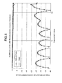
- FIG. 5 depicts propagation characteristics of the surface-layer signal line 21 in the high frequency module shown in FIGS. 1 to 3 , where ⁇ indicates reflection characteristics and 0 indicates pass characteristics.
- the multiplying and amplifying circuit 12 receives the signal of the frequency f0 outputted from the amplifying circuit 11 through the surface-layer signal line 21, multiplies the received signal by N, and amplifies the multiplied signal. Therefore, the surface-layer signal line 21 needs to have satisfactory pass characteristics at least for the signal of the frequency f0. As shown in FIG. 5 , satisfactory pass characteristics in each frequency band are obtained as the propagation characteristics of the surface-layer signal line 21.
- the high frequency storing case according to the present embodiment includes the waveguide aperture 30 and the end-short-circuited dielectric waveguide 40, and the waveguide aperture 30 and the end-short-circuited dielectric waveguide 40 are caused to operate as a reflection circuit for the signals that propagates within the cavity. Therefore, spatial isolation between the high frequency circuits can be ensured by an inexpensive and simple configuration using a single cavity, without using the expensive seal ring or cover member and feedthrough.
- the high frequency module of the present embodiment when a reference chip and a multiplication chip are separately laid out across the reflection circuit including the waveguide aperture 30 and the end-short-circuited dielectric waveguide 40, isolation between the chips can be ensured. Therefore, spatial feedback of a transmission wave (a multiplied wave) to the reference chip can be suppressed. That is, stable operations of the oscillator and the like, not affected by spatial loads can be expected because a reference wave thereof is cut off and a multiplied wave thereof is blocked by the reflection circuit.
- the oscillating circuit and the multiplying circuit are adopted as the high frequency circuits that are stored in the signal cavity 5.
- operation frequencies of the high frequency circuits are not limited to those of factors of a natural number, and first and second high frequency circuits having different operation frequency bands can be separately arranged across the reflection circuit including the waveguide aperture 30 and the end-short-circuited dielectric waveguide 40.
- the present invention is applied to the high frequency module having the high frequency circuits that are housed within the IC mounting recesses 6 formed in the multilayer dielectric substrate 2.
- the present invention can be also applied to a high frequency module having the high frequency circuits that are mounted on a flat surface layer of the multilayer dielectric substrate 2 having no IC mounting recesses 6.
- the cavity 5 can be formed by an earth conductor that is formed on the surface layer of the multilayer dielectric substrate 2 and on which the high frequency circuits are mounted, and the shield cover member 3.
- the high frequency storing case according to the present embodiment is effective in ensuring isolation between stages of a multistage amplifier chip in which there is a problem of spatial feedback due to tandem connection. That is, in such case, two or more amplifying circuits that operate in the same frequency band are separately arranged in the single cavity 5 across the reflection circuit including the waveguide aperture 30 and the end-short-circuited dielectric waveguide 40, respectively. This enables to easily ensure isolation between the respective amplifying circuits in which there is the problem of spatial feedback due to tandem connection, and prevention of oscillation can be expected.
- the high frequency storing case and the high frequency module according to the present invention are useful in cases where plural high frequency circuits that operate in different frequency bands are mounted.
Landscapes
- Microwave Amplifiers (AREA)
- Waveguides (AREA)
Applications Claiming Priority (2)
| Application Number | Priority Date | Filing Date | Title |
|---|---|---|---|
| JP2008124919 | 2008-05-12 | ||
| PCT/JP2009/053593 WO2009139210A1 (fr) | 2008-05-12 | 2009-02-26 | Boîtier de stockage haute fréquence et module haute fréquence |
Publications (3)
| Publication Number | Publication Date |
|---|---|
| EP2284881A1 true EP2284881A1 (fr) | 2011-02-16 |
| EP2284881A4 EP2284881A4 (fr) | 2014-08-27 |
| EP2284881B1 EP2284881B1 (fr) | 2021-02-17 |
Family
ID=41318583
Family Applications (1)
| Application Number | Title | Priority Date | Filing Date |
|---|---|---|---|
| EP09746417.6A Active EP2284881B1 (fr) | 2008-05-12 | 2009-02-26 | Module haute fréquence avec un boîtier et plusieurs circuits haute fréquence |
Country Status (5)
| Country | Link |
|---|---|
| US (1) | US8035994B2 (fr) |
| EP (1) | EP2284881B1 (fr) |
| JP (1) | JP5047357B2 (fr) |
| CN (1) | CN102027590B (fr) |
| WO (1) | WO2009139210A1 (fr) |
Families Citing this family (9)
| Publication number | Priority date | Publication date | Assignee | Title |
|---|---|---|---|---|
| KR20150075347A (ko) * | 2013-12-25 | 2015-07-03 | 가부시끼가이샤 도시바 | 반도체 패키지, 반도체 모듈 및 반도체 디바이스 |
| JP2015149649A (ja) | 2014-02-07 | 2015-08-20 | 株式会社東芝 | ミリ波帯用半導体パッケージおよびミリ波帯用半導体装置 |
| JP2015149650A (ja) | 2014-02-07 | 2015-08-20 | 株式会社東芝 | ミリ波帯用半導体パッケージおよびミリ波帯用半導体装置 |
| JP6400108B2 (ja) * | 2014-08-26 | 2018-10-03 | 三菱電機株式会社 | 高周波モジュール |
| CN104767010B (zh) * | 2015-04-03 | 2019-01-22 | 京信通信技术(广州)有限公司 | 一体式微波通信器件及天线 |
| US10375865B2 (en) * | 2017-03-24 | 2019-08-06 | Microsoft Technology Licensing, Llc | Mechanically attached edge shield |
| CN111092073B (zh) * | 2020-01-09 | 2025-06-27 | 芯思杰技术(深圳)股份有限公司 | 光电器件、芯片和芯片制作方法 |
| CN112259532B (zh) * | 2020-09-30 | 2022-12-13 | 中国电子科技集团公司第十三研究所 | 微波毫米波封装器件及其制作方法 |
| CN115996535B (zh) * | 2023-03-23 | 2023-08-08 | 成都雷电微力科技股份有限公司 | 一种Ka频段功放架构 |
Family Cites Families (22)
| Publication number | Priority date | Publication date | Assignee | Title |
|---|---|---|---|---|
| US3863181A (en) * | 1973-12-03 | 1975-01-28 | Bell Telephone Labor Inc | Mode suppressor for strip transmission lines |
| JPH064384B2 (ja) | 1987-08-04 | 1994-01-19 | 株式会社クボタ | トラクタのエンジン冷却構造 |
| JP3638173B2 (ja) * | 1996-03-27 | 2005-04-13 | 本田技研工業株式会社 | マイクロ波回路用パッケージ |
| US5668408A (en) | 1996-04-12 | 1997-09-16 | Hewlett-Packard Company | Pin grid array solution for microwave multi-chip modules |
| EP0874415B1 (fr) * | 1997-04-25 | 2006-08-23 | Kyocera Corporation | Module à haute fréquence |
| TW473882B (en) * | 1998-07-06 | 2002-01-21 | Hitachi Ltd | Semiconductor device |
| JP3538045B2 (ja) * | 1998-12-09 | 2004-06-14 | 三菱電機株式会社 | Rf回路モジュール |
| US6642808B2 (en) * | 2000-05-30 | 2003-11-04 | Kyocera Corporation | High frequency package, wiring board, and high frequency module having a cyclically varying transmission characteristic |
| JP2001352206A (ja) * | 2000-06-07 | 2001-12-21 | Mitsubishi Electric Corp | 高周波回路装置 |
| JP3570359B2 (ja) * | 2000-08-24 | 2004-09-29 | 三菱電機株式会社 | 高周波モジュール |
| JP2002164465A (ja) * | 2000-11-28 | 2002-06-07 | Kyocera Corp | 配線基板、配線ボード、それらの実装構造、ならびにマルチチップモジュール |
| JP4042338B2 (ja) * | 2001-03-30 | 2008-02-06 | 日本電気株式会社 | フリップチップ実装用基板 |
| KR100896405B1 (ko) * | 2001-12-14 | 2009-05-08 | 레어드 테크놀로지스 인코포레이티드 | 손실성 매체를 포함하는 emi 쉴딩 |
| US7276987B2 (en) * | 2002-10-29 | 2007-10-02 | Kyocera Corporation | High frequency line-to-waveguide converter and high frequency package |
| FR2847723B1 (fr) * | 2002-11-22 | 2006-02-03 | United Monolithic Semiconduct | Composant electronique en boitier pour applications a des frequences millimetriques |
| JP2004327641A (ja) * | 2003-04-24 | 2004-11-18 | Tdk Corp | 電子部品モジュール |
| US7336221B2 (en) * | 2004-03-26 | 2008-02-26 | Mitsubishi Denki Kabushiki Kaisha | High frequency package, transmitting and receiving module and wireless equipment |
| JP4634836B2 (ja) | 2004-03-26 | 2011-02-16 | 三菱電機株式会社 | 高周波パッケージ、送受信モジュールおよび無線装置 |
| JP4056500B2 (ja) * | 2004-06-28 | 2008-03-05 | 三菱電機株式会社 | 伝送線路基板および半導体パッケージ |
| JP2006253953A (ja) * | 2005-03-09 | 2006-09-21 | Fujitsu Ltd | 通信用高周波モジュールおよびその製造方法 |
| JP4575261B2 (ja) * | 2005-09-14 | 2010-11-04 | 株式会社東芝 | 高周波用パッケージ |
| KR100817070B1 (ko) * | 2006-10-30 | 2008-03-26 | 삼성전자주식회사 | 다중 그라운드 쉴딩 반도체 패키지, 그 패키지의 제조방법 및 그 그라운드 쉴딩을 이용한 노이즈 방지방법 |
-
2009
- 2009-02-26 EP EP09746417.6A patent/EP2284881B1/fr active Active
- 2009-02-26 US US12/918,239 patent/US8035994B2/en active Active
- 2009-02-26 JP JP2010511912A patent/JP5047357B2/ja active Active
- 2009-02-26 WO PCT/JP2009/053593 patent/WO2009139210A1/fr not_active Ceased
- 2009-02-26 CN CN2009801183562A patent/CN102027590B/zh active Active
Also Published As
| Publication number | Publication date |
|---|---|
| JPWO2009139210A1 (ja) | 2011-09-15 |
| JP5047357B2 (ja) | 2012-10-10 |
| WO2009139210A1 (fr) | 2009-11-19 |
| CN102027590A (zh) | 2011-04-20 |
| US8035994B2 (en) | 2011-10-11 |
| EP2284881A4 (fr) | 2014-08-27 |
| CN102027590B (zh) | 2013-09-25 |
| EP2284881B1 (fr) | 2021-02-17 |
| US20100315799A1 (en) | 2010-12-16 |
Similar Documents
| Publication | Publication Date | Title |
|---|---|---|
| EP2284881B1 (fr) | Module haute fréquence avec un boîtier et plusieurs circuits haute fréquence | |
| JP4188373B2 (ja) | 多層誘電体基板および半導体パッケージ | |
| EP1777775B1 (fr) | Substrat de ligne de transmission et boîtier de semiconducteur | |
| JP5960886B2 (ja) | 高周波回路パッケージおよびセンサモジュール | |
| US6657523B2 (en) | Stacked radio-frequency module | |
| JP5765174B2 (ja) | 電子装置 | |
| US10396025B2 (en) | Semiconductor device and amplifier apparatus | |
| EP2256800A1 (fr) | Substrat diélectrique multicouche et boîtier de semi-conducteur | |
| US20200259234A1 (en) | High frequency filter | |
| JP4634836B2 (ja) | 高周波パッケージ、送受信モジュールおよび無線装置 | |
| JP4516101B2 (ja) | 伝送線路基板および半導体パッケージ | |
| JP5334686B2 (ja) | 多層高周波パッケージ基板 | |
| JP3813946B2 (ja) | 高周波モジュール用ボード | |
| JP2023136491A (ja) | 平面線路・導波管変換器 | |
| JP2000133735A (ja) | 高周波集積回路用外囲器 | |
| JP2017045831A (ja) | 高周波パッケージ、送受信モジュール、およびレーダ装置 |
Legal Events
| Date | Code | Title | Description |
|---|---|---|---|
| PUAI | Public reference made under article 153(3) epc to a published international application that has entered the european phase |
Free format text: ORIGINAL CODE: 0009012 |
|
| 17P | Request for examination filed |
Effective date: 20101116 |
|
| AK | Designated contracting states |
Kind code of ref document: A1 Designated state(s): AT BE BG CH CY CZ DE DK EE ES FI FR GB GR HR HU IE IS IT LI LT LU LV MC MK MT NL NO PL PT RO SE SI SK TR |
|
| AX | Request for extension of the european patent |
Extension state: AL BA RS |
|
| DAX | Request for extension of the european patent (deleted) | ||
| A4 | Supplementary search report drawn up and despatched |
Effective date: 20140728 |
|
| RIC1 | Information provided on ipc code assigned before grant |
Ipc: H01L 25/18 20060101ALI20140722BHEP Ipc: H01L 23/66 20060101ALI20140722BHEP Ipc: H01L 23/552 20060101ALI20140722BHEP Ipc: G01S 7/02 20060101ALI20140722BHEP Ipc: H01L 23/12 20060101ALI20140722BHEP Ipc: H01L 23/02 20060101AFI20140722BHEP Ipc: H01L 25/04 20140101ALI20140722BHEP |
|
| STAA | Information on the status of an ep patent application or granted ep patent |
Free format text: STATUS: EXAMINATION IS IN PROGRESS |
|
| 17Q | First examination report despatched |
Effective date: 20180525 |
|
| GRAP | Despatch of communication of intention to grant a patent |
Free format text: ORIGINAL CODE: EPIDOSNIGR1 |
|
| STAA | Information on the status of an ep patent application or granted ep patent |
Free format text: STATUS: GRANT OF PATENT IS INTENDED |
|
| RIC1 | Information provided on ipc code assigned before grant |
Ipc: H05K 9/00 20060101ALI20190325BHEP Ipc: G01S 7/02 20060101ALN20190325BHEP Ipc: H01L 23/552 20060101ALI20190325BHEP Ipc: H01P 3/12 20060101ALI20190325BHEP Ipc: H01L 23/043 20060101AFI20190325BHEP Ipc: H01P 5/107 20060101ALN20190325BHEP Ipc: H05K 7/00 20060101ALI20190325BHEP Ipc: H01L 23/66 20060101ALI20190325BHEP Ipc: H01P 3/16 20060101ALN20190325BHEP |
|
| RIC1 | Information provided on ipc code assigned before grant |
Ipc: H01P 3/12 20060101ALI20190410BHEP Ipc: H01L 23/043 20060101AFI20190410BHEP Ipc: H01L 23/552 20060101ALI20190410BHEP Ipc: H05K 7/00 20060101ALI20190410BHEP Ipc: H01P 3/16 20060101ALN20190410BHEP Ipc: H01P 5/107 20060101ALN20190410BHEP Ipc: G01S 7/02 20060101ALN20190410BHEP Ipc: H01L 23/66 20060101ALI20190410BHEP Ipc: H05K 9/00 20060101ALI20190410BHEP |
|
| INTG | Intention to grant announced |
Effective date: 20190429 |
|
| GRAJ | Information related to disapproval of communication of intention to grant by the applicant or resumption of examination proceedings by the epo deleted |
Free format text: ORIGINAL CODE: EPIDOSDIGR1 |
|
| STAA | Information on the status of an ep patent application or granted ep patent |
Free format text: STATUS: EXAMINATION IS IN PROGRESS |
|
| INTC | Intention to grant announced (deleted) | ||
| REG | Reference to a national code |
Ref country code: DE Ref legal event code: R079 Ref document number: 602009063336 Country of ref document: DE Free format text: PREVIOUS MAIN CLASS: H01L0023020000 Ipc: H01L0023043000 |
|
| GRAP | Despatch of communication of intention to grant a patent |
Free format text: ORIGINAL CODE: EPIDOSNIGR1 |
|
| STAA | Information on the status of an ep patent application or granted ep patent |
Free format text: STATUS: GRANT OF PATENT IS INTENDED |
|
| RIC1 | Information provided on ipc code assigned before grant |
Ipc: H01L 23/66 20060101ALI20200818BHEP Ipc: H05K 7/00 20060101ALI20200818BHEP Ipc: G01S 7/02 20060101ALN20200818BHEP Ipc: H01P 3/16 20060101ALN20200818BHEP Ipc: H01P 5/107 20060101ALN20200818BHEP Ipc: H01L 23/043 20060101AFI20200818BHEP Ipc: H01P 3/12 20060101ALI20200818BHEP Ipc: H05K 9/00 20060101ALI20200818BHEP Ipc: H01L 23/552 20060101ALI20200818BHEP |
|
| INTG | Intention to grant announced |
Effective date: 20200831 |
|
| GRAS | Grant fee paid |
Free format text: ORIGINAL CODE: EPIDOSNIGR3 |
|
| GRAA | (expected) grant |
Free format text: ORIGINAL CODE: 0009210 |
|
| STAA | Information on the status of an ep patent application or granted ep patent |
Free format text: STATUS: THE PATENT HAS BEEN GRANTED |
|
| AK | Designated contracting states |
Kind code of ref document: B1 Designated state(s): AT BE BG CH CY CZ DE DK EE ES FI FR GB GR HR HU IE IS IT LI LT LU LV MC MK MT NL NO PL PT RO SE SI SK TR |
|
| REG | Reference to a national code |
Ref country code: GB Ref legal event code: FG4D |
|
| REG | Reference to a national code |
Ref country code: CH Ref legal event code: EP |
|
| REG | Reference to a national code |
Ref country code: DE Ref legal event code: R096 Ref document number: 602009063336 Country of ref document: DE |
|
| REG | Reference to a national code |
Ref country code: AT Ref legal event code: REF Ref document number: 1362586 Country of ref document: AT Kind code of ref document: T Effective date: 20210315 |
|
| REG | Reference to a national code |
Ref country code: IE Ref legal event code: FG4D |
|
| REG | Reference to a national code |
Ref country code: LT Ref legal event code: MG9D |
|
| REG | Reference to a national code |
Ref country code: NL Ref legal event code: MP Effective date: 20210217 |
|
| PG25 | Lapsed in a contracting state [announced via postgrant information from national office to epo] |
Ref country code: BG Free format text: LAPSE BECAUSE OF FAILURE TO SUBMIT A TRANSLATION OF THE DESCRIPTION OR TO PAY THE FEE WITHIN THE PRESCRIBED TIME-LIMIT Effective date: 20210517 Ref country code: NO Free format text: LAPSE BECAUSE OF FAILURE TO SUBMIT A TRANSLATION OF THE DESCRIPTION OR TO PAY THE FEE WITHIN THE PRESCRIBED TIME-LIMIT Effective date: 20210517 Ref country code: PT Free format text: LAPSE BECAUSE OF FAILURE TO SUBMIT A TRANSLATION OF THE DESCRIPTION OR TO PAY THE FEE WITHIN THE PRESCRIBED TIME-LIMIT Effective date: 20210617 Ref country code: GR Free format text: LAPSE BECAUSE OF FAILURE TO SUBMIT A TRANSLATION OF THE DESCRIPTION OR TO PAY THE FEE WITHIN THE PRESCRIBED TIME-LIMIT Effective date: 20210518 Ref country code: FI Free format text: LAPSE BECAUSE OF FAILURE TO SUBMIT A TRANSLATION OF THE DESCRIPTION OR TO PAY THE FEE WITHIN THE PRESCRIBED TIME-LIMIT Effective date: 20210217 Ref country code: HR Free format text: LAPSE BECAUSE OF FAILURE TO SUBMIT A TRANSLATION OF THE DESCRIPTION OR TO PAY THE FEE WITHIN THE PRESCRIBED TIME-LIMIT Effective date: 20210217 Ref country code: LT Free format text: LAPSE BECAUSE OF FAILURE TO SUBMIT A TRANSLATION OF THE DESCRIPTION OR TO PAY THE FEE WITHIN THE PRESCRIBED TIME-LIMIT Effective date: 20210217 |
|
| REG | Reference to a national code |
Ref country code: AT Ref legal event code: MK05 Ref document number: 1362586 Country of ref document: AT Kind code of ref document: T Effective date: 20210217 |
|
| PG25 | Lapsed in a contracting state [announced via postgrant information from national office to epo] |
Ref country code: SE Free format text: LAPSE BECAUSE OF FAILURE TO SUBMIT A TRANSLATION OF THE DESCRIPTION OR TO PAY THE FEE WITHIN THE PRESCRIBED TIME-LIMIT Effective date: 20210217 Ref country code: PL Free format text: LAPSE BECAUSE OF FAILURE TO SUBMIT A TRANSLATION OF THE DESCRIPTION OR TO PAY THE FEE WITHIN THE PRESCRIBED TIME-LIMIT Effective date: 20210217 Ref country code: LV Free format text: LAPSE BECAUSE OF FAILURE TO SUBMIT A TRANSLATION OF THE DESCRIPTION OR TO PAY THE FEE WITHIN THE PRESCRIBED TIME-LIMIT Effective date: 20210217 Ref country code: NL Free format text: LAPSE BECAUSE OF FAILURE TO SUBMIT A TRANSLATION OF THE DESCRIPTION OR TO PAY THE FEE WITHIN THE PRESCRIBED TIME-LIMIT Effective date: 20210217 |
|
| PG25 | Lapsed in a contracting state [announced via postgrant information from national office to epo] |
Ref country code: IS Free format text: LAPSE BECAUSE OF FAILURE TO SUBMIT A TRANSLATION OF THE DESCRIPTION OR TO PAY THE FEE WITHIN THE PRESCRIBED TIME-LIMIT Effective date: 20210617 |
|
| REG | Reference to a national code |
Ref country code: BE Ref legal event code: MM Effective date: 20210228 |
|
| PG25 | Lapsed in a contracting state [announced via postgrant information from national office to epo] |
Ref country code: LU Free format text: LAPSE BECAUSE OF NON-PAYMENT OF DUE FEES Effective date: 20210226 Ref country code: LI Free format text: LAPSE BECAUSE OF NON-PAYMENT OF DUE FEES Effective date: 20210228 Ref country code: EE Free format text: LAPSE BECAUSE OF FAILURE TO SUBMIT A TRANSLATION OF THE DESCRIPTION OR TO PAY THE FEE WITHIN THE PRESCRIBED TIME-LIMIT Effective date: 20210217 Ref country code: CZ Free format text: LAPSE BECAUSE OF FAILURE TO SUBMIT A TRANSLATION OF THE DESCRIPTION OR TO PAY THE FEE WITHIN THE PRESCRIBED TIME-LIMIT Effective date: 20210217 Ref country code: AT Free format text: LAPSE BECAUSE OF FAILURE TO SUBMIT A TRANSLATION OF THE DESCRIPTION OR TO PAY THE FEE WITHIN THE PRESCRIBED TIME-LIMIT Effective date: 20210217 Ref country code: CH Free format text: LAPSE BECAUSE OF NON-PAYMENT OF DUE FEES Effective date: 20210228 |
|
| REG | Reference to a national code |
Ref country code: DE Ref legal event code: R097 Ref document number: 602009063336 Country of ref document: DE |
|
| PG25 | Lapsed in a contracting state [announced via postgrant information from national office to epo] |
Ref country code: RO Free format text: LAPSE BECAUSE OF FAILURE TO SUBMIT A TRANSLATION OF THE DESCRIPTION OR TO PAY THE FEE WITHIN THE PRESCRIBED TIME-LIMIT Effective date: 20210217 Ref country code: SK Free format text: LAPSE BECAUSE OF FAILURE TO SUBMIT A TRANSLATION OF THE DESCRIPTION OR TO PAY THE FEE WITHIN THE PRESCRIBED TIME-LIMIT Effective date: 20210217 Ref country code: MC Free format text: LAPSE BECAUSE OF FAILURE TO SUBMIT A TRANSLATION OF THE DESCRIPTION OR TO PAY THE FEE WITHIN THE PRESCRIBED TIME-LIMIT Effective date: 20210217 Ref country code: DK Free format text: LAPSE BECAUSE OF FAILURE TO SUBMIT A TRANSLATION OF THE DESCRIPTION OR TO PAY THE FEE WITHIN THE PRESCRIBED TIME-LIMIT Effective date: 20210217 Ref country code: ES Free format text: LAPSE BECAUSE OF FAILURE TO SUBMIT A TRANSLATION OF THE DESCRIPTION OR TO PAY THE FEE WITHIN THE PRESCRIBED TIME-LIMIT Effective date: 20210217 |
|
| PLBE | No opposition filed within time limit |
Free format text: ORIGINAL CODE: 0009261 |
|
| STAA | Information on the status of an ep patent application or granted ep patent |
Free format text: STATUS: NO OPPOSITION FILED WITHIN TIME LIMIT |
|
| 26N | No opposition filed |
Effective date: 20211118 |
|
| GBPC | Gb: european patent ceased through non-payment of renewal fee |
Effective date: 20210517 |
|
| PG25 | Lapsed in a contracting state [announced via postgrant information from national office to epo] |
Ref country code: FR Free format text: LAPSE BECAUSE OF NON-PAYMENT OF DUE FEES Effective date: 20210417 Ref country code: IE Free format text: LAPSE BECAUSE OF NON-PAYMENT OF DUE FEES Effective date: 20210226 |
|
| PG25 | Lapsed in a contracting state [announced via postgrant information from national office to epo] |
Ref country code: SI Free format text: LAPSE BECAUSE OF FAILURE TO SUBMIT A TRANSLATION OF THE DESCRIPTION OR TO PAY THE FEE WITHIN THE PRESCRIBED TIME-LIMIT Effective date: 20210217 |
|
| PG25 | Lapsed in a contracting state [announced via postgrant information from national office to epo] |
Ref country code: IT Free format text: LAPSE BECAUSE OF FAILURE TO SUBMIT A TRANSLATION OF THE DESCRIPTION OR TO PAY THE FEE WITHIN THE PRESCRIBED TIME-LIMIT Effective date: 20210217 Ref country code: GB Free format text: LAPSE BECAUSE OF NON-PAYMENT OF DUE FEES Effective date: 20210517 |
|
| PG25 | Lapsed in a contracting state [announced via postgrant information from national office to epo] |
Ref country code: IS Free format text: LAPSE BECAUSE OF FAILURE TO SUBMIT A TRANSLATION OF THE DESCRIPTION OR TO PAY THE FEE WITHIN THE PRESCRIBED TIME-LIMIT Effective date: 20210617 |
|
| PG25 | Lapsed in a contracting state [announced via postgrant information from national office to epo] |
Ref country code: BE Free format text: LAPSE BECAUSE OF NON-PAYMENT OF DUE FEES Effective date: 20210228 |
|
| PG25 | Lapsed in a contracting state [announced via postgrant information from national office to epo] |
Ref country code: CY Free format text: LAPSE BECAUSE OF FAILURE TO SUBMIT A TRANSLATION OF THE DESCRIPTION OR TO PAY THE FEE WITHIN THE PRESCRIBED TIME-LIMIT Effective date: 20210217 Ref country code: HU Free format text: LAPSE BECAUSE OF FAILURE TO SUBMIT A TRANSLATION OF THE DESCRIPTION OR TO PAY THE FEE WITHIN THE PRESCRIBED TIME-LIMIT; INVALID AB INITIO Effective date: 20090226 |
|
| P01 | Opt-out of the competence of the unified patent court (upc) registered |
Effective date: 20230512 |
|
| REG | Reference to a national code |
Ref country code: DE Ref legal event code: R084 Ref document number: 602009063336 Country of ref document: DE |
|
| PG25 | Lapsed in a contracting state [announced via postgrant information from national office to epo] |
Ref country code: MK Free format text: LAPSE BECAUSE OF FAILURE TO SUBMIT A TRANSLATION OF THE DESCRIPTION OR TO PAY THE FEE WITHIN THE PRESCRIBED TIME-LIMIT Effective date: 20210217 |
|
| PG25 | Lapsed in a contracting state [announced via postgrant information from national office to epo] |
Ref country code: TR Free format text: LAPSE BECAUSE OF FAILURE TO SUBMIT A TRANSLATION OF THE DESCRIPTION OR TO PAY THE FEE WITHIN THE PRESCRIBED TIME-LIMIT Effective date: 20210217 |
|
| PG25 | Lapsed in a contracting state [announced via postgrant information from national office to epo] |
Ref country code: MT Free format text: LAPSE BECAUSE OF FAILURE TO SUBMIT A TRANSLATION OF THE DESCRIPTION OR TO PAY THE FEE WITHIN THE PRESCRIBED TIME-LIMIT Effective date: 20210217 |
|
| REG | Reference to a national code |
Ref country code: DE Ref legal event code: R079 Ref document number: 602009063336 Country of ref document: DE Free format text: PREVIOUS MAIN CLASS: H01L0023043000 Ipc: H10W0076130000 |
|
| PGFP | Annual fee paid to national office [announced via postgrant information from national office to epo] |
Ref country code: DE Payment date: 20260102 Year of fee payment: 18 |