EP2287596B1 - Sensor mit Glob-Top und Herstellungsverfahren dafür - Google Patents
Sensor mit Glob-Top und Herstellungsverfahren dafür Download PDFInfo
- Publication number
- EP2287596B1 EP2287596B1 EP09010327.6A EP09010327A EP2287596B1 EP 2287596 B1 EP2287596 B1 EP 2287596B1 EP 09010327 A EP09010327 A EP 09010327A EP 2287596 B1 EP2287596 B1 EP 2287596B1
- Authority
- EP
- European Patent Office
- Prior art keywords
- auxiliary layer
- sensor
- glob
- substrate
- section
- Prior art date
- Legal status (The legal status is an assumption and is not a legal conclusion. Google has not performed a legal analysis and makes no representation as to the accuracy of the status listed.)
- Active
Links
Images
Classifications
-
- G—PHYSICS
- G01—MEASURING; TESTING
- G01N—INVESTIGATING OR ANALYSING MATERIALS BY DETERMINING THEIR CHEMICAL OR PHYSICAL PROPERTIES
- G01N27/00—Investigating or analysing materials by the use of electric, electrochemical, or magnetic means
- G01N27/02—Investigating or analysing materials by the use of electric, electrochemical, or magnetic means by investigating impedance
- G01N27/04—Investigating or analysing materials by the use of electric, electrochemical, or magnetic means by investigating impedance by investigating resistance
- G01N27/12—Investigating or analysing materials by the use of electric, electrochemical, or magnetic means by investigating impedance by investigating resistance of a solid body in dependence upon absorption of a fluid; of a solid body in dependence upon reaction with a fluid, for detecting components in the fluid
- G01N27/128—Microapparatus
-
- G—PHYSICS
- G01—MEASURING; TESTING
- G01N—INVESTIGATING OR ANALYSING MATERIALS BY DETERMINING THEIR CHEMICAL OR PHYSICAL PROPERTIES
- G01N27/00—Investigating or analysing materials by the use of electric, electrochemical, or magnetic means
- G01N27/02—Investigating or analysing materials by the use of electric, electrochemical, or magnetic means by investigating impedance
- G01N27/04—Investigating or analysing materials by the use of electric, electrochemical, or magnetic means by investigating impedance by investigating resistance
- G01N27/12—Investigating or analysing materials by the use of electric, electrochemical, or magnetic means by investigating impedance by investigating resistance of a solid body in dependence upon absorption of a fluid; of a solid body in dependence upon reaction with a fluid, for detecting components in the fluid
- G01N27/121—Investigating or analysing materials by the use of electric, electrochemical, or magnetic means by investigating impedance by investigating resistance of a solid body in dependence upon absorption of a fluid; of a solid body in dependence upon reaction with a fluid, for detecting components in the fluid for determining moisture content, e.g. humidity, of the fluid
-
- G—PHYSICS
- G01—MEASURING; TESTING
- G01N—INVESTIGATING OR ANALYSING MATERIALS BY DETERMINING THEIR CHEMICAL OR PHYSICAL PROPERTIES
- G01N27/00—Investigating or analysing materials by the use of electric, electrochemical, or magnetic means
- G01N27/02—Investigating or analysing materials by the use of electric, electrochemical, or magnetic means by investigating impedance
- G01N27/22—Investigating or analysing materials by the use of electric, electrochemical, or magnetic means by investigating impedance by investigating capacitance
- G01N27/223—Investigating or analysing materials by the use of electric, electrochemical, or magnetic means by investigating impedance by investigating capacitance for determining moisture content, e.g. humidity
-
- H—ELECTRICITY
- H10—SEMICONDUCTOR DEVICES; ELECTRIC SOLID-STATE DEVICES NOT OTHERWISE PROVIDED FOR
- H10W—GENERIC PACKAGES, INTERCONNECTIONS, CONNECTORS OR OTHER CONSTRUCTIONAL DETAILS OF DEVICES COVERED BY CLASS H10
- H10W74/00—Encapsulations, e.g. protective coatings
- H10W74/10—Encapsulations, e.g. protective coatings characterised by their shape or disposition
- H10W74/131—Encapsulations, e.g. protective coatings characterised by their shape or disposition the semiconductor body being only partially enclosed
Definitions
- the invention relates to a sensor having a substrate, which is covered in part by a glob of hardened material, and to a method for manufacturing such a sensor.
- Integrated sensors typically comprise a substrate, such as a semiconductor chip, with a sensor device arranged on a surface thereof.
- a substrate such as a semiconductor chip
- Such sensors can e.g. be "packaged” using the so-called “glob-top” technology, where a glob or drop of resin is placed on the surface of the substrate and covers the bond wires.
- the glob protects the bond wires and substrate and also provides or improves the mechanical connection between the substrate and an underlying support, such as a printed circuit board.
- the sensor comprises a sensor device that needs to be in contact with the environment, e.g. if the sensor device is a humidity sensor or a substance sensor, applying the glob becomes difficult since the glob must not cover the sensor device.
- US 2005/031490 A1 discloses an analysis device that may be used in biochemical analyses which device includes a module in a first housing, including a chip support, a sensor chip and electrical contacts between the chip and the chip support.
- the chip is encapsulated so that the electrical contacts are insulated and the sensitive surface of the sensor chip remains accessible to a fluid to be tested.
- a polyimide ring 27 in form of a dam serves as delimitation of the sensitive surface with respect to the encapsulation.
- US 6,566,745 Bl is related to an image sensor packaging technique based on a Ball Grid Array (BGA) IC packaging technique, further referred to as image sensor ball grid array (ISBGA).
- BGA Ball Grid Array
- ISBGA image sensor ball grid array
- a transparent cover is attached to a semiconductor substrate.
- a hermetic or non-hermitic sealing is obtained.
- the obtained structure can be connected trough wire-bonding or flip chip connection. Deposition of a dam prevents the optical sensing area from being covered with polymeric sealant during a glob top deposition.
- a package for a microelectronic component comprising a carrier element having a first side that comprises conductor lines, a microelectronic component having a first surface and a second surface facing away from the first surface, the microelectronic component with said second surface being mounted on said first side of said carrier element and connected to the conductor lines via bonding wires, a polymeric encapsulation material encapsulating the bonding wires and exposing a central zone of said first surface of said microelectronic component, the encapsulation material comprising an outer edge at said first side of the carrier element and an inner edge at said first surface of said microelectronic component, a dam on the carrier device abutting to the encapsulation material.
- the dam influences the forming of the outer and the inner edge during manufacturing the encapsulation material and enlarges the area of the central zone.
- WO 01/40784 A2 relates to a sensor for measuring the parameters of a fluid, in particular, for detecting the presence of substances contained in a gas.
- the sensor comprises a measuring device that is placed on a semiconductor chip which is protected by a housing.
- a partition of the housing divides the semiconductor chip into two parts. The first part is connected to the exterior via openings in the housing and carries the measureing device. The second part is covered by a hardened sealing material.
- the sealing material protects the semiconductor chip from undesirable environmental influences.
- the partition forms a capillary between the chip and the housing, the capillary action thereof draws in the sealing material, and the end thereof stops the sealing material.
- the problem to be solved by the present invention is therefore to provide a method and a sensor that make it easier to use glob-top technology for sensors that need to be in contact with their environment.
- an auxiliary layer is arranged on the substrate and structured to form at least one edge, which edge extends along at least part of a (virtual) border dividing the first surface, i.e. the surface into which the sensor device has been integrated, into a first and a second section.
- the sensor device is at least partially arranged in the first section.
- a glob of hardening material such as a hardening resin, is applied to at least part of the second section and the edge is used as a stop for preventing the glob from entering the first section.
- the edge is used as a stop for preventing the glob from entering the first section.
- the sensor manufactured in this way will comprise: a substrate with the sensor device integrated on its first side; the structured auxiliary layer arranged on the first side and having said edge extending along the border dividing the first and second sections of the surface; and the glob of hardened material covering at least part of the second section, with an edge of the glob extending along the edge of the auxiliary layer.
- the auxiliary layer is structured photolithographically. It can e.g. be a photoresist because, on the one hand, structuring a photoresist is a well-known technique, and, on the other hand, resins, or, more generally, organic materials, have been found to be suited as a good stop for the glob material.
- the present invention is especially well suited for substance sensors, such as humidity sensors, whose sensor device must not be covered by the glob-top, but it e.g. can also be applied to optical sensors, flow sensors or other sensor types.
- the invention is well suited for being used with even very small sensor substrates as it exploits surface tension effects.
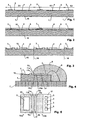
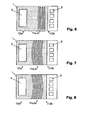
- FIG. 5 through 8 show the auxiliary layer with a dotted pattern.
- the sensor of Fig. 4 comprises a substrate 1, which is a semiconductor substrate.
- Substrate 1 has a first surface 2, namely its top surface in Fig. 4 .
- Substrate 1 carries a sensor device 3 on its surface 2.
- Sensor device 3 can e.g. be a moisture adsorbing film, such as a porous polymer, whose dielectric constant varies with environmental humidity.
- An arrangement of electrodes, such as a set of interdigital electrodes integrated below the film, allows to determine the humidity by means of a capacitive measurement.
- a device of this type is e.g. described in US 6690569 .
- substrate 1 can carry further elements in its surface 2, such as an integrated circuitry 4, which can e.g. comprise digital and/or analogue processing and/or control circuits. It must be noted, though, that the invention may also be carried out with devices not having any integrated circuitry.
- integrated circuitry 4 can e.g. comprise digital and/or analogue processing and/or control circuits. It must be noted, though, that the invention may also be carried out with devices not having any integrated circuitry.
- the sensor further comprises a set of contact pads 5, which are also integrated on surface 2, for electrically connecting the circuitry 4 and/or sensor device 3 to bond wires 6.
- the bond wires 6 can, in turn, be connected to electrical leads on a support 7, such as a printed circuit board.
- a glob 8 of hardening material is applied to first surface 2 as well as to support 7. It covers the bond wires 6.
- the sensor further comprises an auxiliary layer 10 applied to first surface 2.
- auxiliary layer 10 is structured to form one or more edges 11a, 11b, which traverse at least part of first surface 2. Each edge extends along at least part of a border or border line 11, as shown in Fig. 5 , which separates surface 2 into a first and a second section 12a, 12b, respectively.
- Sensor device 3 is located in part or completely in first section 12a, while glob 8 covers at least part of second section 12b.
- An edge 13 of glob 8 extends along at least part of one of the edges 11a or 11b.
- a wafer 15 which comprises a plurality of the substrates 1 that will later be cut from the wafer in order to form the individual sensors.
- the regions of three of the individual sensors are marked in Fig. 1 by S1, S2, and S3.
- Each substrate 1 on wafer 15 carries at least one of the sensor devices 3 on its first surface 2, and circuitry 4 as well as the bond pads 5 have also been applied thereto, e.g. using conventional CMOS manufacturing technology.
- auxiliary layer 10 covers each substrate 1 completely.
- auxiliary layer 10 is a photoresist, in particular SU-8.
- SU-8 photoresist
- Materials allowing structuring by means of photolithography are advantageous because photolithography is typically also used for creating the other structures on substrate 1, thus the structuring of auxiliary layer 10 can be integrated efficiently and accurately in the manufacturing process of the sensor.
- auxiliary layer 10 is structured on wafer 15.
- the purpose of the structuring process is to form the edges 11a, 11b mentioned above, as well as some additional structures.
- the edges 11a, 11b are created by removing a plurality of substantially parallel, strip-shaped regions 16 from auxiliary layer 10 (see Fig. 5 ).
- a region 17 at the location of the contact pads 5 and at least part of auxiliary layer 10 over sensor device 3 are removed.
- wafer 15 can be diced (cut) along lines 18 into the individual sensors S1, S2, S3, etc.
- each substrate 1 is placed on a support 7 and can e.g. be glued thereto, and bond wires 6 are attached to the bond pads 5 of substrate 1 as well as to the leads on support 7.
- glob 8 is (in liquid form) applied to the second region 12b of surface 2 as well as to the support 7 adjacent thereto, thereby covering the bond wires 6. While still in its liquid state, glob 8 will expand laterally and approach sensor device 3. However, as described above, its forward edge 13 will in most cases be stopped when reaching the first edge 11a of auxiliary layer 10. If it is not stopped there, it may expand further until it reaches a next edge of auxiliary layer 10, where the probability of the glob expansion to be stopped is even higher. Hence, if an appropriate amount of glob material is applied, the glob will be stopped at one of the edges 11a, 11b and not cover sensor device 3.
- glob 8 can be hardened.
- the material of glob 8 is advantageously a resin that is crosslinked after its application to substrate 1.
- the following material can be used: Hysol EO1062, Hysol FP4450 (Henkel); and Stycast 50300 (National Starch and Chemical Company).
- the expansion of glob 8 will either be stopped at a "negative edge" 11a or at a positive edge 11b of auxiliary layer 10. If, for example, a resin is used for glob 8 and SU-8 is used for auxiliary layer 10, while the surface 2 is of silicon oxide or silicon nitride, expansion generally stops at a negative edge 11a (i.e. at a transition from the auxiliary layer to the material of surface 2).
- auxiliary layer 10 should be an organic material, such as a resin or other polymer, while surface 2 is of an inorganic material, such as silicon nitride, silicon oxide or glass, or a mixture of such materials.
- auxiliary layer 10 it should be thick in order to create a high step at the edges 11a, 11b.
- the thickness is at least 5 ⁇ m, in particular at least 10 ⁇ m.
- the auxiliary layer 10 of the present invention acts as such a buffer structure and also forms a frame 20 around sensor device 3, thus making it possible to package the sensor either in the manner as shown in Fig. 4 of the present application, or in the manner as shown in Fig. 6 of WO 2006/114005 .
- forming a frame around the sensor device is to be understood such that the auxiliary layer, i.e. the buffer structure, extends continuously around an opening located above the sensor device.
- sensor device 3 is a flow sensor device, such as a thermal flow sensor device
- light sensors where sensor device 3 is an optical detector
Landscapes
- Chemical & Material Sciences (AREA)
- Chemical Kinetics & Catalysis (AREA)
- Electrochemistry (AREA)
- Physics & Mathematics (AREA)
- Health & Medical Sciences (AREA)
- Life Sciences & Earth Sciences (AREA)
- Analytical Chemistry (AREA)
- Biochemistry (AREA)
- General Health & Medical Sciences (AREA)
- General Physics & Mathematics (AREA)
- Immunology (AREA)
- Pathology (AREA)
- Solid State Image Pick-Up Elements (AREA)
- Investigating Or Analyzing Materials By The Use Of Electric Means (AREA)
Claims (16)
- Ein Verfahren zur Herstellung eines Sensors, umfassend die Schritte:- Bereitstellen eines Halbleitersubstrats (1) mit mindestens einer Sensorvorrichtung (3) auf einer ersten Oberfläche (2),- Bedecken des Substrats (1) mit einer Hilfsschicht (10),- Strukturieren der Hilfsschicht (10), indem ein Teil der Hilfsschicht (10) abgetragen wird, um mindestens eine Kante (11a, 11b) in der Hilfsschicht (10) zu bilden, wobei sich die Kante (11a, 11b) entlang mindestens eines Teils einer Grenze (11), die die erste Oberfläche (2) in einen ersten und in einen zweiten Bereich (12a, 12b) teilt, erstreckt, wobei die Sensorvorrichtung (3) mindestens teilweise im ersten Bereich (12a) angeordnet ist,- Auftragen eine Vergussmasse (8) eines Aushärtungsmaterials auf mindestens einen Teil des zweiten Bereichs (12b), wobei die Kante (11a, 11b) in der Form eines Übergangs von der Hilfsschicht (10) zu einem Material der Oberfläche (2) als eine Sperre verwendet wird, um zu verhindern, dass die Vergussmasse (8) in den ersten Bereich (12a) dringt, und- Härten der Vergussmasse (8).
- Das Verfahren nach Anspruch 1, wobei der Schritt der Strukturierung der Hilfsschicht (10) mit Fotolithographie ausgeführt wird.
- Das Verfahren nach einem der vorangehenden Ansprüche, wobei die Hilfsschicht (10) ein Polymer, insbesondere ein Harz, ist.
- Das Verfahren nach Anspruch 3, wobei die Schicht eine Fotolackschicht ist, insbesondere SU-8.
- Das Verfahren nach einem der vorangehenden Ansprüche, umfassend den Schritt der Bildung einer Vielzahl von Kanten (11a, 11b) der Hilfsschicht (10) auf dem Substrat (1), wobei die Kanten (11a, 11b) im Wesentlichen parallel sind.
- Das Verfahren nach Anspruch 5, wobei die Kanten (11a, 11b) durch Abtragung einer Vielzahl von streifenförmigen, im Wesentlichen parallelen Bereichen (16) der Hilfsschicht (10) gebildet werden.
- Das Verfahren nach einem der vorangehenden Ansprüche, weiter umfassend den Schritt der Abtragung mindestens eines Teils der Hilfsschicht (10), die die Sensorvorrichtung (3) bedeckt, während der Strukturierung der Hilfsschicht (10).
- Das Verfahren nach einem der vorangehenden Ansprüche, umfassend die Schritte- Bereitstellen einer Vielzahl von Substraten (1) als ein Wafer (15),- Bedecken des Substrats (1) mit der Hilfsschicht (10) durch Bedecken des Wafers (15),- Strukturieren der Hilfsschicht (10) auf dem Wafer (15), und- Vereinzeln des Wafers (15) in die einzelnen Substrate (1) nach der Strukturierung der Hilfsschicht (10).
- Das Verfahren nach einem der vorangehenden Ansprüche, weiter umfassend die Schritte der Befestigung von Bonddrähten (6) am Substrat (1) und Bedecken der Bonddrähte (6) mit der Vergussmasse (8).
- Das Verfahren nach einem der vorangehenden Ansprüche, wobei die erste Oberfläche (2) des Substrats (1) aus anorganischem Material gebildet ist, insbesondere aus einem Material umfassend mindestens ein Element der Gruppe: Siliziumnitrid, Siliziumoxid und Glas.
- Das Verfahren nach einem der vorangehenden Ansprüche, weiter umfassend die Schritte- Anordnen des Substrats (1) auf einem Träger (7) und- Aufbringen der Vergussmasse (8) auf die erste Oberfläche (2) sowie auf den Träger (7).
- Das Verfahren nach einem der vorangehenden Ansprüche, wobei eine Dicke der Hilfsschicht (10) mindestens 5 µm, insbesondere mindestens 10 µm, beträgt.
- Ein Sensor, insbesondere hergestellt mittels des Verfahrens nach einem der vorangehenden Ansprüche, umfassend
ein Halbleitersubstrat (1),
eine Sensorvorrichtung (3), die auf einer ersten Oberfläche (2) des Substrats (1) integriert ist,
eine strukturierte Hilfsschicht (10), die auf der ersten Oberfläche (2) angeordnet ist, wobei die Hilfsschicht (10) mindestens eine Kante (11a, 11b) umfasst, die sich entlang mindestens eines Teils einer Grenze (11) erstreckt, wobei die Grenze (11) die erste Oberfläche (2) in einen ersten und in einen zweiten Bereich (12a, 12b) teilt, wobei die Sensorvorrichtung (3) im ersten Bereich (12a) angeordnet ist, und
eine Vergussmasse (8) aus gehärtetem Material, die mindestens einen Teil des zweiten Bereichs (12b) bedeckt und die Hilfsschicht (10) im zweiten Bereich (12b) bedeckt, wobei sich eine Kante (13) der Vergussmasse (8) entlang der Kante (11a, 11b) der Hilfsschicht (10) erstreckt. - Der Sensor nach Anspruch 13, wobei die Hilfsschicht (10) eine strukturierte Fotolackschicht ist.
- Der Sensor einem der Ansprüche 13 oder 14, wobei der Sensor ein Feuchtigkeitssensor ist.
- Sensor nach einem der Ansprüche 13 bis 15, wobei die Hilfsschicht (10) einen Rahmen (20) um die Sensorvorrichtung (3) bildet.
Priority Applications (1)
| Application Number | Priority Date | Filing Date | Title |
|---|---|---|---|
| EP09010327.6A EP2287596B1 (de) | 2009-08-11 | 2009-08-11 | Sensor mit Glob-Top und Herstellungsverfahren dafür |
Applications Claiming Priority (1)
| Application Number | Priority Date | Filing Date | Title |
|---|---|---|---|
| EP09010327.6A EP2287596B1 (de) | 2009-08-11 | 2009-08-11 | Sensor mit Glob-Top und Herstellungsverfahren dafür |
Publications (2)
| Publication Number | Publication Date |
|---|---|
| EP2287596A1 EP2287596A1 (de) | 2011-02-23 |
| EP2287596B1 true EP2287596B1 (de) | 2014-03-19 |
Family
ID=41343349
Family Applications (1)
| Application Number | Title | Priority Date | Filing Date |
|---|---|---|---|
| EP09010327.6A Active EP2287596B1 (de) | 2009-08-11 | 2009-08-11 | Sensor mit Glob-Top und Herstellungsverfahren dafür |
Country Status (1)
| Country | Link |
|---|---|
| EP (1) | EP2287596B1 (de) |
Families Citing this family (1)
| Publication number | Priority date | Publication date | Assignee | Title |
|---|---|---|---|---|
| EP3139159A1 (de) | 2016-08-23 | 2017-03-08 | Sensirion AG | Sensoranordnung |
Citations (2)
| Publication number | Priority date | Publication date | Assignee | Title |
|---|---|---|---|---|
| US5219712A (en) * | 1987-11-28 | 1993-06-15 | Thorn Emi Plc | Method of forming a solid article |
| WO2006114005A1 (en) * | 2005-04-27 | 2006-11-02 | Sensirion Ag | A method for packaging integrated sensors |
Family Cites Families (8)
| Publication number | Priority date | Publication date | Assignee | Title |
|---|---|---|---|---|
| US6140144A (en) * | 1996-08-08 | 2000-10-31 | Integrated Sensing Systems, Inc. | Method for packaging microsensors |
| US6566745B1 (en) * | 1999-03-29 | 2003-05-20 | Imec Vzw | Image sensor ball grid array package and the fabrication thereof |
| EP1236037B1 (de) * | 1999-11-30 | 2007-10-10 | Sensirion AG | Sensor in einem gehäuse |
| US6690569B1 (en) | 1999-12-08 | 2004-02-10 | Sensirion A/G | Capacitive sensor |
| WO2002048702A2 (de) * | 2000-12-15 | 2002-06-20 | Sensirion Ag | Stoffsensor mit schutzschicht |
| DE10111458B4 (de) * | 2001-03-09 | 2008-09-11 | Siemens Ag | Analyseeinrichtung |
| NL1018999C1 (nl) | 2001-09-20 | 2003-03-21 | Pascal Ferdinand Antoni Putten | Inrichting voor het meten van tenminste één eigenschap van een medium, alsmede een voertuig voorzien van een dergelijke inrichting en een werkwijze voor het vervaardigen van een dergelijke inrichting. |
| WO2007012992A1 (en) * | 2005-07-28 | 2007-02-01 | Nxp B.V. | A package and manufacturing method for a microelectronic component |
-
2009
- 2009-08-11 EP EP09010327.6A patent/EP2287596B1/de active Active
Patent Citations (2)
| Publication number | Priority date | Publication date | Assignee | Title |
|---|---|---|---|---|
| US5219712A (en) * | 1987-11-28 | 1993-06-15 | Thorn Emi Plc | Method of forming a solid article |
| WO2006114005A1 (en) * | 2005-04-27 | 2006-11-02 | Sensirion Ag | A method for packaging integrated sensors |
Also Published As
| Publication number | Publication date |
|---|---|
| EP2287596A1 (de) | 2011-02-23 |
Similar Documents
| Publication | Publication Date | Title |
|---|---|---|
| US8104356B2 (en) | Pressure sensing device package and manufacturing method thereof | |
| US9165886B2 (en) | Sensor packaging method and sensor packages | |
| US10157811B2 (en) | Chip package and method for forming the same | |
| US8709868B2 (en) | Sensor packages and method of packaging dies of differing sizes | |
| US9040355B2 (en) | Sensor package and method of forming same | |
| US7614301B2 (en) | Acceleration sensor chip package and method of producing the same | |
| US7334476B2 (en) | Acceleration sensor chip package | |
| US10858245B2 (en) | Deposition of protective material at wafer level in front end for early stage particle and moisture protection | |
| US20120000284A1 (en) | Humidity sensor package and manufacturing method thereof | |
| CN102341698B (zh) | 湿度检测传感器封装件及其制造方法 | |
| WO2012100362A1 (en) | Method for manufacturing a sensor chip | |
| US20110180891A1 (en) | Conductor package structure and method of the same | |
| CN110573840B (zh) | 传感器封装 | |
| US7459330B2 (en) | Manufacturing method of an acceleration sensing device | |
| US9073750B2 (en) | Manufacturing method of micro-electro-mechanical system device and micro-electro-mechanical system device made thereby | |
| CN104637827B (zh) | 半导体结构及其制造方法 | |
| EP2287596B1 (de) | Sensor mit Glob-Top und Herstellungsverfahren dafür | |
| KR102069657B1 (ko) | 패키지 구조 및 패키징 방법 | |
| US20250109011A1 (en) | Integrated sensor device | |
| JP7252048B2 (ja) | センサ装置およびセンサ装置の製造方法 |
Legal Events
| Date | Code | Title | Description |
|---|---|---|---|
| PUAI | Public reference made under article 153(3) epc to a published international application that has entered the european phase |
Free format text: ORIGINAL CODE: 0009012 |
|
| AK | Designated contracting states |
Kind code of ref document: A1 Designated state(s): AT BE BG CH CY CZ DE DK EE ES FI FR GB GR HR HU IE IS IT LI LT LU LV MC MK MT NL NO PL PT RO SE SI SK SM TR |
|
| AX | Request for extension of the european patent |
Extension state: AL BA RS |
|
| 17P | Request for examination filed |
Effective date: 20110801 |
|
| GRAP | Despatch of communication of intention to grant a patent |
Free format text: ORIGINAL CODE: EPIDOSNIGR1 |
|
| 17Q | First examination report despatched |
Effective date: 20121102 |
|
| TPAC | Observations filed by third parties |
Free format text: ORIGINAL CODE: EPIDOSNTIPA |
|
| REG | Reference to a national code |
Ref country code: DE Ref legal event code: R079 Ref document number: 602009022546 Country of ref document: DE Free format text: PREVIOUS MAIN CLASS: G01N0027220000 Ipc: G01N0027120000 |
|
| GRAS | Grant fee paid |
Free format text: ORIGINAL CODE: EPIDOSNIGR3 |
|
| GRAP | Despatch of communication of intention to grant a patent |
Free format text: ORIGINAL CODE: EPIDOSNIGR1 |
|
| RIC1 | Information provided on ipc code assigned before grant |
Ipc: G01N 27/12 20060101AFI20131028BHEP |
|
| INTG | Intention to grant announced |
Effective date: 20131205 |
|
| GRAA | (expected) grant |
Free format text: ORIGINAL CODE: 0009210 |
|
| AK | Designated contracting states |
Kind code of ref document: B1 Designated state(s): AT BE BG CH CY CZ DE DK EE ES FI FR GB GR HR HU IE IS IT LI LT LU LV MC MK MT NL NO PL PT RO SE SI SK SM TR |
|
| REG | Reference to a national code |
Ref country code: GB Ref legal event code: FG4D |
|
| REG | Reference to a national code |
Ref country code: CH Ref legal event code: EP |
|
| REG | Reference to a national code |
Ref country code: IE Ref legal event code: FG4D |
|
| REG | Reference to a national code |
Ref country code: AT Ref legal event code: REF Ref document number: 657987 Country of ref document: AT Kind code of ref document: T Effective date: 20140415 |
|
| REG | Reference to a national code |
Ref country code: DE Ref legal event code: R096 Ref document number: 602009022546 Country of ref document: DE Effective date: 20140430 |
|
| PG25 | Lapsed in a contracting state [announced via postgrant information from national office to epo] |
Ref country code: LT Free format text: LAPSE BECAUSE OF FAILURE TO SUBMIT A TRANSLATION OF THE DESCRIPTION OR TO PAY THE FEE WITHIN THE PRESCRIBED TIME-LIMIT Effective date: 20140319 Ref country code: NO Free format text: LAPSE BECAUSE OF FAILURE TO SUBMIT A TRANSLATION OF THE DESCRIPTION OR TO PAY THE FEE WITHIN THE PRESCRIBED TIME-LIMIT Effective date: 20140619 |
|
| REG | Reference to a national code |
Ref country code: CH Ref legal event code: NV Representative=s name: E. BLUM AND CO. AG PATENT- UND MARKENANWAELTE , CH |
|
| REG | Reference to a national code |
Ref country code: NL Ref legal event code: VDEP Effective date: 20140319 |
|
| REG | Reference to a national code |
Ref country code: AT Ref legal event code: MK05 Ref document number: 657987 Country of ref document: AT Kind code of ref document: T Effective date: 20140319 |
|
| REG | Reference to a national code |
Ref country code: LT Ref legal event code: MG4D |
|
| PG25 | Lapsed in a contracting state [announced via postgrant information from national office to epo] |
Ref country code: SE Free format text: LAPSE BECAUSE OF FAILURE TO SUBMIT A TRANSLATION OF THE DESCRIPTION OR TO PAY THE FEE WITHIN THE PRESCRIBED TIME-LIMIT Effective date: 20140319 Ref country code: FI Free format text: LAPSE BECAUSE OF FAILURE TO SUBMIT A TRANSLATION OF THE DESCRIPTION OR TO PAY THE FEE WITHIN THE PRESCRIBED TIME-LIMIT Effective date: 20140319 Ref country code: CY Free format text: LAPSE BECAUSE OF FAILURE TO SUBMIT A TRANSLATION OF THE DESCRIPTION OR TO PAY THE FEE WITHIN THE PRESCRIBED TIME-LIMIT Effective date: 20140319 |
|
| PG25 | Lapsed in a contracting state [announced via postgrant information from national office to epo] |
Ref country code: HR Free format text: LAPSE BECAUSE OF FAILURE TO SUBMIT A TRANSLATION OF THE DESCRIPTION OR TO PAY THE FEE WITHIN THE PRESCRIBED TIME-LIMIT Effective date: 20140319 Ref country code: LV Free format text: LAPSE BECAUSE OF FAILURE TO SUBMIT A TRANSLATION OF THE DESCRIPTION OR TO PAY THE FEE WITHIN THE PRESCRIBED TIME-LIMIT Effective date: 20140319 |
|
| PG25 | Lapsed in a contracting state [announced via postgrant information from national office to epo] |
Ref country code: BG Free format text: LAPSE BECAUSE OF FAILURE TO SUBMIT A TRANSLATION OF THE DESCRIPTION OR TO PAY THE FEE WITHIN THE PRESCRIBED TIME-LIMIT Effective date: 20140619 Ref country code: NL Free format text: LAPSE BECAUSE OF FAILURE TO SUBMIT A TRANSLATION OF THE DESCRIPTION OR TO PAY THE FEE WITHIN THE PRESCRIBED TIME-LIMIT Effective date: 20140319 Ref country code: IS Free format text: LAPSE BECAUSE OF FAILURE TO SUBMIT A TRANSLATION OF THE DESCRIPTION OR TO PAY THE FEE WITHIN THE PRESCRIBED TIME-LIMIT Effective date: 20140719 Ref country code: RO Free format text: LAPSE BECAUSE OF FAILURE TO SUBMIT A TRANSLATION OF THE DESCRIPTION OR TO PAY THE FEE WITHIN THE PRESCRIBED TIME-LIMIT Effective date: 20140319 Ref country code: EE Free format text: LAPSE BECAUSE OF FAILURE TO SUBMIT A TRANSLATION OF THE DESCRIPTION OR TO PAY THE FEE WITHIN THE PRESCRIBED TIME-LIMIT Effective date: 20140319 Ref country code: CZ Free format text: LAPSE BECAUSE OF FAILURE TO SUBMIT A TRANSLATION OF THE DESCRIPTION OR TO PAY THE FEE WITHIN THE PRESCRIBED TIME-LIMIT Effective date: 20140319 Ref country code: BE Free format text: LAPSE BECAUSE OF FAILURE TO SUBMIT A TRANSLATION OF THE DESCRIPTION OR TO PAY THE FEE WITHIN THE PRESCRIBED TIME-LIMIT Effective date: 20140319 |
|
| PG25 | Lapsed in a contracting state [announced via postgrant information from national office to epo] |
Ref country code: SK Free format text: LAPSE BECAUSE OF FAILURE TO SUBMIT A TRANSLATION OF THE DESCRIPTION OR TO PAY THE FEE WITHIN THE PRESCRIBED TIME-LIMIT Effective date: 20140319 Ref country code: PL Free format text: LAPSE BECAUSE OF FAILURE TO SUBMIT A TRANSLATION OF THE DESCRIPTION OR TO PAY THE FEE WITHIN THE PRESCRIBED TIME-LIMIT Effective date: 20140319 Ref country code: AT Free format text: LAPSE BECAUSE OF FAILURE TO SUBMIT A TRANSLATION OF THE DESCRIPTION OR TO PAY THE FEE WITHIN THE PRESCRIBED TIME-LIMIT Effective date: 20140319 Ref country code: ES Free format text: LAPSE BECAUSE OF FAILURE TO SUBMIT A TRANSLATION OF THE DESCRIPTION OR TO PAY THE FEE WITHIN THE PRESCRIBED TIME-LIMIT Effective date: 20140319 |
|
| REG | Reference to a national code |
Ref country code: DE Ref legal event code: R097 Ref document number: 602009022546 Country of ref document: DE |
|
| PG25 | Lapsed in a contracting state [announced via postgrant information from national office to epo] |
Ref country code: PT Free format text: LAPSE BECAUSE OF FAILURE TO SUBMIT A TRANSLATION OF THE DESCRIPTION OR TO PAY THE FEE WITHIN THE PRESCRIBED TIME-LIMIT Effective date: 20140721 |
|
| PLBE | No opposition filed within time limit |
Free format text: ORIGINAL CODE: 0009261 |
|
| STAA | Information on the status of an ep patent application or granted ep patent |
Free format text: STATUS: NO OPPOSITION FILED WITHIN TIME LIMIT |
|
| PG25 | Lapsed in a contracting state [announced via postgrant information from national office to epo] |
Ref country code: DK Free format text: LAPSE BECAUSE OF FAILURE TO SUBMIT A TRANSLATION OF THE DESCRIPTION OR TO PAY THE FEE WITHIN THE PRESCRIBED TIME-LIMIT Effective date: 20140319 |
|
| 26N | No opposition filed |
Effective date: 20141222 |
|
| PG25 | Lapsed in a contracting state [announced via postgrant information from national office to epo] |
Ref country code: MC Free format text: LAPSE BECAUSE OF FAILURE TO SUBMIT A TRANSLATION OF THE DESCRIPTION OR TO PAY THE FEE WITHIN THE PRESCRIBED TIME-LIMIT Effective date: 20140319 Ref country code: LU Free format text: LAPSE BECAUSE OF FAILURE TO SUBMIT A TRANSLATION OF THE DESCRIPTION OR TO PAY THE FEE WITHIN THE PRESCRIBED TIME-LIMIT Effective date: 20140811 Ref country code: IT Free format text: LAPSE BECAUSE OF FAILURE TO SUBMIT A TRANSLATION OF THE DESCRIPTION OR TO PAY THE FEE WITHIN THE PRESCRIBED TIME-LIMIT Effective date: 20140319 |
|
| REG | Reference to a national code |
Ref country code: DE Ref legal event code: R097 Ref document number: 602009022546 Country of ref document: DE Effective date: 20141222 |
|
| REG | Reference to a national code |
Ref country code: IE Ref legal event code: MM4A |
|
| REG | Reference to a national code |
Ref country code: FR Ref legal event code: ST Effective date: 20150430 |
|
| PG25 | Lapsed in a contracting state [announced via postgrant information from national office to epo] |
Ref country code: SI Free format text: LAPSE BECAUSE OF FAILURE TO SUBMIT A TRANSLATION OF THE DESCRIPTION OR TO PAY THE FEE WITHIN THE PRESCRIBED TIME-LIMIT Effective date: 20140319 |
|
| PG25 | Lapsed in a contracting state [announced via postgrant information from national office to epo] |
Ref country code: IE Free format text: LAPSE BECAUSE OF NON-PAYMENT OF DUE FEES Effective date: 20140811 Ref country code: FR Free format text: LAPSE BECAUSE OF NON-PAYMENT OF DUE FEES Effective date: 20140901 |
|
| PG25 | Lapsed in a contracting state [announced via postgrant information from national office to epo] |
Ref country code: SM Free format text: LAPSE BECAUSE OF FAILURE TO SUBMIT A TRANSLATION OF THE DESCRIPTION OR TO PAY THE FEE WITHIN THE PRESCRIBED TIME-LIMIT Effective date: 20140319 |
|
| PG25 | Lapsed in a contracting state [announced via postgrant information from national office to epo] |
Ref country code: MT Free format text: LAPSE BECAUSE OF FAILURE TO SUBMIT A TRANSLATION OF THE DESCRIPTION OR TO PAY THE FEE WITHIN THE PRESCRIBED TIME-LIMIT Effective date: 20140319 Ref country code: GR Free format text: LAPSE BECAUSE OF FAILURE TO SUBMIT A TRANSLATION OF THE DESCRIPTION OR TO PAY THE FEE WITHIN THE PRESCRIBED TIME-LIMIT Effective date: 20140620 |
|
| PG25 | Lapsed in a contracting state [announced via postgrant information from national office to epo] |
Ref country code: TR Free format text: LAPSE BECAUSE OF FAILURE TO SUBMIT A TRANSLATION OF THE DESCRIPTION OR TO PAY THE FEE WITHIN THE PRESCRIBED TIME-LIMIT Effective date: 20140319 Ref country code: HU Free format text: LAPSE BECAUSE OF FAILURE TO SUBMIT A TRANSLATION OF THE DESCRIPTION OR TO PAY THE FEE WITHIN THE PRESCRIBED TIME-LIMIT; INVALID AB INITIO Effective date: 20090811 |
|
| PG25 | Lapsed in a contracting state [announced via postgrant information from national office to epo] |
Ref country code: MK Free format text: LAPSE BECAUSE OF FAILURE TO SUBMIT A TRANSLATION OF THE DESCRIPTION OR TO PAY THE FEE WITHIN THE PRESCRIBED TIME-LIMIT Effective date: 20140319 |
|
| P01 | Opt-out of the competence of the unified patent court (upc) registered |
Effective date: 20230602 |
|
| PGFP | Annual fee paid to national office [announced via postgrant information from national office to epo] |
Ref country code: DE Payment date: 20250819 Year of fee payment: 17 |
|
| PGFP | Annual fee paid to national office [announced via postgrant information from national office to epo] |
Ref country code: GB Payment date: 20250822 Year of fee payment: 17 |
|
| PGFP | Annual fee paid to national office [announced via postgrant information from national office to epo] |
Ref country code: CH Payment date: 20250901 Year of fee payment: 17 |