EP2287892A2 - Passives Bauelement auf Glassubstrat und Herstellungsverfahren dafür - Google Patents
Passives Bauelement auf Glassubstrat und Herstellungsverfahren dafür Download PDFInfo
- Publication number
- EP2287892A2 EP2287892A2 EP10172894A EP10172894A EP2287892A2 EP 2287892 A2 EP2287892 A2 EP 2287892A2 EP 10172894 A EP10172894 A EP 10172894A EP 10172894 A EP10172894 A EP 10172894A EP 2287892 A2 EP2287892 A2 EP 2287892A2
- Authority
- EP
- European Patent Office
- Prior art keywords
- conductive layer
- layer
- inductor
- opening
- capacitor
- Prior art date
- Legal status (The legal status is an assumption and is not a legal conclusion. Google has not performed a legal analysis and makes no representation as to the accuracy of the status listed.)
- Withdrawn
Links
- 239000000758 substrate Substances 0.000 title claims abstract description 86
- 239000011521 glass Substances 0.000 title claims abstract description 36
- 238000000034 method Methods 0.000 title abstract description 32
- 238000004519 manufacturing process Methods 0.000 title abstract description 7
- 239000004065 semiconductor Substances 0.000 claims abstract description 51
- 239000010410 layer Substances 0.000 claims description 161
- 239000003990 capacitor Substances 0.000 claims description 59
- 239000011241 protective layer Substances 0.000 claims description 38
- 239000012790 adhesive layer Substances 0.000 claims description 5
- 239000002184 metal Substances 0.000 description 10
- 229910052751 metal Inorganic materials 0.000 description 10
- 239000000463 material Substances 0.000 description 8
- RYGMFSIKBFXOCR-UHFFFAOYSA-N Copper Chemical compound [Cu] RYGMFSIKBFXOCR-UHFFFAOYSA-N 0.000 description 7
- 229910052802 copper Inorganic materials 0.000 description 7
- 239000010949 copper Substances 0.000 description 7
- 238000009713 electroplating Methods 0.000 description 7
- 238000005530 etching Methods 0.000 description 7
- 229920000620 organic polymer Polymers 0.000 description 6
- 239000002861 polymer material Substances 0.000 description 6
- XUIMIQQOPSSXEZ-UHFFFAOYSA-N Silicon Chemical compound [Si] XUIMIQQOPSSXEZ-UHFFFAOYSA-N 0.000 description 5
- 238000005137 deposition process Methods 0.000 description 5
- 238000000206 photolithography Methods 0.000 description 5
- 229910052710 silicon Inorganic materials 0.000 description 5
- 239000010703 silicon Substances 0.000 description 5
- 239000004642 Polyimide Substances 0.000 description 4
- 229920001721 polyimide Polymers 0.000 description 4
- 229920000642 polymer Polymers 0.000 description 4
- 238000000576 coating method Methods 0.000 description 3
- 229910052581 Si3N4 Inorganic materials 0.000 description 2
- VYPSYNLAJGMNEJ-UHFFFAOYSA-N Silicium dioxide Chemical compound O=[Si]=O VYPSYNLAJGMNEJ-UHFFFAOYSA-N 0.000 description 2
- 238000005229 chemical vapour deposition Methods 0.000 description 2
- 239000003822 epoxy resin Substances 0.000 description 2
- 239000011810 insulating material Substances 0.000 description 2
- 238000012986 modification Methods 0.000 description 2
- 230000004048 modification Effects 0.000 description 2
- 238000007254 oxidation reaction Methods 0.000 description 2
- 238000007517 polishing process Methods 0.000 description 2
- 229920000647 polyepoxide Polymers 0.000 description 2
- HQVNEWCFYHHQES-UHFFFAOYSA-N silicon nitride Chemical compound N12[Si]34N5[Si]62N3[Si]51N64 HQVNEWCFYHHQES-UHFFFAOYSA-N 0.000 description 2
- 229910052814 silicon oxide Inorganic materials 0.000 description 2
- OGZARXHEFNMNFQ-UHFFFAOYSA-N 1-butylcyclobutene Chemical compound CCCCC1=CCC1 OGZARXHEFNMNFQ-UHFFFAOYSA-N 0.000 description 1
- BQCADISMDOOEFD-UHFFFAOYSA-N Silver Chemical compound [Ag] BQCADISMDOOEFD-UHFFFAOYSA-N 0.000 description 1
- 239000000853 adhesive Substances 0.000 description 1
- 230000001070 adhesive effect Effects 0.000 description 1
- 238000007766 curtain coating Methods 0.000 description 1
- 238000000151 deposition Methods 0.000 description 1
- 238000004146 energy storage Methods 0.000 description 1
- PCHJSUWPFVWCPO-UHFFFAOYSA-N gold Chemical compound [Au] PCHJSUWPFVWCPO-UHFFFAOYSA-N 0.000 description 1
- 229910052737 gold Inorganic materials 0.000 description 1
- 239000010931 gold Substances 0.000 description 1
- 239000000203 mixture Substances 0.000 description 1
- 230000003647 oxidation Effects 0.000 description 1
- 229920000052 poly(p-xylylene) Polymers 0.000 description 1
- 229920000417 polynaphthalene Polymers 0.000 description 1
- 229910052709 silver Inorganic materials 0.000 description 1
- 239000004332 silver Substances 0.000 description 1
- 238000004528 spin coating Methods 0.000 description 1
- 238000005507 spraying Methods 0.000 description 1
- 239000010409 thin film Substances 0.000 description 1
- 238000004804 winding Methods 0.000 description 1
Images


Classifications
-
- H—ELECTRICITY
- H10—SEMICONDUCTOR DEVICES; ELECTRIC SOLID-STATE DEVICES NOT OTHERWISE PROVIDED FOR
- H10D—INORGANIC ELECTRIC SEMICONDUCTOR DEVICES
- H10D1/00—Resistors, capacitors or inductors
- H10D1/60—Capacitors
- H10D1/68—Capacitors having no potential barriers
- H10D1/692—Electrodes
-
- H—ELECTRICITY
- H01—ELECTRIC ELEMENTS
- H01F—MAGNETS; INDUCTANCES; TRANSFORMERS; SELECTION OF MATERIALS FOR THEIR MAGNETIC PROPERTIES
- H01F17/00—Fixed inductances of the signal type
- H01F17/0006—Printed inductances
- H01F17/0013—Printed inductances with stacked layers
-
- H—ELECTRICITY
- H01—ELECTRIC ELEMENTS
- H01F—MAGNETS; INDUCTANCES; TRANSFORMERS; SELECTION OF MATERIALS FOR THEIR MAGNETIC PROPERTIES
- H01F41/00—Apparatus or processes specially adapted for manufacturing or assembling magnets, inductances or transformers; Apparatus or processes specially adapted for manufacturing materials characterised by their magnetic properties
- H01F41/02—Apparatus or processes specially adapted for manufacturing or assembling magnets, inductances or transformers; Apparatus or processes specially adapted for manufacturing materials characterised by their magnetic properties for manufacturing cores, coils, or magnets
- H01F41/04—Apparatus or processes specially adapted for manufacturing or assembling magnets, inductances or transformers; Apparatus or processes specially adapted for manufacturing materials characterised by their magnetic properties for manufacturing cores, coils, or magnets for manufacturing coils
- H01F41/041—Printed circuit coils
-
- H—ELECTRICITY
- H10—SEMICONDUCTOR DEVICES; ELECTRIC SOLID-STATE DEVICES NOT OTHERWISE PROVIDED FOR
- H10D—INORGANIC ELECTRIC SEMICONDUCTOR DEVICES
- H10D1/00—Resistors, capacitors or inductors
- H10D1/20—Inductors
-
- H—ELECTRICITY
- H10—SEMICONDUCTOR DEVICES; ELECTRIC SOLID-STATE DEVICES NOT OTHERWISE PROVIDED FOR
- H10D—INORGANIC ELECTRIC SEMICONDUCTOR DEVICES
- H10D86/00—Integrated devices formed in or on insulating or conducting substrates, e.g. formed in silicon-on-insulator [SOI] substrates or on stainless steel or glass substrates
Definitions
- the present invention relates to an electronic device, and in particular relates to a passive component of a capacitor and/or an inductor and a fabrication method thereof.
- some passive components for example resistors, capacitors or inductors, etc. are disposed around active components of chips for electric energy storage or electric energy release from circuits to adjust the stability of current.
- the capacitors consist of two electrodes and a dielectric layer between the two electrodes.
- the inductors are usually spiral inductors.
- the conventional capacitors and inductors can be fabricated on a print circuit board (PCB) for a chip package.
- the dielectric layer of the conventional capacitor is usually made from polymer, such that a high quality factor (Q) of the capacitors can be achieved.
- Q quality factor
- the capacitance density of the conventional capacitor is reduced thereby.
- a polymer of high dielectric constant can be used for the dielectric layer of capacitor to enhance the capacitance density thereof, the polymer of high dielectric constant is expensive and the fabrication processes of using the polymer of high dielectric constant is not easy.
- an electronic device with a new structure designed to achieve a high capacitance density and/or a high quality factor (Q) is desired.
- an electronic device comprises a glass substrate; a patterned semiconductor substrate, having at lest one opening, disposed on the glass substrate; and at least one passive component, having a first conductive layer and a second conductive layer, wherein the first conductive layer is disposed between the patterned semiconductor substrate and the glass substrate.
- a method for fabricating an electronic device comprises providing a semiconductor substrate, having a passive component area.
- a dielectric layer is formed on the semiconductor substrate.
- a plurality of lower-layered openings is formed in the dielectric layer.
- a first conductive layer is formed on the dielectric layer and in the lower-layered openings.
- a glass substrate is provided for bonding the semiconductor substrate with the glass substrate, wherein the dielectric layer and the first conductive layer are disposed between the glass substrate and the semiconductor substrate.
- the method for fabricating an electronic device further comprises forming a plurality of upper-layered openings at the passive component area of the semiconductor substrate to expose the dielectric layer and/or the first conductive layer in the lower-layered openings.
- a first protective layer is formed on the semiconductor substrate and on the side walls of the upper-layered openings.
- a second conductive layer is formed on the first protective layer and in the upper-layered openings for contact with the dielectric layer and/or the first conductive layer.
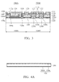
- Fig. 1 shows an illustrative plane view of an inductor according to an embodiment of the invention
- Fig. 2 shows an illustrative cross section of a capacitor-inductor integrated passive component according to an embodiment of the invention
- Fig. 3 shows an illustrative cross section of a capacitor-inductor integrated passive component according to another embodiment of the invention.
- Figs. 4A-4K illustrates a cross section showing the steps for fabricating a capacitor-inductor integrated passive component according to an embodiment of the invention.
- An embodiment of the invention provides an electronic device using a semiconductor substrate and a glass substrate to fabricate a passive component and a fabrication method thereof.
- the embodiment can be used to form an inductor or a metal-insulator-metal (MIM) capacitor individually or to form an inductor-capacitor integrated passive component (L-C IPC) containing the MIM capacitor.
- MIM metal-insulator-metal
- L-C IPC inductor-capacitor integrated passive component
- a cross section of a passive component is shown.
- a plane view of an inductor of the invention is shown in Fig. 1 , which is a spiral inductor.
- a spiral shape of the inductor can be a square-typed spiral shape as shown in Fig. 1 or a circle-type spiral shape.
- a cross section of an inductor along a cross section line 2-2' of Fig. 1 is shown as an inductor area 100B of Fig. 2 . Nevertheless, the inductor area 100B of Fig. 2 only shows a first conductive layer 104b and a second conductive layer 112c of the inductor.
- an electronic device of an embodiment includes a glass substrate 100 and a patterned semiconductor substrate 108, for example a silicon substrate.
- the patterned semiconductor substrate 108 has at least one upper-layered opening, for example a great-sized opening 124 a smaller-sized opening 122 disposed over the glass substrate.
- the electronic device includes at least one passive component, such as a capacitor 200A and/or an inductor 200B, containing first conductive layers 104a and 104b and second conductive layers 112a and 112c, wherein the first conductive layers 104a and 104b are disposed between the semiconductor substrate 108 and the glass substrate 100.
- the second conductive layers 112a and 112c can be disposed in the upper-layered openings 124 and 122 to cooperate with a structure design of the passive component.
- the passive component at the inductor area 100B contains an inductor 200B, in which the first conductive layer 104b is electrically connected to the second conductive layer 112c.
- the passive component at the capacitor area 100A contains a capacitor 200A.
- the capacitor 200A includes a dielectric layer 106a disposed between the semiconductor substrate 108 and the glass substrate 100, and the dielectric layer 106a is combined with the first conductive layer 104a and the second conductive layer 112a to form a sandwich structure.
- the passive component simultaneously includes the capacitor 200A and the inductor 200B.
- the semiconductor substrate 108 contains a first opening 124 corresponding to the capacitor 200A and a second opening 122 corresponding to the inductor 200B, wherein the second conductive layers 112a and 112c are disposed in the first opening 124 and the second opening 122, respectively.
- the second conductive layer 112c at the second opening 122 corresponding to the inductor is electrically connected to the first conductive layer 104b.
- the capacitor contains a dielectric layer 106a disposed between the semiconductor substrate 108 and the glass substrate 100. The second conductive layer 112a at the first opening 124 corresponding to the capacitor is combined with the first conductive layer 104a and the dielectric layer 106a to form a sandwich structure.
- the second opening 122 is smaller than the first opening 124.
- the second conductive layers 112a and 112c are conformally formed in the first opening 124 corresponding to the capacitor and in the second opening 122 corresponding to the inductor, respectively. Because the dielectric layer 106a is a planarization layer, the first conductive layer 104a of the capacitor and the first conductive layer 104b of the inductor are co-planar. Meanwhile, the second conductive layer 112a of the capacitor and the second conductive layer 112c of the inductor are also co-planar.
- the bonding of the semiconductor and the glass substrate can be achieved by an adhesive layer 102, for example a layer made of epoxy resin.
- a first protective layer 110 is conformally formed to cover the semiconductor substrate 108.
- a planarized second protective layer 114 can be formed to cover the second conductive layers 112a and 112c and the first protective layer 110.
- the materials of the first and the second protective layers may be a photosensitive insulating material, for example a photo-resist.
- FIG. 3 a cross section of an electronic device according to another embodiment of the invention is shown.
- the difference between the electronic devices of Fig. 3 and Fig. 2 is that the second conductive layer 112c is formed to fill the second opening 122 corresponding to the inductor in Fig. 3 .
- the first conductive layer 104a is used for a lower electrode layer of the capacitor, thus an upper-layered opening 126 is further formed over the first conductive layer 104a and a conductive layer 112b is formed in the upper-layered opening 126 for connecting the lower electrode layer of the capacitor to an external circuit.
- the glass substrate 100 has a capacitor area 100A and/or an inductor area 100B.
- the patterned semiconductor substrate 108 is disposed over the glass substrate 100.
- the patterned semiconductor substrate 108 has a lower surface 108a and an upper surface 108b.
- a dielectric layer 106a is disposed on the lower surface 108a.
- the dielectric layer 106a may be formed from silicon oxide, silicon nitride, silicon oxynitride or combinations thereof, which can be formed by a thermal oxidation process or a chemical vapor deposition process.
- the thickness of the dielectric layer 106a is about 500 ⁇ to about 1000 ⁇ .
- a plurality of openings 120a and/or 120b is formed in the dielectric layer 106a and the first conductive layers 104a and 104b are formed on the dielectric layer 106a and in the openings 120a and/or 120b of the dielectric layer 106a.
- the first conductive layers 104a and 104b are disposed between the semiconductor substrate 108 and the glass substrate 100.
- an adhesive layer 102 may be used for bonding the semiconductor substrate 108 and the glass substrate 100.
- the material of the adhesive layer 102 may be epoxy resin or other adhesive materials.
- At least one opening is formed on the upper surface 108b of the semiconductor substrate 108 at the inductor area 100B.
- the opening 122 is formed by passing through the semiconductor substrate 108 to expose the first conductive layer 104b in the openings 120b.
- an opening 124 can be formed on the upper surface 108b of the semiconductor substrate 108 at the capacitor area 100A to expose the dielectric layer 106a.
- an opening 126 can be formed on the upper surface 108b of the semiconductor substrate 108 to expose the first conductive layer 104a in the opening 120a.
- the second conductive layers 112a, 112b and 112c can be isolated from the semiconductor substrate 108 by a first protective layer 110.
- the second surface 108b of the semiconductor substrate 108 and the side walls of the openings 122, 124 and 126 are covered with the first protective layer 110.
- the second conductive layers 112a, 112b and 112c are formed on the first protective layer 110 and on the side walls and the bottom surfaces of the openings 122, 124 and 126.
- a second protective layer 114 is formed on the second conductive layers 112a, 112b and 112c and on the first protective layer 110, and portions of the second conductive layers 112a, 112b and 112c are exposed.
- the first conductive layer 104a at the capacitor area 100A, the dielectric layer 106a and the second conductive layer 112a are combined to form a sandwich structure of the capacitor.
- the first conductive layer 104b of the inductor at the inductor area 100B is formed as an inductor winding area of Fig. 1 .
- Two end contacts of the first conductive layer 104b are electrically connected to an external circuit by the second conductive layer 112c.
- the capacitor and the inductor can be integrated to form an inductor-capacitor integrated passive component by a series of connections or a parallel connection.
- the first conductive layers of the capacitor and the inductor are disposed on the same plane, and the second conductive layers of the capacitor and the inductor are also disposed on the same plane, such that a requirement for a flat electronic device is satisfied.
- the materials of the first conductive layer 104 and the second conductive layer 112 may be a low resistance metal layer, for example gold, silver and copper etc., which can be formed by an electroplating process or a deposition process and then patterned by a photolithography and etching process to form the patterns of the first conductive layer 104 and the second conductive layer 112.
- the materials of the first protective layer 110 and the second protective layer 114 may be a photosensitive insulating material, for example photosensitive organic polymer materials.
- the compositions of the photosensitive organic polymer materials may include, but is not limited to, a polyimide (PI), butylcyclobutene (BCB), parylene, polynaphthalenes, fluorocarbons, and accrylates material etc.
- the photosensitive organic polymer materials can be formed by a coating process, such as a spin coating, a spray coating, or a curtain coating process, or other suitable deposition methods. Then, the photosensitive organic polymer materials can be patterned by an exposure and a development process to form the patterns of the first protective layer 110 and the second protective layer 114.
- Figs. 4A-4K show cross sections of the steps for fabricating an electronic device having a passive component according to an embodiment of the invention.
- a semiconductor substrate 108 for example a silicon wafer is provided.
- a dielectric layer 106 is formed on the surfaces of the semiconductor substrate 108.
- the dielectric layer 106 may be planarized silicon oxide layers 106a and 106b formed by a thermal oxidization process.
- the dielectric layer 106 may be formed from silicon nitride or silicon oxynitride by a chemical vapor deposition process.
- at least one lower-layered opening 120 for example the opening 120a at the capacitor area and/or the opening 120b at the inductor area, is formed in the dielectric layer 106a by a photolithography and etching process.
- the first conductive layer 104 is formed on the dielectric layer 106a and in the lower-layered openings 120.
- a metal layer (not shown) is formed on the dielectric layer 106a and in the openings 120 by an electroplating process or a deposition process.
- the metal layer may be formed from copper and has a thickness of about 10 ⁇ m.
- a seed layer for copper electroplating is formed by a deposition process and then a copper layer is coated on the seed layer by an electroplating process to form the metal layer.
- the metal layer is patterned by a photolithography and etching process to form a patterned first conductive layer 104a in the opening 120a of the capacitor area and on the dielectric layer 106a, and to form a patterned first conductive layer 104b in the openings 120b of the inductor area.
- a glass substrate 100 having a thickness of about 400 ⁇ m is provided.
- an adhesive layer 102 may be used for bonding the semiconductor substrate 108 with the glass substrate 100.
- the first conductive layer 104 is disposed between the glass substrate 100 and the semiconductor substrate 108.
- the glass substrate 100 can be reversed and used as a carrier for performing a thinning process to the semiconductor substrate 108.
- the thinning process may be a polishing process or an etching process and the thickness of the semiconductor substrate 108 can be reduced to about several tens of micrometers.
- the dielectric layer 106b on the backside of the semiconductor substrate 108 is removed together.
- At least one upper-layered opening is formed in the semiconductor substrate 108.
- openings 124 and 126 corresponding to the capacitor area 100A and openings 122 corresponding to the inductor area 100B are formed on the upper surface 108b of the semiconductor substrate 108 by a photolithography and etching process.
- the above mentioned openings 122, 124 and 126 are passing through the semiconductor substrate 108, wherein the openings 122 at the inductor area 100B expose the first conductive layer 140b, the opening 124 at the capacitor area 100A exposes the dielectric layer 106a, and the opening 126 at the capacitor area 100A exposes the first conductive layer 140a.
- a protective layer is formed to cover the semiconductor substrate 108.
- a material of a first protective layer 110 such as a photosensitive organic polymer material of polyimide, is coated on the surface of the semiconductor substrate 108 and in the openings 122, 124 and 126 by a coating method.
- the thickness of the first protective layer 110 may be about 5 ⁇ m.
- a photo mask 130 having a photo mask pattern 132 is provided over the first protective layer 110.
- parts of the first protective layer 110 corresponding to the photo mask pattern 132 such as the parts in the openings 122, 124 and 126 are removed to form a patterned first protective layer 110, as shown in Fig. 4H .
- the first protective layer 110 is conformally formed on the surface of the semiconductor substrate 108 and on the side walls of the openings 122, 124 and 126.
- the parts of the first protective layer 110 on the bottoms of the openings 122, 124 and 126 are removed.
- a second conductive layer 112 is formed in the openings 124 and 126 and/or the openings 122.
- a metal layer (not shown) is conformally formed on the surface of the first protective layer 110 and in the openings 122, 124 and 126, covering the side walls and the bottoms of the openings 122 and 124 by an electroplating process or a deposition process. Because the opening 126 is the smallest opening, which can be directly filled with the conductive layer 112b. The opening 126 is disposed corresponding to the conductive layer 104a at the capacitor area which is used for a lower electrode layer of the capacitor.
- the openings 122 are smaller than the opening 124, such that the conductive layer 112c can be conformally formed in the openings 122 corresponding to the inductor area or directly fill up the openings 122.
- the opening 124 can be selected to have a great area.
- the conductive layer 112a can be conformally formed in the opening 124 corresponding to the capacitor area and combined with the dielectric layer 106a and the conductive layer 104a to form a sandwich structure.
- the metal layer may be formed from copper and has a thickness of about 10 ⁇ m.
- a seed layer for copper electroplating is firstly formed by a deposition process and then a copper layer is coated on the seed layer by an electroplating process to form the metal layer. Then, the metal layer is patterned by a photolithography and etching process to form a patterned second conductive layer 112.
- a second protective layer 114 is formed to cover the second conductive layer 112 and the first protective layer 110.
- a material of the second protective layer 114 such as a photosensitive organic polymer material of polyimide is coated on the second conductive layer 112 and the first protective layer 110 and to fill up the openings 122 and/or the opening 124 by a coating method.
- the thickness of the second protective layer 114 may be about 15 ⁇ m.
- a photo mask 140 having a photo mask pattern 142 is provided over the second protective layer 114. After an exposure and development process, parts of the second protective layer 114 corresponding to the photo mask pattern 142 are removed to form a patterned planarized second protective layer 114, as shown in Fig. 4K .
- the patterned planarized second protective layer 114 exposes parts of the second conductive layers 112a, 112b and/or 112c and subsequently forms electrical connection routes to an external circuit for the upper and the lower electrode layers of the capacitor and for the inductor.
- the second protective layer 114 is bonded to a temporary carrier (not shown), for example using a UV curable thin film tape to adhere on the second protective layer 114 for bonding with the temporary carrier.
- a temporary carrier for example using a UV curable thin film tape to adhere on the second protective layer 114 for bonding with the temporary carrier.
- the glass substrate 100 is thinned by a thinning process such as a polishing process or an etching process. The thickness of the glass substrate 100 can be reduced from about 400 ⁇ m to about 200 ⁇ m.
- the temporary carrier is removed and the wafer is diced to separate each electronic device.
- the difference between the electronic devices of Fig. 3 and Fig. 4K is whether the conductive layers 112c fill up the openings 122 corresponding to the inductor area.
- the conductive layer and/or the dielectric layer of the passive component can be formed between the glass substrate and the semiconductor substrate, such that the capacitance density or the quality factor (Q) of the passive component is enhanced.
- the first conductive layer thereof can be used for the lower electrode layers of the capacitor and the inductor simultaneously and disposed on the same plane.
- the second conductive layer also can be formed in the upper-layered openings to form the upper electrode layers of the capacitor and the inductor and disposed on the same plane. Accordingly, the capacitor and the inductor can be flat through the co-planar design for the above mentioned conductive layers.
- the capacitor and/or the inductor can be formed on the high resistance glass substrate, such that the capacitance density or the quality factor (Q) of the capacitor and the inductor are enhanced.
- the capacitance density above about 0.89nF/m 2 can be achieved and the quality factor above about 60 can be achieved.
- the inductor may be a square-shaped spiral inductor has a structure of two and one half of circles. A spiral area of the inductor is about 0.6mm*0.5mm, a width of the electrode layer 104b is about 20 ⁇ m, and a pitch between the electrode layers from a top view is about 20 ⁇ m.
- the inductance value of the inductor at 2.4GHz is about 2.3nH, the quality factor thereof at 2.4GHz is about 31 and the greatest quality factor thereof at 4GHz is about 36.
- the inductor may be a circle-shaped spiral inductor, having a structure of two and one half of circles. A spiral area of the inductor is about 0.6mm*0.5mm, a width of the electrode layer is about 20 ⁇ m, and a pitch between the electrode layers from a top view is about 20 ⁇ m. Accordingly, the inductance value of the inductor at 2.4GHz is about 2.2nH, the quality factor thereof at 2.4GHz is about 34 and the greatest quality factor thereof at 6GHz is about 40.
Landscapes
- Engineering & Computer Science (AREA)
- Power Engineering (AREA)
- Microelectronics & Electronic Packaging (AREA)
- Manufacturing & Machinery (AREA)
- Semiconductor Integrated Circuits (AREA)
- Non-Metallic Protective Coatings For Printed Circuits (AREA)
- Internal Circuitry In Semiconductor Integrated Circuit Devices (AREA)
Applications Claiming Priority (1)
| Application Number | Priority Date | Filing Date | Title |
|---|---|---|---|
| US23564909P | 2009-08-20 | 2009-08-20 |
Publications (2)
| Publication Number | Publication Date |
|---|---|
| EP2287892A2 true EP2287892A2 (de) | 2011-02-23 |
| EP2287892A3 EP2287892A3 (de) | 2012-10-10 |
Family
ID=42735406
Family Applications (1)
| Application Number | Title | Priority Date | Filing Date |
|---|---|---|---|
| EP10172894A Withdrawn EP2287892A3 (de) | 2009-08-20 | 2010-08-16 | Passives Bauelement auf Glassubstrat und Herstellungsverfahren dafür |
Country Status (3)
| Country | Link |
|---|---|
| US (1) | US8766400B2 (de) |
| EP (1) | EP2287892A3 (de) |
| JP (1) | JP5709434B2 (de) |
Cited By (2)
| Publication number | Priority date | Publication date | Assignee | Title |
|---|---|---|---|---|
| WO2013138029A1 (en) * | 2012-03-16 | 2013-09-19 | Qualcomm Mems Technologies, Inc. | High capacitance density metal-insulator-metal capacitors |
| US8896521B2 (en) | 2012-04-24 | 2014-11-25 | Qualcomm Mems Technologies, Inc. | Metal-insulator-metal capacitors on glass substrates |
Families Citing this family (5)
| Publication number | Priority date | Publication date | Assignee | Title |
|---|---|---|---|---|
| TW201226347A (en) * | 2010-12-21 | 2012-07-01 | Chunghwa Picture Tubes Ltd | Method of thinning glass substrate |
| US8624353B2 (en) * | 2010-12-22 | 2014-01-07 | Stats Chippac, Ltd. | Semiconductor device and method of forming integrated passive device over semiconductor die with conductive bridge and fan-out redistribution layer |
| KR101606865B1 (ko) * | 2014-04-28 | 2016-03-28 | 광운대학교 산학협력단 | 포토레지스트 패턴을 이용하는 집적회로 소자의 제조 방법 |
| US11348884B1 (en) * | 2020-11-13 | 2022-05-31 | Taiwan Semiconductor Manufacturing Company Limited | Organic interposer including a dual-layer inductor structure and methods of forming the same |
| US20220375865A1 (en) * | 2021-05-18 | 2022-11-24 | Intel Corporation | Microelectronic assemblies with glass substrates and magnetic core inductors |
Family Cites Families (9)
| Publication number | Priority date | Publication date | Assignee | Title |
|---|---|---|---|---|
| US6399997B1 (en) * | 2000-08-01 | 2002-06-04 | Megic Corporation | High performance system-on-chip using post passivation process and glass substrates |
| JP3462166B2 (ja) * | 2000-09-08 | 2003-11-05 | 富士通カンタムデバイス株式会社 | 化合物半導体装置 |
| JPWO2003007379A1 (ja) | 2001-07-12 | 2004-11-04 | 株式会社日立製作所 | 電子回路部品 |
| WO2004112136A1 (en) * | 2003-06-12 | 2004-12-23 | Koninklijke Philips Electronics N.V. | Electronic device |
| JP4549889B2 (ja) * | 2004-05-24 | 2010-09-22 | 三星モバイルディスプレイ株式會社 | キャパシタ及びこれを利用する発光表示装置 |
| JP4431747B2 (ja) * | 2004-10-22 | 2010-03-17 | 富士通株式会社 | 半導体装置の製造方法 |
| EP1889359B1 (de) * | 2005-06-08 | 2013-01-16 | The Regents of the University of California | Diodenkondensator mit linearvariabler spannung und adaptive anpassungsnetzwerke |
| JP4559993B2 (ja) | 2006-03-29 | 2010-10-13 | 株式会社東芝 | 半導体装置の製造方法 |
| JP5288095B2 (ja) * | 2008-02-07 | 2013-09-11 | ソニー株式会社 | 薄膜トランジスタ基板およびその欠陥修復方法、並びに表示装置 |
-
2010
- 2010-07-26 US US12/843,869 patent/US8766400B2/en active Active
- 2010-08-16 EP EP10172894A patent/EP2287892A3/de not_active Withdrawn
- 2010-08-20 JP JP2010185205A patent/JP5709434B2/ja not_active Expired - Fee Related
Non-Patent Citations (1)
| Title |
|---|
| None |
Cited By (3)
| Publication number | Priority date | Publication date | Assignee | Title |
|---|---|---|---|---|
| WO2013138029A1 (en) * | 2012-03-16 | 2013-09-19 | Qualcomm Mems Technologies, Inc. | High capacitance density metal-insulator-metal capacitors |
| US8896521B2 (en) | 2012-04-24 | 2014-11-25 | Qualcomm Mems Technologies, Inc. | Metal-insulator-metal capacitors on glass substrates |
| US9190208B2 (en) | 2012-04-24 | 2015-11-17 | Qualcomm Mems Technologies, Inc. | Metal-insulator-metal capacitors on glass substrates |
Also Published As
| Publication number | Publication date |
|---|---|
| US20110042783A1 (en) | 2011-02-24 |
| JP2011044716A (ja) | 2011-03-03 |
| JP5709434B2 (ja) | 2015-04-30 |
| EP2287892A3 (de) | 2012-10-10 |
| US8766400B2 (en) | 2014-07-01 |
Similar Documents
| Publication | Publication Date | Title |
|---|---|---|
| US8907447B2 (en) | Power inductors in silicon | |
| JP5234521B2 (ja) | 電子部品及びその製造方法 | |
| CN103985698B (zh) | 具有嵌入式滤波器的多层电子结构 | |
| EP2287892A2 (de) | Passives Bauelement auf Glassubstrat und Herstellungsverfahren dafür | |
| US12237366B2 (en) | Thin film capacitor and electronic circuit substrate having the same | |
| TWI495038B (zh) | 半導體元件以及使用平滑導電層和底側導電層形成整合被動元件結構之方法 | |
| EP1887622A2 (de) | In einen Kondensator integriertes Substrat und Herstellungsverfahren dafür sowie elektronische Komponentenvorrichtung | |
| US8324509B2 (en) | Electronic component and manufacturing method thereof | |
| CN108811319B (zh) | 电子部件及其制造方法 | |
| TW201506969A (zh) | 嵌入在聚合物電介質中的薄膜電容器 | |
| US8907227B2 (en) | Multiple surface integrated devices on low resistivity substrates | |
| JP2002299496A (ja) | 半導体装置及びその製造方法 | |
| CN111403602A (zh) | 垂直电容器结构、电容器组件,以及制造所述垂直电容器结构的方法 | |
| CN113963935A (zh) | 一种电感结构及其制作方法 | |
| KR100766213B1 (ko) | 전자 부품 | |
| JP4367070B2 (ja) | 半導体装置及びその製造方法 | |
| US20060017133A1 (en) | Electronic part-containing elements, electronic devices and production methods | |
| US20210329773A1 (en) | Integrated passive component | |
| US9640477B1 (en) | Semiconductor package and method of producing the semiconductor package | |
| CN101996988B (zh) | 电子装置及其制造方法 | |
| US9929132B2 (en) | Semiconductor device and process of making the same | |
| TWI452673B (zh) | 電子裝置及其製造方法 | |
| JPH0864422A (ja) | インダクター装置 | |
| CN224190811U (zh) | 一种电容芯片结构 | |
| CN117642980A (zh) | 滤波器及其制备方法 |
Legal Events
| Date | Code | Title | Description |
|---|---|---|---|
| PUAI | Public reference made under article 153(3) epc to a published international application that has entered the european phase |
Free format text: ORIGINAL CODE: 0009012 |
|
| AK | Designated contracting states |
Kind code of ref document: A2 Designated state(s): AL AT BE BG CH CY CZ DE DK EE ES FI FR GB GR HR HU IE IS IT LI LT LU LV MC MK MT NL NO PL PT RO SE SI SK SM TR |
|
| AX | Request for extension of the european patent |
Extension state: BA ME RS |
|
| PUAL | Search report despatched |
Free format text: ORIGINAL CODE: 0009013 |
|
| AK | Designated contracting states |
Kind code of ref document: A3 Designated state(s): AL AT BE BG CH CY CZ DE DK EE ES FI FR GB GR HR HU IE IS IT LI LT LU LV MC MK MT NL NO PL PT RO SE SI SK SM TR |
|
| AX | Request for extension of the european patent |
Extension state: BA ME RS |
|
| RIC1 | Information provided on ipc code assigned before grant |
Ipc: H01F 17/00 20060101AFI20120905BHEP Ipc: H01F 41/04 20060101ALI20120905BHEP Ipc: H01L 27/12 20060101ALN20120905BHEP Ipc: H01L 49/02 20060101ALI20120905BHEP |
|
| STAA | Information on the status of an ep patent application or granted ep patent |
Free format text: STATUS: THE APPLICATION IS DEEMED TO BE WITHDRAWN |
|
| 18D | Application deemed to be withdrawn |
Effective date: 20130411 |