EP2287939A1 - Elément électroluminescent organique - Google Patents
Elément électroluminescent organique Download PDFInfo
- Publication number
- EP2287939A1 EP2287939A1 EP08764472A EP08764472A EP2287939A1 EP 2287939 A1 EP2287939 A1 EP 2287939A1 EP 08764472 A EP08764472 A EP 08764472A EP 08764472 A EP08764472 A EP 08764472A EP 2287939 A1 EP2287939 A1 EP 2287939A1
- Authority
- EP
- European Patent Office
- Prior art keywords
- light
- layer
- organic
- organic light
- emitting device
- Prior art date
- Legal status (The legal status is an assumption and is not a legal conclusion. Google has not performed a legal analysis and makes no representation as to the accuracy of the status listed.)
- Withdrawn
Links
Images




Classifications
-
- B—PERFORMING OPERATIONS; TRANSPORTING
- B82—NANOTECHNOLOGY
- B82Y—SPECIFIC USES OR APPLICATIONS OF NANOSTRUCTURES; MEASUREMENT OR ANALYSIS OF NANOSTRUCTURES; MANUFACTURE OR TREATMENT OF NANOSTRUCTURES
- B82Y20/00—Nanooptics, e.g. quantum optics or photonic crystals
-
- B—PERFORMING OPERATIONS; TRANSPORTING
- B82—NANOTECHNOLOGY
- B82Y—SPECIFIC USES OR APPLICATIONS OF NANOSTRUCTURES; MEASUREMENT OR ANALYSIS OF NANOSTRUCTURES; MANUFACTURE OR TREATMENT OF NANOSTRUCTURES
- B82Y30/00—Nanotechnology for materials or surface science, e.g. nanocomposites
-
- C—CHEMISTRY; METALLURGY
- C03—GLASS; MINERAL OR SLAG WOOL
- C03C—CHEMICAL COMPOSITION OF GLASSES, GLAZES OR VITREOUS ENAMELS; SURFACE TREATMENT OF GLASS; SURFACE TREATMENT OF FIBRES OR FILAMENTS MADE FROM GLASS, MINERALS OR SLAGS; JOINING GLASS TO GLASS OR OTHER MATERIALS
- C03C17/00—Surface treatment of glass, not in the form of fibres or filaments, by coating
- C03C17/34—Surface treatment of glass, not in the form of fibres or filaments, by coating with at least two coatings having different compositions
- C03C17/36—Surface treatment of glass, not in the form of fibres or filaments, by coating with at least two coatings having different compositions at least one coating being a metal
- C03C17/38—Surface treatment of glass, not in the form of fibres or filaments, by coating with at least two coatings having different compositions at least one coating being a metal at least one coating being a coating of an organic material
-
- H—ELECTRICITY
- H05—ELECTRIC TECHNIQUES NOT OTHERWISE PROVIDED FOR
- H05B—ELECTRIC HEATING; ELECTRIC LIGHT SOURCES NOT OTHERWISE PROVIDED FOR; CIRCUIT ARRANGEMENTS FOR ELECTRIC LIGHT SOURCES, IN GENERAL
- H05B33/00—Electroluminescent light sources
- H05B33/12—Light sources with substantially two-dimensional [2D] radiating surfaces
- H05B33/22—Light sources with substantially two-dimensional [2D] radiating surfaces characterised by the chemical or physical composition or the arrangement of auxiliary dielectric or reflective layers
-
- H—ELECTRICITY
- H10—SEMICONDUCTOR DEVICES; ELECTRIC SOLID-STATE DEVICES NOT OTHERWISE PROVIDED FOR
- H10K—ORGANIC ELECTRIC SOLID-STATE DEVICES
- H10K50/00—Organic light-emitting devices
- H10K50/10—OLEDs or polymer light-emitting diodes [PLED]
- H10K50/17—Carrier injection layers
-
- H—ELECTRICITY
- H10—SEMICONDUCTOR DEVICES; ELECTRIC SOLID-STATE DEVICES NOT OTHERWISE PROVIDED FOR
- H10K—ORGANIC ELECTRIC SOLID-STATE DEVICES
- H10K59/00—Integrated devices, or assemblies of multiple devices, comprising at least one organic light-emitting element covered by group H10K50/00
- H10K59/80—Constructional details
- H10K59/875—Arrangements for extracting light from the devices
- H10K59/877—Arrangements for extracting light from the devices comprising scattering means
-
- C—CHEMISTRY; METALLURGY
- C03—GLASS; MINERAL OR SLAG WOOL
- C03C—CHEMICAL COMPOSITION OF GLASSES, GLAZES OR VITREOUS ENAMELS; SURFACE TREATMENT OF GLASS; SURFACE TREATMENT OF FIBRES OR FILAMENTS MADE FROM GLASS, MINERALS OR SLAGS; JOINING GLASS TO GLASS OR OTHER MATERIALS
- C03C2217/00—Coatings on glass
- C03C2217/40—Coatings comprising at least one inhomogeneous layer
- C03C2217/43—Coatings comprising at least one inhomogeneous layer consisting of a dispersed phase in a continuous phase
- C03C2217/44—Coatings comprising at least one inhomogeneous layer consisting of a dispersed phase in a continuous phase characterized by the composition of the continuous phase
- C03C2217/445—Organic continuous phases
-
- C—CHEMISTRY; METALLURGY
- C03—GLASS; MINERAL OR SLAG WOOL
- C03C—CHEMICAL COMPOSITION OF GLASSES, GLAZES OR VITREOUS ENAMELS; SURFACE TREATMENT OF GLASS; SURFACE TREATMENT OF FIBRES OR FILAMENTS MADE FROM GLASS, MINERALS OR SLAGS; JOINING GLASS TO GLASS OR OTHER MATERIALS
- C03C2217/00—Coatings on glass
- C03C2217/40—Coatings comprising at least one inhomogeneous layer
- C03C2217/43—Coatings comprising at least one inhomogeneous layer consisting of a dispersed phase in a continuous phase
- C03C2217/46—Coatings comprising at least one inhomogeneous layer consisting of a dispersed phase in a continuous phase characterized by the dispersed phase
- C03C2217/47—Coatings comprising at least one inhomogeneous layer consisting of a dispersed phase in a continuous phase characterized by the dispersed phase consisting of a specific material
- C03C2217/475—Inorganic materials
- C03C2217/479—Metals
-
- C—CHEMISTRY; METALLURGY
- C03—GLASS; MINERAL OR SLAG WOOL
- C03C—CHEMICAL COMPOSITION OF GLASSES, GLAZES OR VITREOUS ENAMELS; SURFACE TREATMENT OF GLASS; SURFACE TREATMENT OF FIBRES OR FILAMENTS MADE FROM GLASS, MINERALS OR SLAGS; JOINING GLASS TO GLASS OR OTHER MATERIALS
- C03C2217/00—Coatings on glass
- C03C2217/40—Coatings comprising at least one inhomogeneous layer
- C03C2217/43—Coatings comprising at least one inhomogeneous layer consisting of a dispersed phase in a continuous phase
- C03C2217/46—Coatings comprising at least one inhomogeneous layer consisting of a dispersed phase in a continuous phase characterized by the dispersed phase
- C03C2217/48—Coatings comprising at least one inhomogeneous layer consisting of a dispersed phase in a continuous phase characterized by the dispersed phase having a specific function
-
- C—CHEMISTRY; METALLURGY
- C03—GLASS; MINERAL OR SLAG WOOL
- C03C—CHEMICAL COMPOSITION OF GLASSES, GLAZES OR VITREOUS ENAMELS; SURFACE TREATMENT OF GLASS; SURFACE TREATMENT OF FIBRES OR FILAMENTS MADE FROM GLASS, MINERALS OR SLAGS; JOINING GLASS TO GLASS OR OTHER MATERIALS
- C03C2217/00—Coatings on glass
- C03C2217/90—Other aspects of coatings
- C03C2217/94—Transparent conductive oxide layers [TCO] being part of a multilayer coating
- C03C2217/948—Layers comprising indium tin oxide [ITO]
-
- H—ELECTRICITY
- H10—SEMICONDUCTOR DEVICES; ELECTRIC SOLID-STATE DEVICES NOT OTHERWISE PROVIDED FOR
- H10K—ORGANIC ELECTRIC SOLID-STATE DEVICES
- H10K2102/00—Constructional details relating to the organic devices covered by this subclass
- H10K2102/301—Details of OLEDs
- H10K2102/331—Nanoparticles used in non-emissive layers, e.g. in packaging layer
-
- H—ELECTRICITY
- H10—SEMICONDUCTOR DEVICES; ELECTRIC SOLID-STATE DEVICES NOT OTHERWISE PROVIDED FOR
- H10K—ORGANIC ELECTRIC SOLID-STATE DEVICES
- H10K85/00—Organic materials used in the body or electrodes of devices covered by this subclass
- H10K85/10—Organic polymers or oligomers
- H10K85/111—Organic polymers or oligomers comprising aromatic, heteroaromatic, or aryl chains, e.g. polyaniline, polyphenylene or polyphenylene vinylene
- H10K85/113—Heteroaromatic compounds comprising sulfur or selene, e.g. polythiophene
- H10K85/1135—Polyethylene dioxythiophene [PEDOT]; Derivatives thereof
Definitions
- the present invention relates to one of organic semiconductor devices, which utilizes an organic compound which exhibits electroluminescence (hereinafter referred to as EL) when electric current is caused to flow thereinto, and particularly an organic light-emitting device comprising an organic light-emitting layer made of such an EL organic compound.
- EL electroluminescence
- an organic light-emitting device using an EL organic compound material is an electric current-injection type device having characteristics of a diode.
- a display panel comprising organic light-emitting devices that emit light of two or more luminescent colors and are laid out in a matrix form.
- each of the organic light-emitting devices 1 is composed of e.g., on a transparent substrate 2, a transparent anode 3, plural organic compound material layers 4 including a light-emitting layer, and a reflective metallic cathode 5, which are serially formed by using a vacuum evaporation method or the like.
- the organic compound material layers 4 have functional layers sandwiching the light-emitting layer, i.e., appropriate hole transport functional layers (e.g., a hole injection layer, a hole transport layer) on the anode side and appropriate electron transport functional layers (e.g., an electron injection layer, an electron transport layer) on the cathode side.
- an organic EL display apparatus there may be a contrast deterioration of the panel at a light-place due to a high reflectance of the cathode made of A1 or the like in the organic light-emitting device. Therefore there is a suggestion that a circular polarized light filter is adhered on the transparent substrate on the side of extracting EL emissions to the outside (see Patent Literature 1). Further, there is another suggestion of a configuration of the organic EL display apparatus in which its light absorption layer is made of a matrix material includes metal nanoparticles and disposed near to the electrode to improve the contrast of organic EL display apparatus (see Patent Literature 2).
- the circular polarized light plate can cut off ambient light, but bring a problem of decrease of EL emission intensity.
- the inventor has revealed that a light extraction yield is insufficient in the organic EL display apparatus using the light absorption layer including metal nanoparticles in the light extraction side.
- an organic light-emitting device with a simple configuration that is capable of cutting off ambient light while keeping an emission intensity in EL light (EL luminance) higher than that of the device using the circular polarized light filter, by using the light-scattering technology and light canceling technology for a transparent members therein.
- EL luminance emission intensity in EL light
- An organic light-emitting device is an organic light-emitting device comprising: a pair of first and second electrodes opposed to each other; and a plurality of organic semiconductor layers layered and disposed between the first and second electrodes, wherein the organic semiconductor layers include an organic light-emitting layer, the organic semiconductor device further comprising a light-scattering layer layered and disposed between the organic light-emitting layer and at least one of the first and second electrodes.
- the light-scattering layer includes: organic materials having carrier injection and transport characteristics of transporting electrons and/or holes; and plural particles dispersed among the organic materials so that light emitted from the organic light-emitting layer is passed therethrough.
- the light-scattering layer is introduced into the device; it reduces an interference effect so that settings of elements are allowed in a status unrestricted relatively. Therefore, the present invention will provide a device with an emission yield higher than that of the device using the circular polarized light filter even under there is a large thickness of the organic layers.
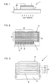
- FIG. 2 is a rear view of a partially enlarged portion of a passive driven type organic EL display panel to which a plurality of organic light-emitting devices are applied as an example of display panels.
- pluralities of light-emitting devices 1 are arranged in a matrix shape on a substrate 45.
- This organic EL display panel comprises a plurality of first electrodes 46 of row electrodes that contain transparent electrode layers; organic semiconductor layers; and a plurality of second electrodes 52 of column electrodes that contain metal electrode layers each intersecting the row electrodes, in which the first electrodes, the organic semiconductor layers and the second electrodes are layered sequentially on the substrate 45.
- the row electrodes are each formed in a strip shape, and are arranged parallel to one another with a predetermined spacing therebetween; likewise the column electrodes.
- the matrix display panel comprises a displaying region DR constructed from emitters of the organic light-emitting devices 1 which are formed at the points of intersection between plural row electrodes and plural column electrodes respectively.
- the second electrodes 52 are connected via connection portions Cn to wiring electrodes 19 respectively.
- s sealing film (not shown) is formed on and over the second electrodes 15, which is an inorganic passivation film made of inorganic, e.g., nitrides such as silicon oxynitride, silicon nitride and the like or oxides or carbides and the like.
- the sealing film of inorganic passivation film may be formed as a multilayer film including synthetic resin films layered by turns therebetween such as fluorocarbon polymers, silicone polymers, photo-resists, polyamides and the like, thereby the organic light-emitting devices are cut off from the air.
- the organic light-emitting layers may be made of organic compound materials exhibiting red, green and blue emissions with electric current applications respectively. In other words, the organic light-emitting devices are formed up as appropriate so as to constitute red, green and blue luminescent parts.
- the organic light-emitting device may be constructed as a bottom emission type one in which luminescent light is took out form the substrate 45 made of a transparent material on which a transparent electrode of the first electrode is formed and the second electrode is a metallic electrode, and alternatively the organic light-emitting device may be constructed as a top emission type one in which the first electrode is ametallic electrode and the second electrode is a transparent electrode.
- Fig. 3 shows a basic organic semiconductor layers 40 for example, in which plural organic material films having functions respectively are layered in turn between from an anode of the first electrode 46 to a cathode of the second electrode 52 as follows: hole injection layer 47 / hole transport layer 48 / light-emitting layer 49 / electron transport layer 50 / electron injection layer 51, wherein "/" denotes an interface as a partition between layers.
- an electron blocking layer may be layered between the hole transport layer and the light-emitting layer as an organic material film, and also a hole blocking layer may be layered between the light-emitting layer and the electron transport layer as an organic material film.
- the organic light-emitting device may have a configuration including a layer in which electrical carriers and excitons dispersed therein in order to shut electrical carriers and excitons in the light-emitting layer 49.
- there may be omitted any one of the hole injection layer, the hole transport layer, the electron transport layer, the electron injection layer, the electron blocking layer and the hole blocking layer, excepting the light-emitting layer.
- the bottom emission type of a basic organic light-emitting device shown in the figure comprises a first electrode 46, organic semiconductor layers 40 including an organic light-emitting layer 49, and a second electrode 52 which are layered sequentially from the side of the substrate 45, light extraction is preformed on the side of the substrate 45.
- the first electrode 46 and the second electrode 52 are the anode and the cathode respectively.
- holes are injected from the first electrode 46 of the anode, electrons are injected from the second electrode 52 of the cathode into the light-emitting layer mainly made of organic compounds of the organic semiconductor layers 40, so that electrons and holes recombine, and light is produced.
- Fig. 4 is a schematic image diagram showing a cross-section of one example of an organic light-emitting device shown in Fig. 3 for explaining typical optical paths. In the figure, gaps are drawn between the layers, since only the figure of being easily observed is taken into consideration.
- the organic light-emitting device 1 has a configuration, on the glass substrate, the transparent anode 46, the hole injection layer 47, the hole transport layer 48, the light-emitting layer 49, the electron transport layer 50, the electron injection layer 51 and the metal cathode 52 are layered in turn.
- the EL emission is preformed in various directions due to the recombination of electrons and holes in the light-emitting layer 49 of the organic light-emitting device.
- Each light ray at each emission site is produced in the light-emitting layer 49 on the optical path as follows:
- the light ray L1 (less than a critical angle on each interface) toward the anode 46 passes through the organic semiconductor layers 40 and the transmissive anode 46 to go out the organic light-emitting device as a output.
- the light ray L2 toward the cathode 52 is reflected by the cathode 52, and passes through all of the organic semiconductor layers 40 and the anode 46 to go out the organic light-emitting device as a output (less than a critical angle on each interface).
- the rest of light L3 (a critical angle or more on each interface) emitted by the light-emitting layer 49 vanishes from the organic light-emitting device without extraction out of the organic light-emitting device to the outside.
- the substrate 45 is made of a transparent substance such as glass, plastics or like, alternatively, may be of a semi-transparent or opaque material.
- the anode 46 is made of an oxide such as ITO (Indium Tin Oxide), IZO (Indium Zinc Oxide), Tin Oxide or the like of transparent materials.
- the anode 46 may be a thin film made of gold, palladium or the like such as Au, Ag, Cu, Si, Pt, Pd and the like or an alloy thereof.
- the anode 46 may be made of A1, Mo, Ti or the like.
- a material of the anode 46 may be conductive carbon, polyanilines, polythiophenes, polypyrroles or the like of n-conjugated polymers or the like.
- a material of the cathode 52 may be a substance with a low work function employed for the interface in contact with the organic semiconductor layers 40 such as alkaline metal, Lithium, Sodium or the like, or, alkaline-earth metal i.e., Group IIA, Beryllium, Magnesium, Calcium, Barium or the like, or, Group III metal including rare earth metals such as Scandium, Yttrium, Lanthanum, cerium, Europium, Terbium or the like, or, Actinides metal such as Actinium or the like, or, an alloy of those, but not limited to those materials.
- the cathode 52 may be formed as a multilayered film layered or composed of a substance layer with a low work function and the other metal layer that is employed for the interface in contact with the organic semiconductor layers 40.
- the hole injection layer 47 has a function for facilitating to extract holes from the anode 46.
- This hole injection layer 47 may be, for example, made of one of materials of, specifically is not limited thereto, metal phthalocyanines such as CuPc (Copper Phthalocyanine) or the like or inorganic phthalocyanines, carbon films, PEDOT (i.e., Poly (3,4-ethylenedioxythiophene)), polyanilines, Poly (p-phenylenevinylene) derivatives, polythiophene derivatives, Poly-p-phenylene derivatives, Polyalkylphenylene derivatives, polyacetylene derivatives or the like preferably.
- metal phthalocyanines such as CuPc (Copper Phthalocyanine) or the like or inorganic phthalocyanines
- carbon films PEDOT (i.e., Poly (3,4-ethylenedioxythiophene)), polyanilines, Poly (p-phenylenevinylene) derivatives, polythiophene derivatives,
- the hole transport layer 48 has a function for transporting holes to the organic light-emitting layer 49, these holes extracted by the hole injection layer 47 from the anode 46.
- This hole transport layer 48 may be made of, for example, one of organic compounds capable of transporting holes, such as N, N, N', N'-tetraphenyl-4, 4'-diaminophenyl, N, N'-diphenyl-N, N'-di(3-methylphenyl)-4, 4'-diaminobiphenyl, 2, 2-bis(4-di-p-tolylaminophenyl)propane, N, N, N', N'-tetra-p-tolyl-4, 4'-diaminobiphenyl, Bis(4-di-p-tolylaminophenyl)phenylmethane, N, N'-diphenyl-N, N'-di(4-methoxyphenyl)-4, 4'-diamin
- the light-emitting layer 49 is equivalent to a photoelectric conversion layer that has a function for emitting light by an electric field caused by a voltage applied across the first and second electrodes.
- the light-emitting layer 49 utilizes a light emission phenomenon based on the energy received with the outside electric field to emit light itself.
- the electron transport layer 50 has a function for effectively transporting electrons to the light-emitting layer 49, these electrons extracted by the electron injection layer 51 from the cathode 52.
- organic compounds capable of transporting electrons and a main component used for the light-emitting layer 49 or the electron-transporting organic semiconductor layer are as follows: polycyclic compounds such as p-terphenyl, quaterphenyl as well as derivatives thereof, condensed polycyclic hydrocarbon compounds such as naphthalene, tetracene, pyrene, coronene, chrysene, anthracene, diphenylanthracene, naphthacene, phenanthrene as well as derivatives thereof, condensed heterocyclic compounds such as phenanthroline, bathophenanthroline, phenanthridine, acridine, quinoline, quinoxaline, phenazine and the like as well as derivatives thereof, andfluoroceine, perylene,
- metal- chelated complex compounds specifically suitable metal-chelated oxanoide compounds are metal complexes which contain, as a ligand thereof, at least one selected from 8-quinolinolato and derivatives thereof such as tris(8-quinolinolato)aluminum, which is a fluorescent substance, bis(8-quinolinolato)magnesium, bis[benzo(f)-8-quinolinolato] zinc, bis(2-methyl-8-quinolinolato)aluminum, tri(8-quinolino lato)indium, tris(5-methyl-8-quinolinolato)aluminum, 8-quinolinolatolithium, tris(5-chloro-8-quinolinolato)gallium, and bis(5-chloro-8-quinolinolato)calcium.
- 8-quinolinolato and derivatives thereof such as tris(8-quinolinolato)aluminum, which is a fluorescent
- organic compounds capable of transporting electrons such as oxadiazoles, triazines, stilbene derivatives and distyrylarylene derivatives, styryl derivatives, diolefin derivatives can be used preferably for the device.
- organic compounds capable of transporting electrons used for the device are as follows: the group of benzoxazoles such as 2, 5-bis(5, 7-di-t-pentyl-2-benzoxazolyl)-1, 3, 4-thiazole, 4, 4'-bis(5, 7-t-pentyl-2-benzoxazolyl)stilbene, 4, 4'-bis[5, 7-di(2-methyl-2-butyl)-2-benzoxazolyl]stilbene, 2, 5-bis(5, 7-di-t-pentyl-2-benzoxazolyl)thiophene, 2, 5-bis[5-( ⁇ , ⁇ -dimethylbenzyl)-2-benzoxazolyl]thiophene, 2,5-bis[5,7-di(2-methyl-2butyl)-2-benzoxazolyl]-3,4-diphenyl thiophene, 2, 5-bis(5-methyl-2-benzoxazolyl)thiophene, 4, 4'-bis(2-benzoxazo
- organic compounds capable of transporting electrons used for the device are as follows: 1, 4-bis(2-methylstyryl)benzene, 1, 4-bis(3-methylstyryl)benzene, 1, 4-bis(4-methylstyryl)benzene, distyrylbenzene, 1, 4-bis(2-ethylstyryl)benzene, 1, 4-bis(3-ethylstyryl)benzene, 1, 4-bis(2-methylstyryl)-2-methylbenzene, 1, 4-bis(2-methylstyryl)-2-ethylbenzene or the like.
- organic compounds capable of transporting electrons used for the device are as follows: 2, 5-bis(4-methylstyryl) pyrazine, 2, 5-bis(4-ethylstyryl)pyrazine, 2, 5-bis[2-(1-naphthyl)vinyl]pyrazine, 2, 5-bis(4-methoxystyryl)pyrazine, 2, 5-bis[2-(4-biphenyl)vinyl]pyrazine, 2, 5-bis[2-(1-pyrenyl)vinyl]pyrazine or the like.
- organic compounds capable of transporting electrons used for the device are as follows: 1, 4-phenylene-dimethylidine, 4, 4'-phenylenedimethylidine, 2, 5-xylylene-dimethylidine, 2, 6-naphthylenedimethylidine, 1, 4-biphenylene-dimethylidine, 1, 4-p-terephenylenedimethylidine, 9, 10-anthracenediyldimethylidine, 4, 4'-(2, 2-di-t-butylphenylvinyl)biphenyl, 4, 4'-(2, 2-diphenylvinyl)biphenyl or the like.
- any of the well-known compounds conventionally used in the production of the prior art organic EL devices may be suitably used for the device.
- Each of the organic semiconductor layers 40 is made of organic substances of small-molecules, or dendrimers of macromolecules.
- the organic semiconductor layers 40 made of small-molecule organic compounds are formed in general by a vacuum evaporation method or the like as a dry process (vacuum process), and the organic semiconductor layers 40 made of polymers or dendrimers of organic compounds are formed in general by a coating method.
- a vacuum evaporation method or the like as a dry process (vacuum process)
- the organic semiconductor layers 40 made of polymers or dendrimers of organic compounds are formed in general by a coating method.
- materials of the light-emitting layer and the like used for the organic semiconductor layers 40 are belong to a P-type organic semiconductor, N-type organic semiconductor or a bipolar-type organic semiconductor.
- the precursors thereof are dissolved in pertinent solvents respectively and the resultant solutions are coated.
- solvents there is used for one or more solvents selected from solvents such as toluene, benzene, chlorobenzene, dichlorobenzene, chloroform, Tetralin, xylene, Anisole, dichloromethane, ⁇ butyrolactone, butyl Cellosolve, cyclohexane, NMP (N-methyl-2-pyrrolidone), dimethyl sulfoxide, cyclohexanone, dioxane, or THF (tetrahydrofuran), or the like.
- solvents such as toluene, benzene, chlorobenzene, dichlorobenzene, chloroform, Tetralin, xylene, Anisole, dichloromethane, ⁇ butyrolactone, butyl Cellosolve, cyclohexane, NMP (N-methyl-2-pyrrolidone), di
- solvents such as PGME (propyleneglycol monomethyl ether), PGMEA (propyleneglycol monomethyl ether acetate), Ethyl lactate, DMAc (N. N-dimethylacetamide), MEK (methyl ethyl ketone) , MIBK (methyl isobutyl ketone), PSS (polystyrenesulfonate), IPA (iso propyl alcohol), ethanol and the like can be used.
- PGME propyleneglycol monomethyl ether
- PGMEA propyleneglycol monomethyl ether acetate
- Ethyl lactate DMAc (N. N-dimethylacetamide)
- MEK methyl ethyl ketone
- MIBK methyl isobutyl ketone
- PSS polystyrenesulfonate
- IPA iso propyl alcohol
- the whole surface coating method for the substrate 45 such as a spin coating method, a blade coating method, a roll coating method, a spray coating method and the like, and the printing method such as a ink jet method, a flexo print process, a dispenser method and the like, and a predetermined patterned coating method.
- Fig. 5 is a schematic image diagram showing a cross-section of an organic light-emitting device of Example NP for explaining typical optical paths. In the figure, gaps are drawn between the layers, since only the figure of being easily observed is taken into consideration.
- the organic light-emitting device 1 has a configuration, on the glass substrate, the transparent anode 46, the light-scattering layer 47a of the hole injection layer in which plural particles are dispersed, the hole transport layer 48, the light-emitting layer 49, the electron transport layer 50, the electron injection layer 51 and the metal cathode 52 are layered in turn.
- the light-scattering layer 47a is a thin film comprising a base material of the hole injection layer prepared to have a transmittance and to reflect partially light; and particles dispersed therein.
- Each particle has an acicular shape, cylinder shape, plate shape, rectangular parallelepiped shape, cube shape, cone shape, spherical shape, prism shape, or the like as an individual, or aggregation thereof.
- the particles have an average particle size ranging from 0.1nm to 10000nm.
- the radiuses of dispersed particle are extremely considerably small in comparison with wavelengths of entering ambient light, and the particle size distribution of the dispersed particles is set so as to generate the Rayleigh scattering.
- the particles are dispersed at a density so that a distance between adjacent particles is within a range of 0.1nm or more and 1 ⁇ m or less.
- Material of particles is selected to have a refractive index satisfying a refractive index difference of 0.01 or more different from a refractive index of the organic materials of the organic semiconductor layer.
- the light-scattering layer 47a has an uneven or rough interface with a difference of elevation of 0.1nm or more and 1000nm or less.
- the light-scattering layer 47a is set to have a carrier mobility of 1 ⁇ 10 -10 - 1 ⁇ 10 10 cm 2 /Vs, or a conductivity of 10 10 - 10 -10 ⁇ cm.
- the hole transport layer may be used as a light-scattering layer using dispersed particles therein or the like.
- the light-scattering layer may be layered and disposed anywhere between the organic light-emitting layer 49 and the anode 46 as an organic semiconductor layer.
- the optical paths of EL emission light and ambient light in the light-emitting layer 49 of the organic light-emitting device shown in Fig. 5 are similar to those of the organic light-emitting device shown in Fig. 4 , but, somewhat light within the light rays toward the anode 46, e.g., the light ray travelling along with the light-emitting layer 49 is scattered by the Rayleigh scattering of the light-scattering layer 47a. The scattered light ray goes out from the anode 46 to the outside of the organic light-emitting device as an output light. Since the light-scattering layer 47a improves the light extraction yield of the organic light-emitting device, the amount of light emission throughout the device increases.
- respective layers' refractive indexes are set as mentioned above so that lateral light propagation is restrained, resulting in improvement of a further light extraction yield.
- the intensity of scattered light due to Rayleigh scattering is inversely proportional to the fourth power of wavelength of ambient light
- Fig. 6 is a schematic image diagram showing a cross-section of an organic light-emitting device of Example BL for explaining typical optical paths. In the figure, gaps are drawn between the layers, since only the figure of being easily observed is taken into consideration.
- the organic light-emitting device 1 has a configuration, on the glass substrate, the transparent anode 46, the hole injection layer 47, the semi-transparent metal layer 99, the hole transport layer 48, the light-emitting layer 49, the electron transport layer 50, the electron injection layer 51 and the metal cathode 52 are layered in turn.
- the semi-transparent metal layer 99 is formed between the hole injection layer 47 and the hole transport layer 48.
- the semi-transparent metal layer 99 may be at least one thin film prepared to have a transmittance and to reflect light partially, for example, Ag and MoO 3 are contained therein.
- the semi-transparent metal layer 99 may be, for example, silver alloy thin film.
- metal for the layer alloy is not limited to silver, but gold may be employed for the layer alloy, for example.
- Oxide for the layer alloy is not limited to Mo oxide, but transition metal oxide may be employed for the layer alloy, for example.
- the semi-transparent metal layer 99 is deposited at a thickness in a range of 10nm or more and 50nm or less.
- the semi-transparent metal layer 99 is a transparent or semi-transparent thin film, having a high reflectance preferably, and having a refractive index lower than that of the adjacent layer preferably.
- a simple substance film such as Ag, Au, Cu, Al, Pt, Mg, and an alloy-based thin film such as MgAg, MgAu and the like, an oxide thin film, a fluoride thin film, a mixture-based thin film made of oxide, fluoride and metal or the like may be employed for the semi-transparent metal layer 99.
- an Ag-, Ag alloy-, or Mg alloy-based thin film has a high reflectance.
- An Ag bulk has a low refractive index of 1 or less.
- These thin films made of metal, or alloy-material may be used for a semi-transparent with 10nm or more 50nm or less in thick, for example.
- the an oxide thin film, the fluoride thin film, and the mixture-based thin film made of oxide, fluoride and metal may have a high transparency, so that its thickness is not limited.
- these thin films are prepared to have 10nm or less in thick and exhibit the surface roughness (interfaces are uneven). As a result, laterally propagated light is scattered toward the front face due to the surface roughness.
- the Au layer with a 3nm thickness disposed on the substrate 45 has the surface roughness of 2.6nm.
- the semi-transparent metal layer 99 is prepared to have a thickness of, for example 10-50nm, its transmittance is 1%-99% or less in a visible wavelength band of 400nm-700nm. Therefore, specifically 10-90%, more specifically 20-70% of transmittance of the layer 99 is obtained by the thickness settings. Further, the reflectance of the semi-transparent metal layer 99 may be obtained of 1%-99% or less, specifically 5-95%, more specifically 10-70% in the visible wavelength band of 400nm-700nm, by the thickness settings.
- the light-emitting layer 49 is prepared to have a refractive index equal to or less than that of the adjacent layer preferably.
- the optical paths of EL emission light and ambient light in the light-emitting layer 49 of the organic light-emitting device shown in Fig. 6 are similar to those of the organic light-emitting device shown in Fig. 4 , but, a contrast of the device increases , particularly, at a light-place in response to the intensity ratio between the reflected ambient light E1 and the EL emission light of the light-emitting layer 49.
- Fig. 7 is a schematic image diagram showing a cross-section of an organic light-emitting device of Example BL1 for explaining typical optical paths. In the figure, gaps are drawn between the layers, since only the figure of being easily observed is taken into consideration.
- the organic light-emitting device 1 has a configuration, on the glass substrate, the transparent anode 46, the light-scattering layer 47a of the hole injection layer in which plural particles are dispersed, the semi-transparent metal layer 99, the hole transport layer 48, the light-emitting layer 49, the electron transport layer 50, the electron injection layer 51 and the metal cathode 52 are layered in turn.
- Example BL1 of the organic light-emitting device has a configuration so that the semi-transparent metal layer 99 (disposed between the light-scattering layer 47a and the hole transport layer 48) is added to Fig. 5 's Example NP of the organic light-emitting device having the light-scattering layer 47a.
- the semi-transparent metal layer 99 has a transmittance and to reflect partially light, and may be at least one thin film that Ag and MoO 3 are contained therein similarly to Fig. 6 's Example BL.
- the optical paths of EL emission light and ambient light in the light-emitting layer 49 of the organic light-emitting device shown in Fig. 7 are similar to those of the organic light-emitting device shown in Figs. 5 and 6 , but, somewhat light within the light rays toward the anode 46, e.g., the light ray travelling along with the light-emitting layer 49 and passing through the semi-transparent metal layer 99 is scattered by the Rayleigh scattering of the light-scattering layer 47a. The scattered light ray goes out from the anode 46 to the outside of the organic light-emitting device as an output light. Since the light-scattering layer 47a improves the light extraction yield of the organic light-emitting device, the degree of contrast throughout the device increases.
- Fig. 8 is a schematic image diagram showing a cross-section of an organic light-emitting device of Example BL2 for explaining typical optical paths. In the figure, gaps are drawn between the layers, since only the figure of being easily observed is taken into consideration.
- the organic light-emitting device 1 has a configuration, on the glass substrate, the transparent anode 46, the particulate film 100 containing plural particles, the hole injection layer 47, the hole transport layer 48, the light-emitting layer 49, the electron transport layer 50, the electron injection layer 51 and the metal cathode 52 are layered in turn.
- Fig. 8 's Example BL2 of the organic light-emitting device is the same as Fig.
- the particulate film 100 is deposited between the anode 46 and the hole injection layer 47.
- the particulate film 100 is a thin film containing plural particles and prepared to have a transmittance and to reflect light partially.
- the particles of the particulate film 100 are made of oxide, complex oxide, fluoride, or metal, and the particulate film 100 is a cohesion film in which the particles cohered with an organic binder.
- the particulate film 100 may be used in a fashion of combined plural cohesion films.
- the particulate film 100 is deposited and formed at a thickness of a range 10-50nm.
- the optical paths of EL emission light and ambient light in the light-emitting layer 49 of the organic light-emitting device shown in Fig. 8 are similar to those of the organic light-emitting device shown in Fig. 4 , but, a contrast of the device increases, particularly, at a light-place in response to the intensity ratio between the reflected ambient light E1 and the EL emission light of the light-emitting layer 49.
- Plasmon can couple with a photo electric field in a visible to near infrared wavelength range in the metal, so that specific photo energies are absorbed, whereby the Plasmon plays a brilliant role in tone of color of the metal.
- the Plasmon can be described as a collective oscillation of free electrons in metal and then the plasmons are localized at the surface in metal nanoparticles.
- This Surface Plasmon Resonance (SPR) generates an enhanced electric field remarkably localized.
- conversion from photo energies to the surface plasmon contributes accumulation of photo energies on the surface of metal nanoparticles and enables to control light at a minute region small than a diffraction limit of light.
- Fig. 9 is a schematic image diagram showing a cross-section of an organic light-emitting device of Example BL3 for explaining typical optical paths. In the figure, gaps are drawn between the layers, since only the figure of being easily observed is taken into consideration.
- the organic light-emitting device 1 has a configuration, on the glass substrate, the transparent anode 46, the particulate film 100 containing plural particles, the hole injection layer 47, the semi-transparent metal layer 99, the hole transport layer 48, the light-emitting layer 49, the electron transport layer 50, the electron injection layer 51 and the metal cathode 52 are layered in turn.
- Example BL3 of the organic light-emitting device has a configuration so that the semi-transparent metal layer 99 (disposed between the hole injection layer 47 and the hole transport layer 48) is added to Fig. 8 's Example BL2 of the organic light-emitting device having the light-scattering layer 47a.
- the semi-transparent metal layer 99 has a transmittance and to reflect partially light, and may be at least one thin film that Ag and MoO 3 are contained therein similarly to Fig. 6 's Example BL.
- the optical paths of EL emission light and ambient light in the light-emitting layer 49 of the organic light-emitting device shown in Fig. 9 are similar to those of the organic light-emitting device shown in Fig. 8 , but, a contrast of the device increases, particularly, at a light-place in response to the intensity ratio between the reflected ambient light E1 and the EL emission light of the light-emitting layer 49.
- Fig. 10 is a schematic image diagram showing a cross-section of an organic light-emitting device of Example BL4 for explaining typical optical paths. In the figure, gaps are drawn between the layers, since only the figure of being easily observed is taken into consideration.
- the organic light-emitting device 1 has a configuration, on the glass substrate, the transparent anode 46, the particulate film 100 containing plural particles, the light-scattering layer 47a of the hole injection layer in which plural particles are dispersed, the hole transport layer 48, the light-emitting layer 49, the electron transport layer 50, the electron injection layer 51 and the metal cathode 52 are layered in turn.
- Example BL4 of the organic light-emitting device has a configuration so that the particulate film 100 (disposed between the anode 46 and the light-scattering layer 47a) is added to Fig. 5 's Example NP of the organic light-emitting device having the light-scattering layer 47a.
- the particulate film 100 is a thin film, similarly to Fig. 8 's Example BL2, containing plural particles and prepared to have a transmittance and to reflect light partially.
- the optical paths of EL emission light and ambient light in the light-emitting layer 49 of the organic light-emitting device shown in Fig. 10 are similar to those of the organic light-emitting device shown in Figs. 5 and 6 , but, somewhat light within the light rays toward the anode 46, e.g., the light ray travelling along with the light-emitting layer 49 is scattered by the Rayleigh scattering of the light-scattering layer 47a.
- the scattered light ray passes through the particulate film 100 and goes out from the anode 46 to the outside of the organic light-emitting device as an output light. Since the light-scattering layer 47a and the particulate film 100 improve the light extraction yield of the organic light-emitting device, the degree of contrast throughout the device increases.
- Fig. 11 is a schematic image diagram showing a cross-section of an organic light-emitting device of Example BL5 for explaining typical optical paths. In the figure, gaps are drawn between the layers, since only the figure of being easily observed is taken into consideration.
- the organic light-emitting device 1 has a configuration, on the glass substrate, the transparent anode 46, the particulate film 100 containing plural particles, the light-scattering layer 47a of the hole injection layer in which plural particles are dispersed, the semi-transparent metal layer 99, the hole transport layer 48, the light-emitting layer 49, the electron transport layer 50, the electron injection layer 51 and the metal cathode 52 are layered in turn.
- Example BL5 of the organic light-emitting device has a configuration so that the particulate film 100 (disposed between the anode 46 and the light-scattering layer 47a) and the semi-transparent metal layer 99 (disposed between the light-scattering layer 47a and the hole transport layer 48) are added to Fig. 5 's Example NP of the organic light-emitting device having the light-scattering layer47a.
- the particulate film 100 is a thin film, similarly to Fig. 8 's Example BL2, containing plural particles and prepared to have a transmittance and to reflect light partially.
- the semi-transparent metal layer 99 has a transmittance and to reflect partially light, and may be at least one thin film that Ag and MoO 3 are contained therein similarly to Fig. 6 's Example BL.
- the optical paths of EL emission light and ambient light in the light-emitting layer 49 of the organic light-emitting device shown in Fig. 11 are similar to those of the organic light-emitting device shown in Figs. 5 and 6 , but, somewhat light within the light rays toward the anode 46, e.g., the light ray travelling along with the light-emitting layer 49 passes through the semi-transparent metal layer 99 and is scattered by the Rayleigh scattering of the light-scattering layer 47a. The scattered light ray passes through the particulate film 100 and goes out from the anode 46 to the outside of the organic light-emitting device as an output light. Since the light-scattering layer 47a and the particulate film 100 improve the light extraction yield of the organic light-emitting device, the degree of contrast throughout the device increases.
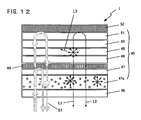
- Fig. 12 is a schematic image diagram showing a cross-section of an organic light-emitting device of Example BL6 for explaining typical optical paths.
- the organic light-emitting device 1 has a configuration, on the glass substrate, the transparent anode 46, the light-scattering layer 47a of the hole injection layer in which plural particles are dispersed, the hole injection layer 47, the semi-transparent metal layer 99, the hole transport layer 48, the light-emitting layer 49, the electron transport layer 50, the electron injection layer 51 and the metal cathode 52 are layered in turn.
- Example BL6 of the organic light-emitting device has a configuration so that the hole injection layer 47 (disposed between the semi-transparent metal layer 99 and the light-scattering layer 47a) is added to Fig. 7 's Example BL1 of the organic light-emitting device having the light-scattering layer 47a.
- the semi-transparent metal layer 99 has a transmittance and to reflect partially light, and may be at least one thin film that Ag and MoO 3 are contained therein similarly to Fig. 6 's Example BL.
- the optical paths of EL emission light and ambient light in the light-emitting layer 49 of the organic light-emitting device shown in Fig. 12 are similar to those of the organic light-emitting device shown in Figs. 5 and 6 , but, somewhat light within the light rays toward the anode 46, e.g., the light ray travelling along with the light-emitting layer 49 passes through the semi-transparent metal layer 99 and is scattered by the Rayleigh scattering of the light-scattering layer 47a. The scattered light ray goes out from the anode 46 to the outside of the organic light-emitting device as an output light. Since the light-scattering layer 47a improves the light extraction yield of the organic light-emitting device, the degree of contrast throughout the device increases.
- ITO Indium Tin Oxide
- NPB naphthylpentylbenzidine
- Alq3 tris(8-hydroxyquinolinato)aluminium, a green luminescence dye
- Example ref' with a polarizing plate > A organic EL device with a configuration of glass substrate / transparent electrode / hole transport layer / organic light-emitting layer / electron injection layer / reflective electrode / was fabricated.
- Example ref of the organic EL device was fabricated and then, a polarizing plate was adhered on its glass substrate.
- Example NP-t> A organic EL device with a configuration of glass substrate / transparent electrode / light-scattering layer / hole transport layer / organic light-emitting layer / electron injection layer / reflective electrode / was fabricated.
- An organic EL device was fabricated similarly to the Criterion Example ref, excepting that a light-scattering layer of hole injection layer of PEDOT (Poly (3,4-ethylenedioxythiophene)) mixed with silica nanoparticles (SiO 2 )(7wt%) with particle size of 11nm was formed at a 31nm thickness on an ITO transparent electrode formed on a glass substrate, by using a spin-coating and baking (200° C) of a PEDOT solution, and then, a NPB hole transport layer was deposited at a 39nm thickness on the light-scattering layer.
- the PEDOT solution was prepared previously to include PEDOT and PSS (polystyrene sulfonate) and IPA (isopropyl alcohol) and then, the silica nanoparticles were added thereto for the coating.
- Example NP-r> A organic EL device with a configuration of glass substrate / transparent electrode / light-scattering layer / hole transport layer / organic light-emitting layer / electron injection layer / reflective electrode / was fabricated.
- An organic EL device was fabricated similarly to the Example NP-t, excepting that a light-scattering layer of hole injection layer of PEDOT mixed with silver nanoparticles (Ag)(50wt%) with particle size of 8nm-10nm, instead of silica nanoparticles, was formed at a 45nm thickness on an ITO transparent electrode formed on a glass substrate, by using a spin-coating and baking (200°C) of a PEDOT solution, and then, a NPB hole transport layer was deposited at a 25nm thickness on the light-scattering layer.
- the PEDOT solution was prepared previously and the silver nanoparticles were added thereto for the spin coating.
- Example BL> A organic EL device with a configuration of glass substrate / transparent electrode / hole injection layer / semi-transparent metal layer / hole transport layer / organic light-emitting layer / electron injection layer / reflective electrode / was fabricated.
- An organic EL device was fabricated similarly to the Criterion Example ref, excepting that a hole injection layer of PEDOT without silica and silver nanoparticles was formed at a 30nm thickness on an ITO transparent electrode formed on a glass substrate, by using a spin-coating and baking (200° C) of a PEDOT solution, and then, semi-transparent metal layers of Ag and MoO 3 having 15nm and 3nm thicknesses respectively were deposited in turn on the hole injection layer, by using a vacuum evaporation method, and then, a NPB hole transport layer was deposited at a 42nm thickness on the semi-transparent metal layer.
- the PEDOT solution was prepared previously and the silver nanoparticles were added thereto for the spin coating. In the spin-coating Of PEDOT, only the PEDOT solution was used.
- Example BL1(1)> A organic EL device with a configuration of glass substrate / transparent electrode / light-scattering layer / semi-transparent metal layer / hole transport layer / organic light-emitting layer / electron injection layer / reflective electrode / was fabricated.
- An organic EL device was fabricated similarly to the Example BL, excepting that a light-scattering layer of hole injection layer of PEDOT mixed with silica nanoparticles (SiO 2 ) (7wt%) with particle size of 11nm was formed at a 31nm thickness on an ITO transparent electrode formed on a glass substrate, by using a spin-coating and baking (200°C) of a PEDOT solution, and then, the semi-transparent metal layers were deposited in turn.
- a light-scattering layer of hole injection layer of PEDOT mixed with silica nanoparticles (SiO 2 ) (7wt%) with particle size of 11nm was formed at a 31nm thickness on an ITO transparent electrode formed on a glass substrate, by using a spin-coating and baking (200°C) of a PEDOT solution, and then, the semi-transparent metal layers were deposited in turn.
- Example BL1(2)> A organic EL device with a configuration of glass substrate / transparent electrode / light-scattering layer / semi-transparent metal layer / hole transport layer / organic light-emitting layer / electron injection layer / reflective electrode / was fabricated.
- An organic EL device was fabricated similarly to the Example BL, excepting that a light-scattering layer of hole injection layer of PEDOT mixed with silver nanoparticles (Ag) (50wt%) with particle size of 8nm-10nm, instead of silica nanoparticles, was formed at a 45nm thickness on an ITO transparent electrode formed on a glass substrate, by using a spin-coating and baking (200°C) of a PEDOT solution, and then, semi-transparent metal layers were deposited in turn.
- a light-scattering layer of hole injection layer of PEDOT mixed with silver nanoparticles (Ag) (50wt%) with particle size of 8nm-10nm instead of silica nanoparticles
- Example BL2> A organic EL device with a configuration of glass substrate / transparent electrode / particulate film / hole injection layer / hole transport layer / organic light-emitting layer / electron injection layer / reflective electrode / was fabricated.
- An organic EL device was fabricated similarly to the Criterion Example ref, excepting that a particulate film of silver nanoparticles (Ag) with a particle size of 8nm-10nm was formed at a 24nm thickness on an ITO transparent electrode formed on a glass substrate, by using a spin-coating of a silver nanoparticles mixture solution and a baking (200° C), and then a hole injection layer of PEDOT without silica and silver nanoparticles was formed at a 32nm thickness on the particulate film, by using a spin-coating and baking (200°C) of a PEDOT solution, and then, a NPB hole transport layer was deposited at a 42nm thickness on the hole injection layer.
- a particulate film of silver nanoparticles (Ag) with a particle size of 8nm-10nm was formed at a 24nm thickness on an ITO transparent electrode formed on a glass substrate, by using a spin-coating of a silver nanoparticles mixture solution and a
- this solution was prepared with an alcohol solution mixed with silver nanoparticles.
- these minute metal particles were deposited with the spin coating and the particulate film had conductivity in the substrate plane direction, then an emission area of the device increased more than that of the ITO anode. Therefore, it would be necessary to perform a patterning process of a film of metal nanoparticles for a regulation emission area.
- the inventor discovered that, when a thin particulate film was formed at a thickness of 43nm or less on an ITO film to be a discontinuous Ag nanoparticles cohesion configuration, then contacts between cohesions were missing, so that the conductivity in the substrate plane direction had vanished.
- such a thin particulate film enables no necessity for performing a patterning process of the particulate film such as the Ag nanoparticles layer or the like for a regulation emission area.
- the spin-coating Of PEDOT only the PEDOT solution was used.
- Example BL3> A organic EL device with a configuration of glass substrate / transparent electrode / particulate film / hole injection layer / semi-transparent metal layer / hole transport layer / organic light-emitting layer / electron injection layer / reflective electrode / was fabricated.
- An organic EL device was fabricated similarly to the Example BL3, excepting that semi-transparent metal layers of Ag and MoO 3 having 15nm and 3nm thicknesses respectively were deposited in turn on the PEDOT hole injection layer, by using a vacuum evaporation method, and then, a NPB hole transport layer was deposited at a 42nm thickness on the semi-transparent metal layer.
- Example BL4> A organic EL device with a configuration of glass substrate / transparent electrode / particulate film / light-scattering layer / hole transport layer / organic light-emitting layer / electron injection layer / reflective electrode / was fabricated.
- An organic EL device was fabricated similarly to the Example BL2, excepting that a light-scattering layer of hole injection layer of PEDOT mixed with silica nanoparticles (SiO 2 )(7wt%) with particle size of 11nm was formed at a 31nm thickness on an ITO transparent electrode formed on a glass substrate, by using a spin-coating and baking (200° C) of a PEDOT solution, and then, a NPB hole transport layer was deposited at a 39nm thickness on the light-scattering layer.
- a light-scattering layer of hole injection layer of PEDOT mixed with silica nanoparticles (SiO 2 )(7wt%) with particle size of 11nm was formed at a 31nm thickness on an ITO transparent electrode formed on a glass substrate, by using a spin-coating and baking (200° C) of a PEDOT solution, and then, a NPB hole transport layer was deposited at a 39nm thickness on the light-scattering
- Example BL5(1)> A organic EL device with a configuration of glass substrate / transparent electrode / particulate film / light-scattering layer / semi-transparent metal layer / hole transport layer / organic light-emitting layer / electron injection layer / reflective electrode / was fabricated.
- Example BL5(1)'> A organic EL device with a configuration of glass substrate / transparent electrode / particulate film / light-scattering layer / semi-transparent metal layer / hole transport layer / organic light-e
- An organic EL device was fabricated similarly to the Example BL5(1), excepting that hole transport layers of CuPc (Copper Phthalocyanine) and NPB were deposited in turn at 15nm and 27nm thicknesses respectively by a vacuum evaporation method.
- hole transport layers of CuPc (Copper Phthalocyanine) and NPB were deposited in turn at 15nm and 27nm thicknesses respectively by a vacuum evaporation method.
- Example BL5(2)> A organic EL device with a configuration of glass substrate / transparent electrode / particulate film / light-scattering layer / semi-transparent metal layer / hole transport layer / organic light-emitting layer / electron injection layer / reflective electrode / was fabricated.
- An organic EL device was fabricated similarly to the Example BL1(1), excepting that a particulate film of silver nanoparticles (Ag) with a particle size of 8nm-10nm was formed at a 24nm thickness on an ITO transparent electrode formed on a glass substrate, by using a spin-coating of a silver nanoparticles mixture solution and a baking (200°C).
- a particulate film of silver nanoparticles (Ag) with a particle size of 8nm-10nm was formed at a 24nm thickness on an ITO transparent electrode formed on a glass substrate, by using a spin-coating of a silver nanoparticles mixture solution and a baking (200°C).
- Example BL6> A organic EL device with a configuration of glass substrate / transparent electrode / light-scattering layer / hole injection layer / semi-transparent metal layer / hole transport layer / organic light-emitting layer / electron injection layer / reflective electrode / was fabricated.
- An organic EL device was fabricated similarly to the Example BL3, excepting that a light-scattering layer of hole injection layer of PEDOT mixed with silver nanoparticles (Ag)(50wt%) with particle size of 8nm-10nm, instead of silica nanoparticles, was formed at a 45nm thickness on an ITO transparent electrode formed on a glass substrate without the particulate film.
- a light-scattering layer of hole injection layer of PEDOT mixed with silver nanoparticles (Ag)(50wt%) with particle size of 8nm-10nm instead of silica nanoparticles
- Example organic EL devices' major elemental configurations (particulate film / hole injection layer (light-scattering layer) / semi-transparent metal layer / hole transport layer) above-mentioned are shown in the following Table 1.
- Example ref' with the circular polarized light plate had a deterioration of EL emission of 45% or less, but the other Examples had no deterioration.
- Ambient light reflectance ratios to predetermined wavelengths in the reflection spectrums of the Examples of the organic EL devices were measured to evaluate degrees of EL luminance light and interruption of ambient light. The results are shown in the following Table 3.
- the ambient light reflectance ratio denotes a normalized value (ratio) of interest when a reflectance of Example ref at a selected visible light wavelength is regarded as 1. There were some devices having the reduced reflectance of 10% or less of the Example ref device's value.
- Example organic EL devices As seen from the results of the Example organic EL devices, it is found that there are shown moderate ambient light cut off characteristics in the devices each including the light-scattering layer of hole injection layer, i.e., a light-scattering layer that comprises: organic materials having carrier injection and transport characteristics; and plural particles dispersed among the organic materials.
- a light-scattering layer that comprises: organic materials having carrier injection and transport characteristics; and plural particles dispersed among the organic materials.
- the organic light-emitting device of Examples above-mentioned may be modified in each layer as follows.
- an organic light-emitting device 1 may be configured in such a manner that the electron injection layer of the light-scattering layer 51a is formed between the transparent cathode 52 and the electron transport layer 50. This configuration improves the light extraction yield.
- an organic light-emitting device 1 may be configured in such a manner that the electron injection layer of the light-scattering layer 51a and the semi-transparent metal layer 99 are arranged in turn from the transparent cathode 52 and formed between the transparent cathode 52 and the electron transport layer 50. This configuration also improves the light extraction yield.
- the hole injection layer 47, the hole transport layer 48, the organic light-emitting layer 49, the electron transport layer 50 are formed in turn on the reflective anode.
- At least one of the organic semiconductor layers 40 disposed between the organic light-emitting layers 40 and the anode 46 or the cathode 52 is set to be a light-scattering layer comprises: organic materials having carrier injection and transport characteristics of transporting electrons and/or holes; and plural particles dispersed among the organic materials so that light emitted from the organic light-emitting layer is passed therethrough. This configuration improves the light extraction yield as mentioned above.
Landscapes
- Chemical & Material Sciences (AREA)
- Engineering & Computer Science (AREA)
- Nanotechnology (AREA)
- Physics & Mathematics (AREA)
- Optics & Photonics (AREA)
- Life Sciences & Earth Sciences (AREA)
- Materials Engineering (AREA)
- Crystallography & Structural Chemistry (AREA)
- Condensed Matter Physics & Semiconductors (AREA)
- General Physics & Mathematics (AREA)
- Biophysics (AREA)
- Composite Materials (AREA)
- Chemical Kinetics & Catalysis (AREA)
- General Chemical & Material Sciences (AREA)
- Geochemistry & Mineralogy (AREA)
- Organic Chemistry (AREA)
- Electroluminescent Light Sources (AREA)
Applications Claiming Priority (1)
| Application Number | Priority Date | Filing Date | Title |
|---|---|---|---|
| PCT/JP2008/059349 WO2009141903A1 (fr) | 2008-05-21 | 2008-05-21 | Elément électroluminescent organique |
Publications (2)
| Publication Number | Publication Date |
|---|---|
| EP2287939A1 true EP2287939A1 (fr) | 2011-02-23 |
| EP2287939A4 EP2287939A4 (fr) | 2011-08-10 |
Family
ID=41339852
Family Applications (1)
| Application Number | Title | Priority Date | Filing Date |
|---|---|---|---|
| EP08764472A Withdrawn EP2287939A4 (fr) | 2008-05-21 | 2008-05-21 | Elément électroluminescent organique |
Country Status (4)
| Country | Link |
|---|---|
| US (1) | US8502208B2 (fr) |
| EP (1) | EP2287939A4 (fr) |
| JP (1) | JP5362711B2 (fr) |
| WO (1) | WO2009141903A1 (fr) |
Cited By (12)
| Publication number | Priority date | Publication date | Assignee | Title |
|---|---|---|---|---|
| DE102010050110B3 (de) * | 2010-10-29 | 2012-01-19 | Christian-Albrechts-Universität Zu Kiel | Metall-Komposit-Beschichtung mit hoher optischer Transmissivität im visuellen Spektrum |
| WO2011157385A3 (fr) * | 2010-06-14 | 2012-04-19 | Novaled Ag | Dispositif électroluminescent organique |
| EP2216840B1 (fr) * | 2009-02-09 | 2013-04-10 | Samsung Display Co., Ltd. | Affichage à diodes électroluminescentes organiques |
| ITTV20120167A1 (it) * | 2012-08-20 | 2014-02-21 | Spf Logica S R L | Struttura a strati atta a convertire una corrente elettrica in fotoni luminosi o viceversa. |
| CN103824946A (zh) * | 2012-11-19 | 2014-05-28 | 海洋王照明科技股份有限公司 | 一种聚合物太阳能电池及其制备方法 |
| CN104124358A (zh) * | 2013-04-24 | 2014-10-29 | 海洋王照明科技股份有限公司 | 一种有机电致发光器件及其制备方法 |
| CN104124354A (zh) * | 2013-04-24 | 2014-10-29 | 海洋王照明科技股份有限公司 | 一种有机电致发光器件及其制备方法 |
| DE102013113486A1 (de) * | 2013-12-04 | 2015-06-11 | Osram Oled Gmbh | Organisches Licht emittierendes Bauelement |
| WO2015196573A1 (fr) * | 2014-06-27 | 2015-12-30 | 京东方科技集团股份有限公司 | Diode électroluminescente organique, substrat en réseau et son procédé de fabrication, et dispositif d'affichage |
| WO2017014945A1 (fr) | 2015-07-17 | 2017-01-26 | Solvay Usa Inc. | Compositions d'encres non-aqueuses contenant des nanoparticules métalliques appropriées pour être utilisées en électronique organique |
| EP3325563A4 (fr) * | 2015-07-17 | 2019-03-27 | Nissan Chemical Corporation | Compositions d'encres non-aqueuses contenant des nanoparticules semi-métalliques appropriées pour être utilisées en électronique organique |
| EP3400619A4 (fr) * | 2015-12-28 | 2019-11-27 | Nissan Chemical Industries, Ltd. | Composite polymère conducteur de nanoparticules destiné à être utilisé dans des dispositifs électroniques organiques |
Families Citing this family (40)
| Publication number | Priority date | Publication date | Assignee | Title |
|---|---|---|---|---|
| JP5266092B2 (ja) * | 2009-02-24 | 2013-08-21 | パナソニック株式会社 | 発光素子 |
| WO2011065358A1 (fr) * | 2009-11-27 | 2011-06-03 | 国立大学法人大阪大学 | Elément électroluminescent organique et procédé de fabrication d'un élément électroluminescent organique |
| US20110187264A1 (en) * | 2010-01-29 | 2011-08-04 | Fujifilm Corporation | Light emitting device |
| US8614452B2 (en) * | 2010-04-26 | 2013-12-24 | Gwangju Institute Of Science And Technology | Light-emitting diode having zinc oxide nanorods and method of fabricating the same |
| WO2012014740A1 (fr) * | 2010-07-27 | 2012-02-02 | コニカミノルタホールディングス株式会社 | Élément électroluminescent organique |
| KR101708421B1 (ko) * | 2010-08-23 | 2017-02-21 | 삼성디스플레이 주식회사 | 유기 발광 표시 장치 |
| KR101114916B1 (ko) * | 2010-12-27 | 2012-02-14 | 주식회사 엘지화학 | 유기발광소자용 기판 및 그 제조방법 |
| DE102011012262A1 (de) * | 2011-02-24 | 2012-08-30 | Osram Opto Semiconductors Gmbh | Optoelektronisches Halbleiterbauelement und Verfahren zur Herstellung eines optoelektronischen Halbleiterbauelements |
| JP6085095B2 (ja) | 2011-03-31 | 2017-02-22 | 住友化学株式会社 | 光学素子 |
| JP6018774B2 (ja) | 2011-03-31 | 2016-11-02 | 住友化学株式会社 | 金属系粒子集合体 |
| JP6125758B2 (ja) | 2011-03-31 | 2017-05-10 | 住友化学株式会社 | 光学素子 |
| KR101747059B1 (ko) * | 2011-06-21 | 2017-07-11 | 카티바, 인크. | Oled 마이크로 공동 및 버퍼 층을 위한 물질과 그 생산 방법 |
| WO2013027508A1 (fr) * | 2011-08-24 | 2013-02-28 | コニカミノルタホールディングス株式会社 | Corps électroluminescent plat |
| US9054338B2 (en) * | 2011-09-30 | 2015-06-09 | General Electric Company | OLED devices comprising hollow objects |
| JP5898933B2 (ja) * | 2011-11-29 | 2016-04-06 | 富士フイルム株式会社 | 積層体、及び有機電界発光装置 |
| WO2013083712A1 (fr) * | 2011-12-06 | 2013-06-13 | Novaled Ag | Dispositif électroluminescent organique et procédé de production |
| KR20130070892A (ko) * | 2011-12-20 | 2013-06-28 | 한국전자통신연구원 | 광 검출기 소자 |
| DE102012201457A1 (de) * | 2012-02-01 | 2013-08-01 | Osram Opto Semiconductors Gmbh | Verfahren zum herstellen eines optoelektronischen bauelements und optoelektronisches bauelement |
| KR20130108026A (ko) | 2012-03-23 | 2013-10-02 | 주식회사 엘지화학 | 유기발광소자 |
| CN103367649A (zh) * | 2012-04-11 | 2013-10-23 | 海洋王照明科技股份有限公司 | 一种有机电致发光器件及其制备方法 |
| CN103367648A (zh) * | 2012-04-11 | 2013-10-23 | 海洋王照明科技股份有限公司 | 一种有机电致发光器件及其制备方法 |
| EP2752908B1 (fr) * | 2012-05-31 | 2024-08-14 | LG Display Co., Ltd. | Diode électroluminescente organique |
| WO2014073683A1 (fr) * | 2012-11-12 | 2014-05-15 | 三菱化学株式会社 | Élément organique électroluminescent, et procédé pour sa fabrication |
| CN104854721A (zh) * | 2012-12-07 | 2015-08-19 | 松下知识产权经营株式会社 | 光电转换元件 |
| CN104009183A (zh) * | 2013-02-26 | 2014-08-27 | 海洋王照明科技股份有限公司 | 一种有机电致发光器件及其制备方法 |
| KR102078679B1 (ko) * | 2013-05-30 | 2020-02-20 | 삼성디스플레이 주식회사 | 가요성 표시 장치 및 가요성 표시 장치의 제조 방법 |
| US9627445B2 (en) * | 2013-12-05 | 2017-04-18 | Infineon Technologies Dresden Gmbh | Optoelectronic component and a method for manufacturing an optoelectronic component |
| CN103715368A (zh) * | 2013-12-27 | 2014-04-09 | 京东方科技集团股份有限公司 | 发光器件及其制造方法和显示装置 |
| US10038147B2 (en) * | 2014-06-12 | 2018-07-31 | Samsung Display Co., Ltd. | Organic light-emitting device |
| US9837637B2 (en) * | 2014-10-16 | 2017-12-05 | National Taiwan University | Electroluminescent devices with improved optical out-coupling efficiencies |
| KR102395919B1 (ko) * | 2015-06-19 | 2022-05-10 | 삼성디스플레이 주식회사 | 유기발광 표시장치 |
| US10288933B2 (en) * | 2017-03-31 | 2019-05-14 | Panasonic Liquid Crystal Display Co., Ltd. | Dual image and mirror display device |
| WO2018235783A1 (fr) * | 2017-06-20 | 2018-12-27 | 日産化学株式会社 | Composition d'encre non aqueuse |
| KR20200074192A (ko) * | 2017-10-27 | 2020-06-24 | 스미또모 가가꾸 가부시키가이샤 | 발광 소자 |
| US20220052284A1 (en) * | 2018-12-17 | 2022-02-17 | Sharp Kabushiki Kaisha | Electroluminescence element and display device |
| CN111276623B (zh) * | 2020-01-19 | 2023-04-18 | 中国工程物理研究院流体物理研究所 | 一种改性空穴传输层及基于其的蓝光钙钛矿发光二极管 |
| JP7787655B2 (ja) * | 2021-06-14 | 2025-12-17 | 日本放送協会 | 有機エレクトロルミネッセンス素子、有機エレクトロルミネッセンス素子の製造方法、表示装置及び照明装置 |
| TW202401869A (zh) * | 2022-06-15 | 2024-01-01 | 國立清華大學 | 有機無機混成導電薄膜以及具有該有機無機混成導電薄膜的電子元件 |
| CN115332468A (zh) * | 2022-09-20 | 2022-11-11 | 河南大学 | 一种利用纳米介质球调控空穴层的qled器件及其制备方法 |
| CN116056344B (zh) * | 2023-03-22 | 2023-09-01 | 浙江花园新能源股份有限公司 | 一种埋入式电阻铜箔的生产工艺及其产品 |
Family Cites Families (12)
| Publication number | Priority date | Publication date | Assignee | Title |
|---|---|---|---|---|
| US6486601B1 (en) | 1998-06-26 | 2002-11-26 | Idemitsu Kosan Co., Ltd. | Organic luminescence device with reduced leakage current |
| JP2004327195A (ja) | 2003-04-24 | 2004-11-18 | Tohoku Pioneer Corp | 有機elパネル及びその製造方法 |
| JP4703107B2 (ja) * | 2003-08-20 | 2011-06-15 | スタンレー電気株式会社 | 有機el素子の製造方法 |
| CN1938880A (zh) * | 2004-03-31 | 2007-03-28 | 皇家飞利浦电子股份有限公司 | 电致发光装置中的中间层与电致发光装置 |
| WO2006098188A1 (fr) * | 2005-03-17 | 2006-09-21 | Idemitsu Kosan Co., Ltd. | Dispositif électroluminescent organique |
| US7811679B2 (en) | 2005-05-20 | 2010-10-12 | Lg Display Co., Ltd. | Display devices with light absorbing metal nanoparticle layers |
| JP2007165284A (ja) * | 2005-11-18 | 2007-06-28 | Seiko Instruments Inc | エレクトロルミネッセンス素子及びこれを用いた表示装置 |
| KR101243919B1 (ko) * | 2006-01-27 | 2013-03-14 | 삼성디스플레이 주식회사 | 전도성 고분자 조성물 및 이를 채용한 유기 광전 소자 |
| JP4741437B2 (ja) | 2006-08-31 | 2011-08-03 | 国立大学法人東京工業大学 | 有機el複合素子、それを用いた有機el表示装置及び照明装置 |
| US7825587B2 (en) * | 2006-08-31 | 2010-11-02 | Universal Display Corporation | Charge transporting layer for organic electroluminescent device |
| JP5178088B2 (ja) * | 2006-09-07 | 2013-04-10 | キヤノン株式会社 | 有機発光装置 |
| KR100981969B1 (ko) * | 2008-08-18 | 2010-09-13 | 삼성모바일디스플레이주식회사 | 유기 발광 소자 |
-
2008
- 2008-05-21 JP JP2010512885A patent/JP5362711B2/ja not_active Expired - Fee Related
- 2008-05-21 WO PCT/JP2008/059349 patent/WO2009141903A1/fr not_active Ceased
- 2008-05-21 EP EP08764472A patent/EP2287939A4/fr not_active Withdrawn
- 2008-05-21 US US12/993,770 patent/US8502208B2/en not_active Expired - Fee Related
Cited By (20)
| Publication number | Priority date | Publication date | Assignee | Title |
|---|---|---|---|---|
| EP2216840B1 (fr) * | 2009-02-09 | 2013-04-10 | Samsung Display Co., Ltd. | Affichage à diodes électroluminescentes organiques |
| US8809838B2 (en) | 2009-02-09 | 2014-08-19 | Samsung Display Co., Ltd. | Organic light emitting diode display |
| US9178173B2 (en) | 2010-06-14 | 2015-11-03 | Novaled Ag | Organic light emitting device |
| WO2011157385A3 (fr) * | 2010-06-14 | 2012-04-19 | Novaled Ag | Dispositif électroluminescent organique |
| WO2012055397A1 (fr) | 2010-10-29 | 2012-05-03 | Christian-Albrechts-Universität Zu Kiel | Revêtement composite métallique présentant une transmissivité optique élevée dans le spectre visible |
| DE102010050110B3 (de) * | 2010-10-29 | 2012-01-19 | Christian-Albrechts-Universität Zu Kiel | Metall-Komposit-Beschichtung mit hoher optischer Transmissivität im visuellen Spektrum |
| ITTV20120167A1 (it) * | 2012-08-20 | 2014-02-21 | Spf Logica S R L | Struttura a strati atta a convertire una corrente elettrica in fotoni luminosi o viceversa. |
| CN103824946A (zh) * | 2012-11-19 | 2014-05-28 | 海洋王照明科技股份有限公司 | 一种聚合物太阳能电池及其制备方法 |
| CN104124354A (zh) * | 2013-04-24 | 2014-10-29 | 海洋王照明科技股份有限公司 | 一种有机电致发光器件及其制备方法 |
| CN104124358A (zh) * | 2013-04-24 | 2014-10-29 | 海洋王照明科技股份有限公司 | 一种有机电致发光器件及其制备方法 |
| DE102013113486A1 (de) * | 2013-12-04 | 2015-06-11 | Osram Oled Gmbh | Organisches Licht emittierendes Bauelement |
| US9774012B2 (en) | 2013-12-04 | 2017-09-26 | Osram Oled Gmbh | Organic light-emitting component |
| DE102013113486B4 (de) | 2013-12-04 | 2022-03-17 | Pictiva Displays International Limited | Organisches Licht emittierendes Bauelement |
| WO2015196573A1 (fr) * | 2014-06-27 | 2015-12-30 | 京东方科技集团股份有限公司 | Diode électroluminescente organique, substrat en réseau et son procédé de fabrication, et dispositif d'affichage |
| US9893318B2 (en) | 2014-06-27 | 2018-02-13 | Boe Technology Group Co., Ltd. | Organic light-emitting diode, array substrate and preparation method thereof, and display device |
| WO2017014945A1 (fr) | 2015-07-17 | 2017-01-26 | Solvay Usa Inc. | Compositions d'encres non-aqueuses contenant des nanoparticules métalliques appropriées pour être utilisées en électronique organique |
| EP3325560A4 (fr) * | 2015-07-17 | 2019-03-27 | Nissan Chemical Corporation | Compositions d'encres non-aqueuses contenant des nanoparticules métalliques appropriées pour être utilisées en électronique organique |
| EP3325563A4 (fr) * | 2015-07-17 | 2019-03-27 | Nissan Chemical Corporation | Compositions d'encres non-aqueuses contenant des nanoparticules semi-métalliques appropriées pour être utilisées en électronique organique |
| US10385229B2 (en) | 2015-07-17 | 2019-08-20 | Nissan Chemical Industries, Ltd. | Non-aqueous ink compositions containing metallic nanoparticles suitable for use in organic electronics |
| EP3400619A4 (fr) * | 2015-12-28 | 2019-11-27 | Nissan Chemical Industries, Ltd. | Composite polymère conducteur de nanoparticules destiné à être utilisé dans des dispositifs électroniques organiques |
Also Published As
| Publication number | Publication date |
|---|---|
| JPWO2009141903A1 (ja) | 2011-09-29 |
| US8502208B2 (en) | 2013-08-06 |
| WO2009141903A1 (fr) | 2009-11-26 |
| US20110062481A1 (en) | 2011-03-17 |
| JP5362711B2 (ja) | 2013-12-11 |
| EP2287939A4 (fr) | 2011-08-10 |
Similar Documents
| Publication | Publication Date | Title |
|---|---|---|
| US8502208B2 (en) | Organic light-emitting device | |
| KR101784804B1 (ko) | 유기발광소자 | |
| EP2862212B1 (fr) | Structure en couches pour dispositif oled et dispositif oled comportant ladite structure | |
| JP2991183B2 (ja) | 有機エレクトロルミネッセンス素子 | |
| JP4824848B2 (ja) | 有機エレクトロルミネッセント素子、有機エレクトロルミネッセント素子群及びその発光スペクトルの特定方法 | |
| KR101011158B1 (ko) | 개선된 광 추출 효율을 갖는 유기 발광 장치 | |
| CN100511759C (zh) | 一种有机发光装置及其制造方法 | |
| JP4226835B2 (ja) | 発光素子、その製造方法およびこれを用いた表示装置 | |
| US10600980B1 (en) | Quantum dot light-emitting diode (LED) with roughened electrode | |
| KR101665929B1 (ko) | 유기발광소자 | |
| CN101288172A (zh) | 将oled器件电极和光学材料图案化 | |
| GB2426627A (en) | Display devices with light absorbing metal nanoparticle layers | |
| KR101645774B1 (ko) | 유기전자소자용 기판 | |
| KR101589342B1 (ko) | 유기전자소자용 기판 | |
| CN110277505A (zh) | 具有混合覆盖层的有机电致发光器件 | |
| JP2848386B1 (ja) | 有機エレクトロルミネッセンス素子およびその製造方法 | |
| WO2009125471A1 (fr) | Élément luminescent et panneau d’affichage | |
| KR101678261B1 (ko) | 유기전자소자용 기판 | |
| KR101612588B1 (ko) | 유기전자소자용 기판 | |
| KR20100137396A (ko) | 유기 조명 장치 | |
| WO2012169069A1 (fr) | Panneau à électroluminescence organique | |
| JP4394639B2 (ja) | 半導体薄膜の積層体、積層体の製造方法 | |
| JP2019102299A (ja) | 有機el素子、並びに有機el照明装置、有機el素子光源及び有機el表示装置 | |
| Chen et al. | Increasing the Contrast Ratio of Organic Light-Emitting Diode by Organic–Metal Light-Absorbing Layer in Black Cathode | |
| JP2022148339A (ja) | 発光デバイスおよび光取出し層 |
Legal Events
| Date | Code | Title | Description |
|---|---|---|---|
| PUAI | Public reference made under article 153(3) epc to a published international application that has entered the european phase |
Free format text: ORIGINAL CODE: 0009012 |
|
| 17P | Request for examination filed |
Effective date: 20101117 |
|
| AK | Designated contracting states |
Kind code of ref document: A1 Designated state(s): AT BE BG CH CY CZ DE DK EE ES FI FR GB GR HR HU IE IS IT LI LT LU LV MC MT NL NO PL PT RO SE SI SK TR |
|
| AX | Request for extension of the european patent |
Extension state: AL BA MK RS |
|
| A4 | Supplementary search report drawn up and despatched |
Effective date: 20110708 |
|
| RIC1 | Information provided on ipc code assigned before grant |
Ipc: H05B 33/22 20060101ALI20110704BHEP Ipc: H01L 51/50 20060101AFI20110704BHEP |
|
| DAX | Request for extension of the european patent (deleted) | ||
| RAP1 | Party data changed (applicant data changed or rights of an application transferred) |
Owner name: PIONEER CORPORATION |
|
| STAA | Information on the status of an ep patent application or granted ep patent |
Free format text: STATUS: REQUEST FOR EXAMINATION WAS MADE |
|
| STAA | Information on the status of an ep patent application or granted ep patent |
Free format text: STATUS: THE APPLICATION IS DEEMED TO BE WITHDRAWN |
|
| 18D | Application deemed to be withdrawn |
Effective date: 20171201 |