EP2288031A1 - Diviseur de fréquence - Google Patents
Diviseur de fréquence Download PDFInfo
- Publication number
- EP2288031A1 EP2288031A1 EP09251896A EP09251896A EP2288031A1 EP 2288031 A1 EP2288031 A1 EP 2288031A1 EP 09251896 A EP09251896 A EP 09251896A EP 09251896 A EP09251896 A EP 09251896A EP 2288031 A1 EP2288031 A1 EP 2288031A1
- Authority
- EP
- European Patent Office
- Prior art keywords
- signalling
- output
- frequency divider
- oscillating
- enable
- Prior art date
- Legal status (The legal status is an assumption and is not a legal conclusion. Google has not performed a legal analysis and makes no representation as to the accuracy of the status listed.)
- Withdrawn
Links
Images

Classifications
-
- H—ELECTRICITY
- H03—ELECTRONIC CIRCUITRY
- H03K—PULSE TECHNIQUE
- H03K23/00—Pulse counters comprising counting chains; Frequency dividers comprising counting chains
- H03K23/64—Pulse counters comprising counting chains; Frequency dividers comprising counting chains with a base or radix other than a power of two
- H03K23/68—Pulse counters comprising counting chains; Frequency dividers comprising counting chains with a base or radix other than a power of two with a base which is a non-integer
-
- G—PHYSICS
- G06—COMPUTING OR CALCULATING; COUNTING
- G06F—ELECTRIC DIGITAL DATA PROCESSING
- G06F7/00—Methods or arrangements for processing data by operating upon the order or content of the data handled
- G06F7/60—Methods or arrangements for performing computations using a digital non-denominational number representation, i.e. number representation without radix; Computing devices using combinations of denominational and non-denominational quantity representations, e.g. using difunction pulse trains, STEELE computers, phase computers
- G06F7/68—Methods or arrangements for performing computations using a digital non-denominational number representation, i.e. number representation without radix; Computing devices using combinations of denominational and non-denominational quantity representations, e.g. using difunction pulse trains, STEELE computers, phase computers using pulse rate multipliers or dividers pulse rate multipliers or dividers per se
Definitions
- the present disclosure relates to the field of frequency dividers, devices comprising frequency dividers and methods of operating frequency dividers.
- Frequency dividers are known to be used as part of a phase locked loop (PLL), which is a building block commonly used for frequency multiplication.
- PLL phase locked loop
- An example of a known phase locked loop is illustrated in Figure 1 .
- phase locked loops work by comparing a (low frequency) reference frequency signal with a divided version of the (high frequency) output signal of a controlled oscillator.
- the PLL produces an output frequency that is an exact multiple of the input frequency.
- the output frequency is desirable for the output frequency to be a non-integer multiple of the input frequency, which may be known as fractional-N PLL.
- a disadvantage associated with method 1) above is that the effective reference frequency of the PLL is now lower by a factor of R. This means that the bandwidth of the PLL will be lower by the same factor, which may be undesirable. Furthermore, the components in the PLL loop filter will also become physically larger.
- a disadvantage associated with method 2) above is that the output spectrum can contain spurs at unpredictable frequencies. Such spurs can be caused because the instantaneous frequency multiplication factor of the PLL as a whole is never correct; it is only the time-averaged frequency multiplication factor that is correct. In addition, the complexity of such a PLL may be considerable.
- US 6,526,374 (Agere Systems Inc.) discloses a fractional PLL embodying a phase-selection feedback counter.
- a phase-shifting circuit is coupled to a PLL to select one of the phase signals generated by the oscillator according to a defined phase sequence to be passed to the feedback loop.
- a frequency divider configured to receive a plurality of oscillating signals and generate output signalling, the frequency divider comprising:
- the output of the frequency divider can be generated from the oscillating signals with a reduced/minimal amount of processing when compared with the prior art.
- This can reduce any propagation delays in performing the frequency division and can also reduce or minimise jitter in the output signalling.
- Jitter is an unwanted variation in the timing of the output signal.
- the presence of spurs in the frequency spectrum of the output signal, for example, is indicative of jitter in the output signal.
- the prior art may be considered as performing phase/oscillating signal selection (for example with a multiplexer) before frequency division, whereas embodiments of the invention may perform frequency division before phase/oscillating signal selection.
- embodiments of the invention may perform frequency division before phase/oscillating signal selection. In this way, the processing performed on the original oscillating signal before being passed to the output of the frequency divider can be reduced and therefore propagation delays can also be reduced.
- One or more embodiments described herein may avoid the need for a multiplexer that performs phase/oscillating signal selection before frequency division.
- the enable signalling may be representative of which of the oscillating signals is to be used to derive the output signalling at a given time.
- the enable signalling may be set at an instant in time so that the next occurrence of a rising edge (or any other part of the waveform) in the associated oscillating signal is provided as the output signalling in order to provide the desired frequency multiplication/division.
- the oscillating signals may be sinusoidal signals, square waves, or may be any other types of signal that have a frequency that is to be converted by the frequency divider.
- the oscillating signals may be outputs of a voltage controlled oscillator with different phases.
- An example of such a voltage controlled oscillator is a ring oscillator.
- One or more embodiments may be considered as providing simultaneous/parallel processing of a plurality of phase/oscillating signals in order to enable the output signalling to be more quickly set/provided.
- the oscillating signal that is to be used to derive the output signalling may comprise a rising edge that is to be a rising edge in the output signalling.
- the enable signalling may be configured to cause the output signal selector to set the oscillating signal as the output signalling at a point in time before the rising edge of the oscillating signal. In this way, any propagation delays caused by providing the oscillating signal as the output signalling may be reduced and/or minimised or may be considered as inconsequential. This may be because the output signal selector is preset by the enable signalling to pass the appropriate oscillating signal to the output signalling before the desired portion of the oscillating signal is received by the output signalling selector.
- the point in time at which the enable signalling is set may be after a previous rising edge of the oscillating signal.
- the point in time may be after a preceding trailing edge of the oscillating signal.
- the enable signalling may cause the input oscillating signal to be provided as the output signalling at an instant time at which the input oscillating signal is zero and therefore does not change the value of the output signalling until the next rising edge of the oscillating signal.
- the enable signalling generator may be configured to set the enable signalling before the occurrence of the portion of the corresponding oscillating input signal that is to be provided as the output signalling, but after a preceding portion of the oscillating signal that is not to be provided as the output signalling.
- Setting a signal may comprise providing a rising edge or a trailing edge of the signal waveform.
- the portion of the corresponding oscillating input signal that is to be provided as the output signalling may begin with a rising edge of the oscillating signal, and may end with a trailing edge.
- the portion of the corresponding oscillating input signal that is to be provided as the output signalling may comprise a non-zero pulse.
- the enable signalling generator may comprise a counter configured to process one or more of the plurality of oscillating signals and generate one or more counter output signals representative of when one or more of the plurality of oscillating signals reaches a predetermined count value.
- the enable signalling generator may be further configured to derive the enable signalling from the one or more counter output signals.
- a plurality of counters may be provided that count different oscillating signals in order to provide the enable signalling.
- the modulus of the counter may be selected in order to provide a desired frequency division factor.
- the counter may be a programmable counter. In this way, the counter can be reprogrammed to provide different frequency division/multiplication factors as required.
- the enable signalling may comprise one or more of the counter output signals. That is, for some frequency division factors a counter output signal may be of the required format to provide enable signalling for the output signalling selector. Whether or not a counter output signal may be considered as appropriate for direct presentation as the enable signalling may depend upon the specific frequency division factor that is required and/or the number of oscillating signals that are provided to the counter.
- the enable signalling generator may further comprise a pre-alignment block of components comprising one or more delay components configured to apply a time delay to one or more of the counter output signals in accordance with one or more of the oscillating signals in order to generate the enable signalling.
- the one or more delay components may comprise delay flip-flops.
- One of the counter output signals may be provided as a D input of the flip flop, and one of the oscillating signals may be provided as a clock input of the flip flop.
- the pre-alignment block of components can set the enable signalling at a predetermined/desired time relative to the oscillating signal to which the enable signalling relates.
- the enable signalling may be set at a time at which the corresponding oscillating signal is zero.
- the output signal selector may comprise one or more logic gates that are configured to pass an input oscillating signal to the output signalling when the enable signalling associated with the input oscillating signal is set.
- phase locked loop comprising any frequency divider disclosed herein.
- the phase locked loop may comprise an oscillator configured to generate the plurality of input oscillating signals.
- a device comprising any frequency divider disclosed herein or any phase locked loop disclosed herein.
- PLL containing a frequency divider as disclosed herein are: serial data transmitters and receivers, such as those used in wired communication (such as USB, SATA, PCI-express) and wireless communication (such as WLANWFi, Bluetooth, GPRS, UMTS, GSM, UltraVVideBand).
- a frequency divider comprising:
- a computer program which when run on a computer, causes the computer to configure any apparatus, including a circuit or a frequency divider, disclosed herein.
- the computer program may be a software implementation, and the computer may be considered as any appropriate hardware, including a digital signal processor, a microcontroller, and an implementation in read only memory (ROM), erasable programmable read only memory (EPROM) or electronically erasable programmable read only memory (EEPROM), as non-limiting examples.
- the software may be an assembly program.
- the computer program may be provided on a computer readable medium such as a disc or a memory device, or may be embodied as a transient signal.
- a transient signal may be a network download, including an internet download.
- the frequency divider may process one or more oscillating signals (for example phase shifted output signals of a voltage controlled oscillator) in order to generate "enable signalling° representative of which of the oscillating signals is to be used to derive the output signalling.
- the frequency divider may contain an output signalling selector such as logic gating that can use the enable signalling to provide one of the oscillating signals as the appropriate output signalling of the frequency divider for a period of time that is appropriate in order to obtain the desired frequency division factor.
- the output signalling selector may provide a pulse from any of the oscillating signals as the output signalling at a desired time in order to achieve the desired frequency division factor. It will be appreciated that embodiments of the invention can also provide frequency multiplication by using a frequency division factor of less than one.
- Providing a frequency divider in this way can reduce the processing that is performed on the oscillating signals before being provided as an output of the frequency divider when compared with the prior art.
- only relatively simple gating logic may be provided directly between the input and the output of the frequency divider thereby decreasing the propagation delay in generating the output signal when compared with the prior art.
- One or more embodiments of the invention can be considered as performing frequency division processing before the phase/oscillating signal selection, and this is in contrast to the prior art. In this way, any disadvantages in terms of delays and/or jitter can be addressed by some examples of the invention.
- FIG. 2 illustrates a frequency divider 200 according to an embodiment of the invention.
- the frequency divider 200 receives two oscillating signals 202 and generates output signalling 204.
- the oscillating signals 202 are different phase signals generated by a voltage controlled oscillator (VCO) such as a ring oscillator.
- VCO voltage controlled oscillator
- the oscillating signals 202 are not limited by how they are generated.
- the oscillating signals 202 are provided to an enable signalling generator component 206.
- the enable signalling generator 206 can process the oscillating signals 202 in order to generate enable signalling 210.
- the enable signalling 210 is representative of which, if any, of the oscillating signals 202 should be provided as the output signalling 204 for any instance/period of time. It will be appreciated, and is described below, that none of the oscillating signals 202 may be connected to the output signalling 204 for periods of time in order to achieve output signalling that provides the desired frequency division factor.
- the enable signalling 210 is provided to output signal selector block 208 along with the original oscillating signals 202.
- the oscillating signals 202 are directly provided to the output signal selector block 208 as well as being indirectly provided to the output signal selector block 208 via the enable signalling generator 206.
- the output signal selector block 208 is configured to operably provide one of the oscillating signals 202 as the output signalling 204 as required. Such provision of the output signalling may be considered as the output signal selector block 208 passing one of the oscillating signals 202 on to an output port/connection of the frequency divider 200.
- the frequency divider 200 is configured to receive two oscillating signals 202, which are phase shifted by 180° with reference to each other.
- the two oscillating signals 202 have the same frequency as they are generated by the same voltage controlled oscillator.
- non-integer division factors of 1.5, 2.5, 3.5, etc. can be achieved.
- a pulse from one of the oscillating signals 202 can be coupled to the output signalling 204 by the logic 208 either at a point in time when the first oscillating signal 202 has a rising edge or at a point in time when the other oscillating signal 202 has a rising edge.
- twice as many rising edges of the oscillating signals 202 are available for the output signalling 204 due to the two oscillating signals 202.
- a frequency divider 200 that is configured to receive three oscillating signals 202 can provide non-integer division factors of 1 1 / 3 , 1 2 / 3 , 2 1 / 3 , 2 2 / 3 , etc. as well as integer division if required. This is because an output pulse can be selected for the output signalling from one of three input oscillating signals 202.
- the enable signalling generator 206 can be considered as a "divider” component and the output signal selector block 208 can be considered as a "phase/signal selection” component. That is, the divider 206 is operable before the phase selection component 208 thereby reducing any delays in generating the output signalling 204 that would be caused by providing the "divider" component directly in the data processing path between the input signalling and the output signalling. This can be in contrast to the prior art where phase selection is performed before frequency division.
- Figure 3 illustrates a further embodiment of a frequency divider 300 according to an embodiment of the invention.
- the frequency divider 300 receives n input signals 302 that may be considered as equally spaced "phase signals” or “oscillating signals” from a voltage controlled oscillator.
- the frequency divider 300 is configured to generate a single output signal 310.
- the frequency divider 300 includes a counter 304, a pre-alignment block 306 and gating logic 308.
- the gating logic is an example of an "output signal selector", and it will be appreciated that other known components can be used to perform the functionality of the output signal selector.
- the "output signal selector” may comprise one or more multiplexers, and/or standard digital components such as NAD gates, OR gates, NAND gates and NOR gates that can provide an implementation of a multiplexer.
- the counter is a modulus M counter with m programmable outputs 312 that can be set high when a predetermined value in the count is reached.
- the m programmable outputs 312 of the counter 304 are provided as inputs to the pre-alignment block 306 along with the n input signals 302.
- the pre-alignment block 306 is configured to process the programmable outputs 312 of the counter 312 along with the original phase signals 302 in order to generate m enable signals 314.
- the pre-alignment block 306 can be used for phase aligning the enable signals 314.
- the counter 304 and the pre-alignment block 306 may be considered together as the enable signalling generator illustrated in Figure 2 .
- Use of the counter 304 and the pre-alignment block 306 in this way can enable a plurality of the input signals 302 to be processed in order to generate enable signalling 314 representative of which, if any, of the original input signals 302 should be passed to the output 310, and at what time.
- a plurality of the input signals 302 could be provided as inputs to the counter 304.
- input signals 302 may not be required for the pre-alignment block 306. This is because the counter 304 can perform the required processing on a plurality of input signals 302 to generate the required enable signalling 314 in order to provide non-integer frequency division factors.
- more than one counter may be provided in order to count different input signals 302.
- the enable signalling 314 generated by the pre-alignment block 306 are provided as inputs to the gating logic 308. Also provided as an input to the gating logic 308 are the original input phase signals 302. The enable signalling 314 is configured to be set high for a corresponding one of the input signals 302 just before a rising edge of that input signal 302 so that the input phase signal 302 is immediately passed to the output 310 of the gating logic when that input phase signal goes high.
- the timing of the enable/logic signals 314 it can be easy and beneficial to arrange the timing of the enable/logic signals 314 so that the timing of the edges of the output signalling 310 is directly determined by the edges of the input signalling 302. Delay and jitter caused by the counter 304 and/or the pre-alignment block 306 may not influence the timing of the output signalling 310 because these components are not directly in the data processing path between the input 302 and the output 310 of the frequency divider. As can be seen in Figure 3 , the processing performed by the counter 304 and the pre-alignment block 306 can be considered as being in parallel with the direct data path between the input 302 and the output 310.
- the structure of Figure 3 can produce a frequency division of K/n, where K may be chosen as desired and n is the number of available input phases.
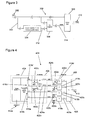
- FIG 4 illustrates further detail of an example of a frequency divider 400 according to an embodiment of the invention.
- the frequency divider 400 of Figure 4 is similar to that of Figure 3 , and corresponding features have been given similar reference numbers in the 400 series.
- the frequency divider 400 of Figure 4 is implemented to provide a non-integer frequency division factor of 4 1 ⁇ 4. (17/4). That is, the output signal 410 should provide a single output pulse for each 4.25 pulses of the input signalling. It will be recalled that each of the input signals has the same frequency and therefore it does not matter with which of the input signals the output is controlled in relation to.
- M LCM(K,n)/n
- the output signalling 410 should have rising edges at time instants 4.25, 8.5, 12.75 and 17 periods. Since the desired output events are evenly spaced throughout a single input period, a pre-alignment block 406 is placed between the counter 404 and the gating logic block 408 in order to delay one or more of the counter output events/signals by a fraction of a period. In this example, the counter 404 is driven by a single clock phase. The pre-alignment block 406 may be required because a counter 404 that is driven by a single clock phase cannot directly provide suitable 'enable' signalling for the gating logic 408 as will be described below.
- the timing of the whole system can be controlled so that the 'enable' outputs of the pre-alignment block 406 will always be active before a rising edge of the corresponding input phase signal 402 that is to be passed to the output signalling 410.
- the input phase signals 402 can be used to directly determine the timing of the edges of the output signalling, and delay and jitter caused by the counter and the pre-alignment block may not propagate though the system, or at least may be reduced when compared with the prior art.
- Four input signals 402a, 402b, 402c, 402d are provided as input oscillating signals to the frequency divider 400 and are labelled as “Input Phase 0", “Input Phase 1 ", “Input Phase 2” and “Input Phase 3" in Figure 4 .
- each input oscillating signal 402 is 90° phase-shifted in relation to its predecessor.
- non-integer division factors of 1.25, 1.5, 1.75, 2.25, 2.5, 2.75, etc. as well as integer division factors.
- the counter 404 has four programmable outputs 416a, 416b, 416c, 416d.
- the counter 404 comprises a programmable output selection logic module that sets the first counter output 416a high when the counter is at 4; sets the second counter output 416b high when the counter is at 8; sets the third counter output 416c high when the counter is at 12; and sets the fourth output 416d high when the counter is at 16.
- These are the integer values that are immediately before, but not equal to, the corresponding times at which a rising edge is required in the output signalling 410 (4.25, 8.5, 12.75, 17).
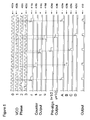
- the counter output signals 416a, 416b, 416c, 416d are shown in Figure 5 .
- the first counter output signal 416a is used to generate an output pulse of the frequency divider at an instance in time indicative of 4.25 periods from the point at which the counter 404 started counting.
- the output signalling 416a of the counter is provided directly as enable signalling to the gating logic 408. More particularly, the counter output signal 416a is provided as an input to an AND gate 418a of the gating logic 408.
- the second input oscillating signal 402b is also provided as an input to the AND gate 418a.
- the second input oscillating signal 402b is 90° phase shifted relative to the first oscillating signal 402a and therefore has a rising edge at a point in time corresponding to 0.25 x period after the rising edge of the first input oscillating signal 402a.
- Generating an enable signal in this way ensures that the output of the AND gate 418a will go high as soon as a rising edge is present on the second oscillating signal 402b after the enable signal 416a has been set. That is, the enable signal is set high at an instance in time before the rising edge of the second input oscillating signal 402b that is intended to be provided as an output pulse, but after the previous rising edge of the second input oscillating signal 402b so as not to provide an output pulse too early.
- the output of the AND gate 418a is referenced A 420a, and is also shown in the timing diagram of Figure 5 . It can be seen that the output A 420a of the AND gate 418a goes high for a single pulse at an instance in time representative of 4.25 time periods from the start of the first input oscillating signal 402a.
- the output A 420a of the AND gate 418a is provided as in input to an OR gate 426.
- the output of the OR gate 426 is the output signalling 410 of the frequency divider 400.
- Use of the OR gate 426 enables the output of the AND gate 418a, as well as the output signals of other AND gates 418 (as is described below) to be provided as the output signalling 410.
- Operation of a second AND gate 418b is very similar to operation of the first AND gate 418a.
- the second AND gate 418b receives the second counter output signal 416b as an enable signal, and processes this enable signal along with the third input oscillating signal 402c in order to provide an output pulse B 420b at an instance in time representative of 8.5 time periods after the start of the first oscillating input signal 402a.
- a third AND gate 420c is provided in order to generate an output pulse at an instance in time of 12.75 periods from the start of the first input oscillating signal 402a.
- the third counter output signal 416c is provided as an input to a delay flip-flop 422a.
- the clock input to the delay flip-flop 422a is configured to receive the third input oscillating signal 402c.
- the output of the delay flip-flop 422a is set high at half a period after the third counter output 416c is set. Effectively, the delay flip-flop 422a provides a 1 ⁇ 2 period time delay after the third counter output 416c is set.
- the output signal 424a of the delay flip-flop 422a is the enable signalling for the third AND gate 420c in the gating logic 408. Also provided as an input to the AND gate 420c is the fourth input oscillating signal 402d in order to generate the output pulse C 420c at the desired time.
- Operation of a fourth AND gate 418d is similar to the operation of the third AND gate 418c, and is configured to generate an output pulse at an instance in time representative of 17 time periods after the start of the first oscillating signal 402a.
- the enable signal 424b is generated using a delay flip-flop in order to ensure that the enable signal is set high before the pulse of the first oscillating signal 402a that is to be provided as the output 410 is received. This may be preferable to using an output of the counter to directly enable the AND gate 418d.
- the counter 404 may introduce a delay such that the enable signal 424b would not be high before the rising edge of the input oscillating signal that is to be passed to the output signal 410 is received. Such embodiments of the invention can remove and/or reduce the delay in passing an output pulse from the input oscillating signal 402a to the output signal 410.
- the programmable outputs of the counter 404, and how the delay flip flops 422 and logic gates 418, 426 are connected can be configured in any way, or replaced with any components that can perform the same function, in order to provide output signalling that is subject to the required non-integer frequency division factor.
- the output signalling 410 does not have a 50% duty cycle, but will consist of pulses with a length of 1 ⁇ 2 the clock period.
- the gating logic 408, or any other embodiment of an output signal selector block can contain components that are configured to adjust the duty cycle of the output signalling 410 as required. Examples of suitable components can include delay components, timer components, flip-flops, etc.
- the delay from a rising edge of an input phase signal to the rising edge of the output signalling can be identical for all phases, since the direct logic path from all input phase signals to the output can be identical.
- a feedback counter can be used that has a programmable modulus (M) and has programmable outputs (r, s, t and u).
- M programmable modulus
- r, s, t and u programmable outputs
- any division ratio K/n can be achieved by simply changing the modulus of the counter and re-programming the outputs in an appropriate fashion for a given the number of phases n.
- Advantages/features associated with one or more embodiments of the invention can include:
Landscapes
- Engineering & Computer Science (AREA)
- General Physics & Mathematics (AREA)
- Theoretical Computer Science (AREA)
- Physics & Mathematics (AREA)
- Mathematical Optimization (AREA)
- Mathematical Analysis (AREA)
- Computing Systems (AREA)
- Mathematical Physics (AREA)
- Pure & Applied Mathematics (AREA)
- General Engineering & Computer Science (AREA)
- Computational Mathematics (AREA)
- Stabilization Of Oscillater, Synchronisation, Frequency Synthesizers (AREA)
- Manipulation Of Pulses (AREA)
Priority Applications (3)
| Application Number | Priority Date | Filing Date | Title |
|---|---|---|---|
| EP09251896A EP2288031A1 (fr) | 2009-07-28 | 2009-07-28 | Diviseur de fréquence |
| CN2010102398513A CN101986566A (zh) | 2009-07-28 | 2010-07-26 | 分频器 |
| US12/843,078 US20110025382A1 (en) | 2009-07-28 | 2010-07-26 | Frequency divider |
Applications Claiming Priority (1)
| Application Number | Priority Date | Filing Date | Title |
|---|---|---|---|
| EP09251896A EP2288031A1 (fr) | 2009-07-28 | 2009-07-28 | Diviseur de fréquence |
Publications (1)
| Publication Number | Publication Date |
|---|---|
| EP2288031A1 true EP2288031A1 (fr) | 2011-02-23 |
Family
ID=41282513
Family Applications (1)
| Application Number | Title | Priority Date | Filing Date |
|---|---|---|---|
| EP09251896A Withdrawn EP2288031A1 (fr) | 2009-07-28 | 2009-07-28 | Diviseur de fréquence |
Country Status (3)
| Country | Link |
|---|---|
| US (1) | US20110025382A1 (fr) |
| EP (1) | EP2288031A1 (fr) |
| CN (1) | CN101986566A (fr) |
Families Citing this family (5)
| Publication number | Priority date | Publication date | Assignee | Title |
|---|---|---|---|---|
| US8723568B1 (en) * | 2013-12-20 | 2014-05-13 | Qualcomm Incorporated | Local oscillator signal generation using delay locked loops |
| CN103840767A (zh) * | 2014-03-10 | 2014-06-04 | 上海华虹宏力半导体制造有限公司 | 分频器、分频方法及射频系统 |
| CN103986457B (zh) * | 2014-05-20 | 2016-08-24 | 硅谷数模半导体(北京)有限公司 | 高速分频器 |
| JP2020202439A (ja) * | 2019-06-06 | 2020-12-17 | ソニーセミコンダクタソリューションズ株式会社 | 位相同期回路、電子装置、および、位相同期回路の制御方法 |
| US12266396B2 (en) * | 2023-03-31 | 2025-04-01 | Fujian Jinhua Integrated Circuit Co., Ltd. | Input data pre-alignment circuit capable of performing a first-in first-out signal alignment mechanism |
Citations (6)
| Publication number | Priority date | Publication date | Assignee | Title |
|---|---|---|---|---|
| US6114914A (en) * | 1999-05-19 | 2000-09-05 | Cypress Semiconductor Corp. | Fractional synthesis scheme for generating periodic signals |
| US6157694A (en) * | 1998-12-09 | 2000-12-05 | Lucent Technologies, Inc. | Fractional frequency divider |
| US20020027459A1 (en) | 1999-12-14 | 2002-03-07 | Siavash Fallahi | Frequency division/multiplication with jitter minimization |
| US6526374B1 (en) | 1999-12-13 | 2003-02-25 | Agere Systems Inc. | Fractional PLL employing a phase-selection feedback counter |
| US6542013B1 (en) | 2002-01-02 | 2003-04-01 | Intel Corporation | Fractional divisors for multiple-phase PLL systems |
| US20030198311A1 (en) * | 2002-04-19 | 2003-10-23 | Wireless Interface Technologies, Inc. | Fractional-N frequency synthesizer and method |
Family Cites Families (4)
| Publication number | Priority date | Publication date | Assignee | Title |
|---|---|---|---|---|
| US7145401B2 (en) * | 2005-01-21 | 2006-12-05 | Hewlett-Packard Development Company, L.P. | Method for the detection of an incorrect oscillator frequency and clock generation system |
| US7342465B2 (en) * | 2005-10-20 | 2008-03-11 | Honeywell International Inc. | Voltage-controlled oscillator with stable gain over a wide frequency range |
| WO2008141102A2 (fr) * | 2007-05-11 | 2008-11-20 | Skyworks Solutions, Inc. | Systemes et procedes permettant de fournir un signal d'horloge |
| US7551039B2 (en) * | 2007-10-19 | 2009-06-23 | Hewlett-Packard Development Company, L.P. | Phase adjustment in phase-locked loops using multiple oscillator signals |
-
2009
- 2009-07-28 EP EP09251896A patent/EP2288031A1/fr not_active Withdrawn
-
2010
- 2010-07-26 US US12/843,078 patent/US20110025382A1/en not_active Abandoned
- 2010-07-26 CN CN2010102398513A patent/CN101986566A/zh active Pending
Patent Citations (6)
| Publication number | Priority date | Publication date | Assignee | Title |
|---|---|---|---|---|
| US6157694A (en) * | 1998-12-09 | 2000-12-05 | Lucent Technologies, Inc. | Fractional frequency divider |
| US6114914A (en) * | 1999-05-19 | 2000-09-05 | Cypress Semiconductor Corp. | Fractional synthesis scheme for generating periodic signals |
| US6526374B1 (en) | 1999-12-13 | 2003-02-25 | Agere Systems Inc. | Fractional PLL employing a phase-selection feedback counter |
| US20020027459A1 (en) | 1999-12-14 | 2002-03-07 | Siavash Fallahi | Frequency division/multiplication with jitter minimization |
| US6542013B1 (en) | 2002-01-02 | 2003-04-01 | Intel Corporation | Fractional divisors for multiple-phase PLL systems |
| US20030198311A1 (en) * | 2002-04-19 | 2003-10-23 | Wireless Interface Technologies, Inc. | Fractional-N frequency synthesizer and method |
Also Published As
| Publication number | Publication date |
|---|---|
| US20110025382A1 (en) | 2011-02-03 |
| CN101986566A (zh) | 2011-03-16 |
Similar Documents
| Publication | Publication Date | Title |
|---|---|---|
| US7005900B1 (en) | Counter-based clock doubler circuits and methods with optional duty cycle correction and offset | |
| JP2577134B2 (ja) | プログラム可能な高速分割器 | |
| EP2629423B1 (fr) | Procédé entièrement numérique permettant de générer une division de sous-horloge et des ondes d'horloge | |
| US7956696B2 (en) | Techniques for generating fractional clock signals | |
| EP0596656A2 (fr) | Circuit programmable d'ajustement de décalage d'horloge | |
| US8891725B2 (en) | Frequency divider with improved linearity for a fractional-N synthesizer using a multi-modulus prescaler | |
| US6618462B1 (en) | Digital frequency divider | |
| CN201663588U (zh) | 一种实现多相位时钟分数分频的装置 | |
| CN110612667B (zh) | 频率产生器以及频率产生方法 | |
| EP2288031A1 (fr) | Diviseur de fréquence | |
| US8907704B2 (en) | Frequency synthesizer | |
| US6748408B1 (en) | Programmable non-integer fractional divider | |
| US20160308536A1 (en) | Multi-modulus divider with power-of-2 boundary condition support | |
| US20170373825A1 (en) | 1-16 & 1.5-7.5 Frequency Divider For Clock Synthesizer In Digital Systems | |
| US6556086B2 (en) | Fractional-N synthesizer and method of synchronization of the output phase | |
| US6906571B1 (en) | Counter-based phased clock generator circuits and methods | |
| US7881422B1 (en) | Circuits and methods for dividing frequency by an odd value | |
| US6526374B1 (en) | Fractional PLL employing a phase-selection feedback counter | |
| US6882190B2 (en) | Apparatus for frequency dividing a master clock signal by a non-integer | |
| US6316982B1 (en) | Digital clock with controllable phase skew | |
| EP4049370B1 (fr) | Circuit d'horloge numérique destiné à générer un signal d'horloge à multiplication de fréquence à rapport élevé | |
| TWI569582B (zh) | 時脈資料回復裝置、時脈資料回復方法及相位偵測器 | |
| US7496780B2 (en) | Reduction of data skew in parallel processing circuits | |
| JP2017512446A (ja) | 周波数シンセサイザ | |
| CN107547082B (zh) | 用于数字系统中时钟合成器的1-16和1.5-7.5分频器 |
Legal Events
| Date | Code | Title | Description |
|---|---|---|---|
| PUAI | Public reference made under article 153(3) epc to a published international application that has entered the european phase |
Free format text: ORIGINAL CODE: 0009012 |
|
| AK | Designated contracting states |
Kind code of ref document: A1 Designated state(s): AT BE BG CH CY CZ DE DK EE ES FI FR GB GR HR HU IE IS IT LI LT LU LV MC MK MT NL NO PL PT RO SE SI SK SM TR |
|
| AX | Request for extension of the european patent |
Extension state: AL BA RS |
|
| 17P | Request for examination filed |
Effective date: 20110823 |
|
| 17Q | First examination report despatched |
Effective date: 20110912 |
|
| STAA | Information on the status of an ep patent application or granted ep patent |
Free format text: STATUS: THE APPLICATION IS DEEMED TO BE WITHDRAWN |
|
| 18D | Application deemed to be withdrawn |
Effective date: 20120323 |