EP2288242A1 - Plaque multicouche à circuits imprimés micro-ondes ondulés et procédé - Google Patents
Plaque multicouche à circuits imprimés micro-ondes ondulés et procédé Download PDFInfo
- Publication number
- EP2288242A1 EP2288242A1 EP10251312A EP10251312A EP2288242A1 EP 2288242 A1 EP2288242 A1 EP 2288242A1 EP 10251312 A EP10251312 A EP 10251312A EP 10251312 A EP10251312 A EP 10251312A EP 2288242 A1 EP2288242 A1 EP 2288242A1
- Authority
- EP
- European Patent Office
- Prior art keywords
- flexible layer
- hole
- layer
- signal line
- flexible
- Prior art date
- Legal status (The legal status is an assumption and is not a legal conclusion. Google has not performed a legal analysis and makes no representation as to the accuracy of the status listed.)
- Withdrawn
Links
- 238000000034 method Methods 0.000 title claims abstract description 57
- 239000010410 layer Substances 0.000 claims abstract description 236
- 239000012790 adhesive layer Substances 0.000 claims abstract description 30
- 230000001070 adhesive effect Effects 0.000 claims description 10
- 239000000853 adhesive Substances 0.000 claims description 7
- 230000008878 coupling Effects 0.000 claims 4
- 238000010168 coupling process Methods 0.000 claims 4
- 238000005859 coupling reaction Methods 0.000 claims 4
- 230000008569 process Effects 0.000 description 37
- 238000004891 communication Methods 0.000 description 19
- 239000004020 conductor Substances 0.000 description 18
- 230000005540 biological transmission Effects 0.000 description 9
- 238000013461 design Methods 0.000 description 4
- 230000037361 pathway Effects 0.000 description 4
- 108091092878 Microsatellite Proteins 0.000 description 3
- 230000002730 additional effect Effects 0.000 description 2
- 239000002313 adhesive film Substances 0.000 description 2
- 230000006835 compression Effects 0.000 description 2
- 238000007906 compression Methods 0.000 description 2
- 238000010276 construction Methods 0.000 description 2
- 230000004927 fusion Effects 0.000 description 2
- 238000003780 insertion Methods 0.000 description 2
- 230000037431 insertion Effects 0.000 description 2
- 238000004519 manufacturing process Methods 0.000 description 2
- 239000000123 paper Substances 0.000 description 2
- 238000011160 research Methods 0.000 description 2
- 239000013585 weight reducing agent Substances 0.000 description 2
- HHXNVASVVVNNDG-UHFFFAOYSA-N 1,2,3,4,5-pentachloro-6-(2,3,6-trichlorophenyl)benzene Chemical compound ClC1=CC=C(Cl)C(C=2C(=C(Cl)C(Cl)=C(Cl)C=2Cl)Cl)=C1Cl HHXNVASVVVNNDG-UHFFFAOYSA-N 0.000 description 1
- 238000003491 array Methods 0.000 description 1
- 230000000712 assembly Effects 0.000 description 1
- 238000000429 assembly Methods 0.000 description 1
- 238000005452 bending Methods 0.000 description 1
- 239000011096 corrugated fiberboard Substances 0.000 description 1
- 230000007123 defense Effects 0.000 description 1
- 238000011161 development Methods 0.000 description 1
- 238000009434 installation Methods 0.000 description 1
- 239000012212 insulator Substances 0.000 description 1
- 239000000463 material Substances 0.000 description 1
- 229910000679 solder Inorganic materials 0.000 description 1
- 239000007787 solid Substances 0.000 description 1
- 125000006850 spacer group Chemical group 0.000 description 1
- 230000007704 transition Effects 0.000 description 1
Images




Classifications
-
- H—ELECTRICITY
- H05—ELECTRIC TECHNIQUES NOT OTHERWISE PROVIDED FOR
- H05K—PRINTED CIRCUITS; CASINGS OR CONSTRUCTIONAL DETAILS OF ELECTRIC APPARATUS; MANUFACTURE OF ASSEMBLAGES OF ELECTRICAL COMPONENTS
- H05K1/00—Printed circuits
- H05K1/02—Details
- H05K1/0213—Electrical arrangements not otherwise provided for
- H05K1/0237—High frequency adaptations
- H05K1/024—Dielectric details, e.g. changing the dielectric material around a transmission line
-
- H—ELECTRICITY
- H05—ELECTRIC TECHNIQUES NOT OTHERWISE PROVIDED FOR
- H05K—PRINTED CIRCUITS; CASINGS OR CONSTRUCTIONAL DETAILS OF ELECTRIC APPARATUS; MANUFACTURE OF ASSEMBLAGES OF ELECTRICAL COMPONENTS
- H05K1/00—Printed circuits
- H05K1/02—Details
- H05K1/0277—Bendability or stretchability details
- H05K1/028—Bending or folding regions of flexible printed circuits
-
- H—ELECTRICITY
- H05—ELECTRIC TECHNIQUES NOT OTHERWISE PROVIDED FOR
- H05K—PRINTED CIRCUITS; CASINGS OR CONSTRUCTIONAL DETAILS OF ELECTRIC APPARATUS; MANUFACTURE OF ASSEMBLAGES OF ELECTRICAL COMPONENTS
- H05K1/00—Printed circuits
- H05K1/02—Details
- H05K1/14—Structural association of two or more printed circuits
- H05K1/147—Structural association of two or more printed circuits at least one of the printed circuits being bent or folded, e.g. by using a flexible printed circuit
-
- H—ELECTRICITY
- H05—ELECTRIC TECHNIQUES NOT OTHERWISE PROVIDED FOR
- H05K—PRINTED CIRCUITS; CASINGS OR CONSTRUCTIONAL DETAILS OF ELECTRIC APPARATUS; MANUFACTURE OF ASSEMBLAGES OF ELECTRICAL COMPONENTS
- H05K3/00—Apparatus or processes for manufacturing printed circuits
- H05K3/36—Assembling printed circuits with other printed circuits
- H05K3/361—Assembling flexible printed circuits with other printed circuits
-
- H—ELECTRICITY
- H05—ELECTRIC TECHNIQUES NOT OTHERWISE PROVIDED FOR
- H05K—PRINTED CIRCUITS; CASINGS OR CONSTRUCTIONAL DETAILS OF ELECTRIC APPARATUS; MANUFACTURE OF ASSEMBLAGES OF ELECTRICAL COMPONENTS
- H05K1/00—Printed circuits
- H05K1/02—Details
- H05K1/14—Structural association of two or more printed circuits
- H05K1/144—Stacked arrangements of planar printed circuit boards
-
- H—ELECTRICITY
- H05—ELECTRIC TECHNIQUES NOT OTHERWISE PROVIDED FOR
- H05K—PRINTED CIRCUITS; CASINGS OR CONSTRUCTIONAL DETAILS OF ELECTRIC APPARATUS; MANUFACTURE OF ASSEMBLAGES OF ELECTRICAL COMPONENTS
- H05K2201/00—Indexing scheme relating to printed circuits covered by H05K1/00
- H05K2201/05—Flexible printed circuits [FPCs]
- H05K2201/055—Folded back on itself
-
- H—ELECTRICITY
- H05—ELECTRIC TECHNIQUES NOT OTHERWISE PROVIDED FOR
- H05K—PRINTED CIRCUITS; CASINGS OR CONSTRUCTIONAL DETAILS OF ELECTRIC APPARATUS; MANUFACTURE OF ASSEMBLAGES OF ELECTRICAL COMPONENTS
- H05K2201/00—Indexing scheme relating to printed circuits covered by H05K1/00
- H05K2201/05—Flexible printed circuits [FPCs]
- H05K2201/058—Direct connection between two or more FPCs or between flexible parts of rigid PCBs
-
- H—ELECTRICITY
- H05—ELECTRIC TECHNIQUES NOT OTHERWISE PROVIDED FOR
- H05K—PRINTED CIRCUITS; CASINGS OR CONSTRUCTIONAL DETAILS OF ELECTRIC APPARATUS; MANUFACTURE OF ASSEMBLAGES OF ELECTRICAL COMPONENTS
- H05K2201/00—Indexing scheme relating to printed circuits covered by H05K1/00
- H05K2201/09—Shape and layout
- H05K2201/09009—Substrate related
- H05K2201/09109—Locally detached layers, e.g. in multilayer
-
- H—ELECTRICITY
- H05—ELECTRIC TECHNIQUES NOT OTHERWISE PROVIDED FOR
- H05K—PRINTED CIRCUITS; CASINGS OR CONSTRUCTIONAL DETAILS OF ELECTRIC APPARATUS; MANUFACTURE OF ASSEMBLAGES OF ELECTRICAL COMPONENTS
- H05K2201/00—Indexing scheme relating to printed circuits covered by H05K1/00
- H05K2201/09—Shape and layout
- H05K2201/09209—Shape and layout details of conductors
- H05K2201/0929—Conductive planes
- H05K2201/09318—Core having one signal plane and one power plane
-
- H—ELECTRICITY
- H05—ELECTRIC TECHNIQUES NOT OTHERWISE PROVIDED FOR
- H05K—PRINTED CIRCUITS; CASINGS OR CONSTRUCTIONAL DETAILS OF ELECTRIC APPARATUS; MANUFACTURE OF ASSEMBLAGES OF ELECTRICAL COMPONENTS
- H05K2201/00—Indexing scheme relating to printed circuits covered by H05K1/00
- H05K2201/10—Details of components or other objects attached to or integrated in a printed circuit board
- H05K2201/10227—Other objects, e.g. metallic pieces
- H05K2201/10378—Interposers
-
- H—ELECTRICITY
- H05—ELECTRIC TECHNIQUES NOT OTHERWISE PROVIDED FOR
- H05K—PRINTED CIRCUITS; CASINGS OR CONSTRUCTIONAL DETAILS OF ELECTRIC APPARATUS; MANUFACTURE OF ASSEMBLAGES OF ELECTRICAL COMPONENTS
- H05K2203/00—Indexing scheme relating to apparatus or processes for manufacturing printed circuits covered by H05K3/00
- H05K2203/06—Lamination
- H05K2203/063—Lamination of preperforated insulating layer
-
- H—ELECTRICITY
- H05—ELECTRIC TECHNIQUES NOT OTHERWISE PROVIDED FOR
- H05K—PRINTED CIRCUITS; CASINGS OR CONSTRUCTIONAL DETAILS OF ELECTRIC APPARATUS; MANUFACTURE OF ASSEMBLAGES OF ELECTRICAL COMPONENTS
- H05K3/00—Apparatus or processes for manufacturing printed circuits
- H05K3/40—Forming printed elements for providing electric connections to or between printed circuits
- H05K3/4038—Through-connections; Vertical interconnect access [VIA] connections
- H05K3/4053—Through-connections; Vertical interconnect access [VIA] connections by thick-film techniques
- H05K3/4069—Through-connections; Vertical interconnect access [VIA] connections by thick-film techniques for via connections in organic insulating substrates
-
- H—ELECTRICITY
- H05—ELECTRIC TECHNIQUES NOT OTHERWISE PROVIDED FOR
- H05K—PRINTED CIRCUITS; CASINGS OR CONSTRUCTIONAL DETAILS OF ELECTRIC APPARATUS; MANUFACTURE OF ASSEMBLAGES OF ELECTRICAL COMPONENTS
- H05K3/00—Apparatus or processes for manufacturing printed circuits
- H05K3/46—Manufacturing multilayer circuits
- H05K3/4611—Manufacturing multilayer circuits by laminating two or more circuit boards
- H05K3/4614—Manufacturing multilayer circuits by laminating two or more circuit boards the electrical connections between the circuit boards being made during lamination
-
- H—ELECTRICITY
- H05—ELECTRIC TECHNIQUES NOT OTHERWISE PROVIDED FOR
- H05K—PRINTED CIRCUITS; CASINGS OR CONSTRUCTIONAL DETAILS OF ELECTRIC APPARATUS; MANUFACTURE OF ASSEMBLAGES OF ELECTRICAL COMPONENTS
- H05K3/00—Apparatus or processes for manufacturing printed circuits
- H05K3/46—Manufacturing multilayer circuits
- H05K3/4611—Manufacturing multilayer circuits by laminating two or more circuit boards
- H05K3/4626—Manufacturing multilayer circuits by laminating two or more circuit boards characterised by the insulating layers or materials
- H05K3/4635—Manufacturing multilayer circuits by laminating two or more circuit boards characterised by the insulating layers or materials laminating flexible circuit boards using additional insulating adhesive materials between the boards
-
- Y—GENERAL TAGGING OF NEW TECHNOLOGICAL DEVELOPMENTS; GENERAL TAGGING OF CROSS-SECTIONAL TECHNOLOGIES SPANNING OVER SEVERAL SECTIONS OF THE IPC; TECHNICAL SUBJECTS COVERED BY FORMER USPC CROSS-REFERENCE ART COLLECTIONS [XRACs] AND DIGESTS
- Y10—TECHNICAL SUBJECTS COVERED BY FORMER USPC
- Y10T—TECHNICAL SUBJECTS COVERED BY FORMER US CLASSIFICATION
- Y10T29/00—Metal working
- Y10T29/49—Method of mechanical manufacture
- Y10T29/49002—Electrical device making
- Y10T29/49117—Conductor or circuit manufacturing
- Y10T29/49124—On flat or curved insulated base, e.g., printed circuit, etc.
- Y10T29/49126—Assembling bases
-
- Y—GENERAL TAGGING OF NEW TECHNOLOGICAL DEVELOPMENTS; GENERAL TAGGING OF CROSS-SECTIONAL TECHNOLOGIES SPANNING OVER SEVERAL SECTIONS OF THE IPC; TECHNICAL SUBJECTS COVERED BY FORMER USPC CROSS-REFERENCE ART COLLECTIONS [XRACs] AND DIGESTS
- Y10—TECHNICAL SUBJECTS COVERED BY FORMER USPC
- Y10T—TECHNICAL SUBJECTS COVERED BY FORMER US CLASSIFICATION
- Y10T29/00—Metal working
- Y10T29/49—Method of mechanical manufacture
- Y10T29/49002—Electrical device making
- Y10T29/49117—Conductor or circuit manufacturing
- Y10T29/49124—On flat or curved insulated base, e.g., printed circuit, etc.
- Y10T29/49155—Manufacturing circuit on or in base
Definitions
- FIG. 3 is a perspective view of the two layer corrugated printed circuit board of FIG. 2 .
- FIG. 8 is a top view of a portion of the interconnect of FIG. 7 including three lines of a microstrip transmission line in accordance with one embodiment of the invention.
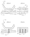
- FIG. 11 is an exploded cross sectional view of the interconnect of FIG. 10 taken along section A-A.
- FIG. 12 is a cross sectional view of the interconnect of FIG. 10 illustrating a through hole extending through the flat flex layer and the adhesive layer to a conductor pad positioned on the folded flex layer of the interconnect.
- Embodiments of the corrugated PCBs described herein incorporate this same principle when they include arches in the corrugated medium. These arches are known as flutes and when anchored to a linerboard with an adhesive, they resist bending and pressure from all directions.
- Corrugated fiberboard, or combined board has two main components: the linerboard and the medium. Both are made of a special kind of heavy paper called container board for cardboard applications (e.g., boxes). Linerboard is the flat facing that adheres to the medium. The medium is the wavy, fluted paper in between the liners.
- the corrugation manufacturing processes are most commonly used to make boxes having one layer of fluting between two smooth sheets.
- the arches form rigid columns, capable of supporting a great deal of weight.
- the space in between the flutes acts as a cushion to protect the container's contents.
- the flutes also serve as an insulator, providing some product protection from sudden temperature changes.
- the vertical liner board provides more strength and protects the flutes from damage. Flutes come in several standard shapes or flute profiles.
- FIG. 7 is a close up view of an interconnect 300 between a folded flex layer 310 and a flat flex layer 312 of a corrugated printed circuit board in accordance with one embodiment of the invention.
- the interconnect 300 further includes a dielectric adhesive layer 311 or spacer disposed between the folded flex layer 310 and the flat flex layer 312.
- An RF communication signal 313 passes along the flat flex layer 312 toward and through the adhesive layer 311 and then along the folded flex layer 310.
- the flat flex layer 312 is configured as a microstrip transmission line or microstripline for passing the RF communication signal 313.
- the RF communication signal 313 passes along the bottom of the flat layer 312, via signal conductor 315, from right to left, transitions to the folded layer 310 via the interconnect and continues along a bottom of the folded layer 310, via signal conductor 319.
- the RF communication signal 313 can follow other suitable paths along the flat and folded layers.
- the dielectric adhesive layer can have a dielectric constant of 3.5. In other embodiments, the dielectric adhesive layer can have other suitable dielectric constant values.
- the folded flex layer and the flat flex layer are configured as microstripline transmission lines. In other embodiments, the folded flex layer and the flat flex layer can be configured to support other suitable types of transmission lines.
- an RF communication signal can pass along the flat flex layer 412 toward and through the adhesive layer 411 and then along the folded flex layer 410 or vice versa.
- the folded flex layer 410 is configured as a microstrip transmission line or microstripline for passing the RF communication signal.
- the flat layer 410 has a signal conductor 419, or microstripline, disposed along a bottom surface of the folded layer 410 and a groundplane conductor 421 disposed along a top surface of the flat layer 410.
- the process first designs and fabricates (501) a bottom flexible circuit, or flex circuit, with a hole and an annular ring at preselected attachment locations on a top surface of the bottom flex circuit.
- the process also designs and fabricates (502) a top flexible circuit with conductive pads at preselected attachment locations, that correspond to the attachment locations of the bottom flex circuit, on a bottom surface of the top flex circuit.
- the process can mechanically attach the flex circuits using multiple sub-processes.
- the process aligns (506) and fusion bonds (507) the flex circuits.
- the aligning can include aligning the top and bottom flex circuits so that the holes are in line with the pads.
- a second sub-process (dashed arrow path (2)), the process dispenses (505) a non-conductive paste on the top and/or bottom flex circuits. The process then aligns (506) the flex circuits and bonds (508) the common flat areas of the flex circuits together using heat and pressure.
Landscapes
- Engineering & Computer Science (AREA)
- Microelectronics & Electronic Packaging (AREA)
- Manufacturing & Machinery (AREA)
- Structure Of Printed Boards (AREA)
- Combinations Of Printed Boards (AREA)
- Printing Elements For Providing Electric Connections Between Printed Circuits (AREA)
Applications Claiming Priority (1)
| Application Number | Priority Date | Filing Date | Title |
|---|---|---|---|
| US12/534,077 US20110024160A1 (en) | 2009-07-31 | 2009-07-31 | Multi-layer microwave corrugated printed circuit board and method |
Publications (1)
| Publication Number | Publication Date |
|---|---|
| EP2288242A1 true EP2288242A1 (fr) | 2011-02-23 |
Family
ID=43037070
Family Applications (1)
| Application Number | Title | Priority Date | Filing Date |
|---|---|---|---|
| EP10251312A Withdrawn EP2288242A1 (fr) | 2009-07-31 | 2010-07-23 | Plaque multicouche à circuits imprimés micro-ondes ondulés et procédé |
Country Status (5)
| Country | Link |
|---|---|
| US (2) | US20110024160A1 (fr) |
| EP (1) | EP2288242A1 (fr) |
| JP (1) | JP5221606B2 (fr) |
| KR (1) | KR101139581B1 (fr) |
| IL (1) | IL206729A (fr) |
Cited By (7)
| Publication number | Priority date | Publication date | Assignee | Title |
|---|---|---|---|---|
| EP2323467A1 (fr) * | 2009-11-17 | 2011-05-18 | Raytheon Company | Procédé de fabrication d'une structure de rayonnement d'antenne à forme d'origami |
| US8043464B2 (en) | 2009-11-17 | 2011-10-25 | Raytheon Company | Systems and methods for assembling lightweight RF antenna structures |
| US8362856B2 (en) | 2009-11-17 | 2013-01-29 | Raytheon Company | RF transition with 3-dimensional molded RF structure |
| US9072164B2 (en) | 2009-11-17 | 2015-06-30 | Raytheon Company | Process for fabricating a three dimensional molded feed structure |
| US9491854B2 (en) | 2009-07-31 | 2016-11-08 | Raytheon Company | Multi-layer microwave corrugated printed circuit board and method |
| CN109727848A (zh) * | 2018-12-29 | 2019-05-07 | 长江存储科技有限责任公司 | 一种三维存储器的制造方法 |
| EP3579669A2 (fr) * | 2018-06-07 | 2019-12-11 | AT & S Austria Technologie & Systemtechnik Aktiengesellschaft | Couche déformée pour une connexion électrique courte entre des structures de dispositif électrique |
Families Citing this family (12)
| Publication number | Priority date | Publication date | Assignee | Title |
|---|---|---|---|---|
| USD661265S1 (en) * | 2010-05-19 | 2012-06-05 | Nippon Mektron, Ltd. | Flexible printed circuit board |
| USD669045S1 (en) * | 2010-05-19 | 2012-10-16 | Nippon Mektron, Ltd. | Flexible printed circuit board |
| USD669046S1 (en) * | 2010-05-19 | 2012-10-16 | Nippon Mektron, Ltd | Flexible printed circuit board |
| USD656111S1 (en) * | 2010-05-19 | 2012-03-20 | Nippon Mektron, Ltd. | Flexible printed circuit board |
| USD687397S1 (en) * | 2010-05-19 | 2013-08-06 | Nippon Mektron, Ltd. | Flexible printed circuit board |
| USD656112S1 (en) * | 2010-05-19 | 2012-03-20 | Nippon Mektron, Ltd. | Flexible printed circuit board |
| US20130224405A1 (en) * | 2012-02-23 | 2013-08-29 | Lockheed Martin Corporation | Electromagnetic meta-materials |
| WO2014125852A1 (fr) * | 2013-02-14 | 2014-08-21 | 株式会社村田製作所 | Substrat de circuit et son procédé de production |
| US20140264938A1 (en) * | 2013-03-14 | 2014-09-18 | Douglas R. Hackler, Sr. | Flexible Interconnect |
| JP1588722S (fr) * | 2017-02-15 | 2017-10-23 | ||
| KR102679250B1 (ko) * | 2018-09-12 | 2024-06-28 | 엘지이노텍 주식회사 | 연성 회로기판 및 이를 포함하는 칩 패키지, 및 이를 포함하는 전자 디바이스 |
| WO2022060964A1 (fr) * | 2020-09-16 | 2022-03-24 | Google Llc | Interconnexion de carte de circuit imprimé flexible à jonction de chevauchement |
Citations (6)
| Publication number | Priority date | Publication date | Assignee | Title |
|---|---|---|---|---|
| US3004229A (en) * | 1959-02-24 | 1961-10-10 | Sanders Associates Inc | High frequency transmission line |
| GB2064233A (en) * | 1979-11-14 | 1981-06-10 | Hitachi Ltd | Liquid crystal display device |
| JPH0851279A (ja) * | 1994-08-05 | 1996-02-20 | Yazaki Corp | 配線板の接続方法 |
| JPH09281520A (ja) * | 1996-04-10 | 1997-10-31 | Seiko Epson Corp | 回路基板の接続方法、液晶表示装置、電子機器 |
| FR2871336A1 (fr) * | 2004-06-02 | 2005-12-09 | Bree Ind Soc Par Actions Simpl | Circuit imprime flex-rigide par collage |
| US7525498B2 (en) | 2006-10-11 | 2009-04-28 | Raytheon Company | Antenna array |
Family Cites Families (45)
| Publication number | Priority date | Publication date | Assignee | Title |
|---|---|---|---|---|
| US231226A (en) * | 1880-08-17 | Telephone-transmitter | ||
| US131451A (en) * | 1872-09-17 | Improvement in dish-washers | ||
| US165296A (en) * | 1875-07-06 | Improvement in wash-stands | ||
| US723548A (en) * | 1900-03-21 | 1903-03-24 | Holyoke Machine Company | Founder's molding-machine. |
| US4126508A (en) * | 1976-09-13 | 1978-11-21 | Boise Cascade Corporation | Apparatus for forming multi-flute-layer corrugated board |
| US4853660A (en) * | 1988-06-30 | 1989-08-01 | Raytheon Company | Integratable microwave devices based on ferromagnetic films disposed on dielectric substrates |
| US5097101A (en) | 1991-02-05 | 1992-03-17 | Tektronix, Inc. | Method of forming a conductive contact bump on a flexible substrate and a flexible substrate |
| US5343616B1 (en) | 1992-02-14 | 1998-12-29 | Rock Ltd | Method of making high density self-aligning conductive networks and contact clusters |
| US5262590A (en) * | 1992-04-27 | 1993-11-16 | Sheldahl, Inc. | Impedance controlled flexible circuits with fold-over shields |
| US5408240A (en) | 1993-12-23 | 1995-04-18 | Hughes Aircraft Company | Suspended stripline RF feed with orthogonal coaxial transitions and plastic housing |
| US5633615A (en) | 1995-12-26 | 1997-05-27 | Hughes Electronics | Vertical right angle solderless interconnects from suspended stripline to three-wire lines on MIC substrates |
| JP3574308B2 (ja) * | 1997-09-02 | 2004-10-06 | アルプス電気株式会社 | 積層基板およびこれを用いたデータ入力装置 |
| US6018326A (en) | 1997-09-29 | 2000-01-25 | Ericsson Inc. | Antennas with integrated windings |
| US6061245A (en) * | 1998-01-22 | 2000-05-09 | International Business Machines Corporation | Free standing, three dimensional, multi-chip, carrier package with air flow baffle |
| JPH11284332A (ja) * | 1998-03-30 | 1999-10-15 | Jsr Corp | 配線基板積層用接着性シートおよびその製造方法並びに積層型コネクターおよびその製造方法 |
| JPH11330645A (ja) * | 1998-05-19 | 1999-11-30 | Matsushita Electric Ind Co Ltd | 表層及び内層の銅箔面積を増大したプリント基板 |
| JP2000332419A (ja) * | 1999-05-24 | 2000-11-30 | Hitachi Ltd | 多層プリント基板および液晶表示装置 |
| JP3654095B2 (ja) * | 1999-11-05 | 2005-06-02 | 三菱電機株式会社 | 高周波プリント配線板及びその製造方法 |
| JP2001189609A (ja) * | 1999-12-28 | 2001-07-10 | Mitsubishi Electric Corp | マイクロストリップ線路接続体 |
| US6366185B1 (en) | 2000-01-12 | 2002-04-02 | Raytheon Company | Vertical interconnect between coaxial or GCPW circuits and airline via compressible center conductors |
| JP3495305B2 (ja) * | 2000-02-02 | 2004-02-09 | Necエレクトロニクス株式会社 | 半導体装置及び半導体モジュール |
| US6444921B1 (en) * | 2000-02-03 | 2002-09-03 | Fujitsu Limited | Reduced stress and zero stress interposers for integrated-circuit chips, multichip substrates, and the like |
| US6871396B2 (en) * | 2000-02-09 | 2005-03-29 | Matsushita Electric Industrial Co., Ltd. | Transfer material for wiring substrate |
| US7298331B2 (en) | 2000-03-13 | 2007-11-20 | Rcd Technology, Inc. | Method for forming radio frequency antenna |
| US6696163B2 (en) * | 2000-07-18 | 2004-02-24 | 3M Innovative Properties Company | Liquid crystal polymers for flexible circuits |
| JP2003347503A (ja) * | 2002-05-30 | 2003-12-05 | Hitachi Ltd | 半導体装置及びその製造方法並びに半導体実装方法 |
| JP2004221345A (ja) * | 2003-01-15 | 2004-08-05 | Sumitomo Electric Ind Ltd | フレキシブル基板およびその接続方法 |
| US6992629B2 (en) * | 2003-09-03 | 2006-01-31 | Raytheon Company | Embedded RF vertical interconnect for flexible conformal antenna |
| JP4253280B2 (ja) | 2003-12-05 | 2009-04-08 | 三井金属鉱業株式会社 | プリント配線基板の製造方法 |
| US7057563B2 (en) * | 2004-05-28 | 2006-06-06 | Raytheon Company | Radiator structures |
| US7109943B2 (en) * | 2004-10-21 | 2006-09-19 | The Boeing Company | Structurally integrated antenna aperture and fabrication method |
| DE602006006063D1 (de) * | 2005-07-29 | 2009-05-14 | Tyco Electronics Corp | Schutzvorrichtung für einen schaltkreis mit wärmegekoppeltem mov-überspannungselement und pptc-überstromelement |
| US7645942B2 (en) | 2005-12-09 | 2010-01-12 | Xerox Corporation | Electrical interconnect with maximized electrical contact |
| US7463198B2 (en) * | 2005-12-16 | 2008-12-09 | Applied Radar Inc. | Non-woven textile microwave antennas and components |
| JP2007221077A (ja) * | 2006-02-20 | 2007-08-30 | Fujikura Ltd | プリント配線板の接続構造および接続方法 |
| US20090165296A1 (en) | 2006-04-04 | 2009-07-02 | Yoash Carmi | Patterns of conductive objects on a substrate and method of producing thereof |
| US7992293B2 (en) | 2006-04-04 | 2011-08-09 | Hanita Coatings R.C.A. Ltd | Method of manufacturing a patterned conductive layer |
| US7645941B2 (en) * | 2006-05-02 | 2010-01-12 | Multi-Fineline Electronix, Inc. | Shielded flexible circuits and methods for manufacturing same |
| US8059049B2 (en) | 2006-10-11 | 2011-11-15 | Raytheon Company | Dual band active array antenna |
| US8026863B2 (en) | 2006-10-11 | 2011-09-27 | Raytheon Company | Transmit/receive module communication and control architechture for active array |
| US20110024160A1 (en) | 2009-07-31 | 2011-02-03 | Clifton Quan | Multi-layer microwave corrugated printed circuit board and method |
| US8043464B2 (en) * | 2009-11-17 | 2011-10-25 | Raytheon Company | Systems and methods for assembling lightweight RF antenna structures |
| US8127432B2 (en) | 2009-11-17 | 2012-03-06 | Raytheon Company | Process for fabricating an origami formed antenna radiating structure |
| US8362856B2 (en) * | 2009-11-17 | 2013-01-29 | Raytheon Company | RF transition with 3-dimensional molded RF structure |
| US9072164B2 (en) * | 2009-11-17 | 2015-06-30 | Raytheon Company | Process for fabricating a three dimensional molded feed structure |
-
2009
- 2009-07-31 US US12/534,077 patent/US20110024160A1/en not_active Abandoned
-
2010
- 2010-06-30 IL IL206729A patent/IL206729A/en active IP Right Grant
- 2010-07-23 EP EP10251312A patent/EP2288242A1/fr not_active Withdrawn
- 2010-07-30 JP JP2010171363A patent/JP5221606B2/ja active Active
- 2010-07-30 KR KR1020100074338A patent/KR101139581B1/ko active Active
-
2013
- 2013-04-18 US US13/865,730 patent/US9491854B2/en active Active
Patent Citations (6)
| Publication number | Priority date | Publication date | Assignee | Title |
|---|---|---|---|---|
| US3004229A (en) * | 1959-02-24 | 1961-10-10 | Sanders Associates Inc | High frequency transmission line |
| GB2064233A (en) * | 1979-11-14 | 1981-06-10 | Hitachi Ltd | Liquid crystal display device |
| JPH0851279A (ja) * | 1994-08-05 | 1996-02-20 | Yazaki Corp | 配線板の接続方法 |
| JPH09281520A (ja) * | 1996-04-10 | 1997-10-31 | Seiko Epson Corp | 回路基板の接続方法、液晶表示装置、電子機器 |
| FR2871336A1 (fr) * | 2004-06-02 | 2005-12-09 | Bree Ind Soc Par Actions Simpl | Circuit imprime flex-rigide par collage |
| US7525498B2 (en) | 2006-10-11 | 2009-04-28 | Raytheon Company | Antenna array |
Cited By (12)
| Publication number | Priority date | Publication date | Assignee | Title |
|---|---|---|---|---|
| US9491854B2 (en) | 2009-07-31 | 2016-11-08 | Raytheon Company | Multi-layer microwave corrugated printed circuit board and method |
| EP2323467A1 (fr) * | 2009-11-17 | 2011-05-18 | Raytheon Company | Procédé de fabrication d'une structure de rayonnement d'antenne à forme d'origami |
| US8043464B2 (en) | 2009-11-17 | 2011-10-25 | Raytheon Company | Systems and methods for assembling lightweight RF antenna structures |
| US8127432B2 (en) | 2009-11-17 | 2012-03-06 | Raytheon Company | Process for fabricating an origami formed antenna radiating structure |
| US8362856B2 (en) | 2009-11-17 | 2013-01-29 | Raytheon Company | RF transition with 3-dimensional molded RF structure |
| US8453314B2 (en) | 2009-11-17 | 2013-06-04 | Raytheon Company | Process for forming channels in a flexible circuit substrate using an elongated wedge and a channel shaped receptacle |
| US9072164B2 (en) | 2009-11-17 | 2015-06-30 | Raytheon Company | Process for fabricating a three dimensional molded feed structure |
| EP3579669A2 (fr) * | 2018-06-07 | 2019-12-11 | AT & S Austria Technologie & Systemtechnik Aktiengesellschaft | Couche déformée pour une connexion électrique courte entre des structures de dispositif électrique |
| CN110581417A (zh) * | 2018-06-07 | 2019-12-17 | 奥特斯奥地利科技与系统技术有限公司 | 用于电气装置结构之间的短电气连接的变形层 |
| EP3579669A3 (fr) * | 2018-06-07 | 2020-04-29 | AT & S Austria Technologie & Systemtechnik Aktiengesellschaft | Couche déformée pour une connexion électrique courte entre des structures de dispositif électrique |
| EP4608077A3 (fr) * | 2018-06-07 | 2025-11-19 | AT & S Austria Technologie & Systemtechnik Aktiengesellschaft | Couche déformée pour connexion électrique courte entre des structures d'un dispositif électrique |
| CN109727848A (zh) * | 2018-12-29 | 2019-05-07 | 长江存储科技有限责任公司 | 一种三维存储器的制造方法 |
Also Published As
| Publication number | Publication date |
|---|---|
| US20130319732A1 (en) | 2013-12-05 |
| JP5221606B2 (ja) | 2013-06-26 |
| KR101139581B1 (ko) | 2012-04-27 |
| IL206729A (en) | 2015-08-31 |
| US9491854B2 (en) | 2016-11-08 |
| IL206729A0 (en) | 2010-12-30 |
| US20110024160A1 (en) | 2011-02-03 |
| KR20110013333A (ko) | 2011-02-09 |
| JP2011035401A (ja) | 2011-02-17 |
Similar Documents
| Publication | Publication Date | Title |
|---|---|---|
| US9491854B2 (en) | Multi-layer microwave corrugated printed circuit board and method | |
| US7489524B2 (en) | Assembly including vertical and horizontal joined circuit panels | |
| JP6593444B2 (ja) | アンテナ一体型通信モジュール | |
| CN103731984B (zh) | 具有阻抗控制结构的软硬结合电路板 | |
| TWI463736B (zh) | 具有整合孔隙耦合貼片天線之射頻積體電路封裝 | |
| JP4463102B2 (ja) | 多層ストリップライン・アセンブリの相互接続及び相互接続方法 | |
| CN102007822B (zh) | 移除了信号传输线周围的粘结片的印刷电路板 | |
| US20060043562A1 (en) | Circuit device and manufacture method for circuit device | |
| CN105050313B (zh) | 多层基板和制造多层基板的方法 | |
| US20100163282A1 (en) | Printed wiring board, method for manufacturing printed wiring board, and electric device | |
| CN102137541A (zh) | 刚挠性电路板及其制造方法 | |
| EP3563447B1 (fr) | Système d'interconnexion pour circuit radiofréquence multicouche et procédé de fabrication | |
| US20110115578A1 (en) | Rf transition with 3-dimensional molded rf structure | |
| US10342125B2 (en) | Multilayer substrate | |
| EP2284887A2 (fr) | Module constitué de dispositifs semi-conducteurs et procédé de fabrication du module | |
| US8547280B2 (en) | Systems and methods for exciting long slot radiators of an RF antenna | |
| EP1951009B1 (fr) | Carte de circuit imprimé | |
| US8076591B2 (en) | Circuit boards | |
| US20120099285A1 (en) | Laminated substrate with coils | |
| JP6558514B2 (ja) | 電子機器 | |
| US8841561B1 (en) | High performance PCB | |
| JP2006108741A (ja) | 高周波電力分配合成器 | |
| JP6569826B2 (ja) | アンテナモジュール | |
| JP2021078003A (ja) | 無線モジュール | |
| CN120456457A (zh) | 双侧叠板方法 |
Legal Events
| Date | Code | Title | Description |
|---|---|---|---|
| PUAI | Public reference made under article 153(3) epc to a published international application that has entered the european phase |
Free format text: ORIGINAL CODE: 0009012 |
|
| AK | Designated contracting states |
Kind code of ref document: A1 Designated state(s): AL AT BE BG CH CY CZ DE DK EE ES FI FR GB GR HR HU IE IS IT LI LT LU LV MC MK MT NL NO PL PT RO SE SI SK SM TR |
|
| AX | Request for extension of the european patent |
Extension state: BA ME RS |
|
| 17P | Request for examination filed |
Effective date: 20110801 |
|
| GRAP | Despatch of communication of intention to grant a patent |
Free format text: ORIGINAL CODE: EPIDOSNIGR1 |
|
| RIC1 | Information provided on ipc code assigned before grant |
Ipc: H05K 3/46 20060101ALI20160426BHEP Ipc: H05K 3/36 20060101AFI20160426BHEP Ipc: H05K 1/02 20060101ALI20160426BHEP Ipc: H05K 3/40 20060101ALI20160426BHEP Ipc: H05K 1/14 20060101ALI20160426BHEP |
|
| INTG | Intention to grant announced |
Effective date: 20160518 |
|
| STAA | Information on the status of an ep patent application or granted ep patent |
Free format text: STATUS: THE APPLICATION IS DEEMED TO BE WITHDRAWN |
|
| 18D | Application deemed to be withdrawn |
Effective date: 20160929 |