EP2290384A2 - Localisateur de disjoncteurs - Google Patents
Localisateur de disjoncteurs Download PDFInfo
- Publication number
- EP2290384A2 EP2290384A2 EP10170698A EP10170698A EP2290384A2 EP 2290384 A2 EP2290384 A2 EP 2290384A2 EP 10170698 A EP10170698 A EP 10170698A EP 10170698 A EP10170698 A EP 10170698A EP 2290384 A2 EP2290384 A2 EP 2290384A2
- Authority
- EP
- European Patent Office
- Prior art keywords
- circuit
- current
- current pulses
- branch circuit
- pulse
- Prior art date
- Legal status (The legal status is an assumption and is not a legal conclusion. Google has not performed a legal analysis and makes no representation as to the accuracy of the status listed.)
- Withdrawn
Links
Images



Classifications
-
- G—PHYSICS
- G01—MEASURING; TESTING
- G01R—MEASURING ELECTRIC VARIABLES; MEASURING MAGNETIC VARIABLES
- G01R31/00—Arrangements for testing electric properties; Arrangements for locating electric faults; Arrangements for electrical testing characterised by what is being tested not provided for elsewhere
- G01R31/327—Testing of circuit interrupters, switches or circuit-breakers
- G01R31/3277—Testing of circuit interrupters, switches or circuit-breakers of low voltage devices, e.g. domestic or industrial devices, such as motor protections, relays, rotation switches
-
- G—PHYSICS
- G01—MEASURING; TESTING
- G01R—MEASURING ELECTRIC VARIABLES; MEASURING MAGNETIC VARIABLES
- G01R31/00—Arrangements for testing electric properties; Arrangements for locating electric faults; Arrangements for electrical testing characterised by what is being tested not provided for elsewhere
- G01R31/50—Testing of electric apparatus, lines, cables or components for short-circuits, continuity, leakage current or incorrect line connections
- G01R31/58—Testing of lines, cables or conductors
- G01R31/60—Identification of wires in a multicore cable
-
- G—PHYSICS
- G01—MEASURING; TESTING
- G01R—MEASURING ELECTRIC VARIABLES; MEASURING MAGNETIC VARIABLES
- G01R31/00—Arrangements for testing electric properties; Arrangements for locating electric faults; Arrangements for electrical testing characterised by what is being tested not provided for elsewhere
- G01R31/08—Locating faults in cables, transmission lines, or networks
- G01R31/081—Locating faults in cables, transmission lines, or networks according to type of conductors
- G01R31/086—Locating faults in cables, transmission lines, or networks according to type of conductors in power transmission or distribution networks, i.e. with interconnected conductors
-
- G—PHYSICS
- G01—MEASURING; TESTING
- G01R—MEASURING ELECTRIC VARIABLES; MEASURING MAGNETIC VARIABLES
- G01R31/00—Arrangements for testing electric properties; Arrangements for locating electric faults; Arrangements for electrical testing characterised by what is being tested not provided for elsewhere
- G01R31/50—Testing of electric apparatus, lines, cables or components for short-circuits, continuity, leakage current or incorrect line connections
- G01R31/66—Testing of connections, e.g. of plugs or non-disconnectable joints
- G01R31/67—Testing the correctness of wire connections in electric apparatus or circuits
-
- Y—GENERAL TAGGING OF NEW TECHNOLOGICAL DEVELOPMENTS; GENERAL TAGGING OF CROSS-SECTIONAL TECHNOLOGIES SPANNING OVER SEVERAL SECTIONS OF THE IPC; TECHNICAL SUBJECTS COVERED BY FORMER USPC CROSS-REFERENCE ART COLLECTIONS [XRACs] AND DIGESTS
- Y04—INFORMATION OR COMMUNICATION TECHNOLOGIES HAVING AN IMPACT ON OTHER TECHNOLOGY AREAS
- Y04S—SYSTEMS INTEGRATING TECHNOLOGIES RELATED TO POWER NETWORK OPERATION, COMMUNICATION OR INFORMATION TECHNOLOGIES FOR IMPROVING THE ELECTRICAL POWER GENERATION, TRANSMISSION, DISTRIBUTION, MANAGEMENT OR USAGE, i.e. SMART GRIDS
- Y04S10/00—Systems supporting electrical power generation, transmission or distribution
- Y04S10/50—Systems or methods supporting the power network operation or management, involving a certain degree of interaction with the load-side end user applications
- Y04S10/52—Outage or fault management, e.g. fault detection or location
Definitions
- the present invention relates in general to electrical-test equipment used for tracing conductors and identifying electrical circuit elements. More particularly, the present invention relates to test equipment for identifying a circuit interrupter (e.g., circuit breaker or fuse) that is associated with a particular branch circuit of an electrical wiring system.
- a circuit interrupter e.g., circuit breaker or fuse
- each branch circuit includes a circuit interrupter (circuit breaker or fuse) that is installed in the power distribution panel associated with that particular branch circuit.
- the power distribution panels typically include a number of circuit interrupters.
- Most electrical distribution systems provide single or three phase AC power.
- some buildings, boats and ships employ DC power distribution systems or distribution systems that include both AC and DC branch circuits.
- One type of device that has been developed for locating circuit interrupters includes a relatively small transmitter unit and a handheld receiver.
- the transmitter unit is plugged into an electrical outlet or installed in a socket that is located in the branch circuit that is to be traced to a circuit interrupter.
- the transmitter is a relaxation oscillator in which a semiconductor device such as a voltage controlled switch (e.g., a SIDAC) or a semiconductor circuit such as a diac triggered thyristor is switched to a conductive state to rapidly charge a capacitor.
- a semiconductor device such as a voltage controlled switch (e.g., a SIDAC) or a semiconductor circuit such as a diac triggered thyristor is switched to a conductive state to rapidly charge a capacitor.
- the rapid charging of the capacitor causes a current spike of relatively short duration to propagate through the branch circuit to which the transmitter is connected.
- the switch circuit resets and the capacitor discharges through a current path that is provided within the transmitter.
- the transmitter periodically induces current pulses in the associated branch circuit with the pulse repetition rate being determined by the RC time constant of the capacitor that induces the current spike and the resistance of the capacitor discharge path.
- the receivers that are used in the transmitter-receiver arrangements for locating circuit interrupters typically are battery powered devices that include a sensor coil ("pickup coil”) and usually are broadly tuned for receiving signals at the transmitter pulse repetition rate.
- the handheld receivers are placed in close physical proximity to the electrical system circuit interrupters so that maximum electromagnetic coupling occurs between a selected circuit interrupter and the receiver pickup coil.
- the receiver includes a variable gain stage and other circuitry that drives audible and/or visual indicators [such as a piezoelectric beeper and/or light emitting diode (LED)] that are activated in response to received current pulses.
- audible and/or visual indicators such as a piezoelectric beeper and/or light emitting diode (LED)
- Power distribution panels position the branch circuits and circuit interrupters in relatively close proximity to one another.
- a current pulse induced in a particular branch circuit is electromagnetically coupled to closely proximate branch circuits and to associated circuit interrupters.
- current fluctuations may be present in branch circuits other than the one being traced.
- the audible and/or visual indicators of a receiver may be energized when the receiver pickup coil is positioned adjacent more than one of the circuit interrupters.
- One technique that has been used to overcome multiple and false receiver indications is to manually decrease the gain of the receiver variable gain stage until a single circuit interrupter is identified.
- Other techniques that have been used to reduce false receive indications include using a transmitter pulse repetition rate significantly lower than the frequency of the AC branch current to minimize interference from light dimmers and other devices and using transmitter pulse repetition rates that are located between harmonic frequencies of the AC branch current.
- the invention includes a small transmitter and a handheld battery powered receiver.
- the transmitter is electrically interconnected with a branch circuit that is to be traced to locate a wire onto which one or more tracing signals such as current pulses are induced and/or an associated circuit interrupter among a plurality of circuit interrupters that are located in a power distribution panel.
- the transmitter is plugged into a conventional electrical outlet or installed in an electrical socket that receives power via the branch circuit being traced.
- the transmitter periodically induces a sequence of current pulses in the branch circuit being traced, with each current pulse being of a predetermined time duration, during which the current pulse increases linearly during a predetermined rise time, remains at a maximum current value for a predetermined time, and then decreases linearly with a fall time equal to the current pulse rise time.
- the handheld receiver is positioned proximate individual circuit interrupters to detect the current pulses induced by the transmitter. An audible and/or visual signal is provided by the receiver when it is located proximate the circuit interrupter that is associated with the branch circuit that carries the current pulses generated by the transmitter.
- the disclosed transmitter embodiments include a pulse generator that supplies signal pulses to a bipolar constant current source (a "current pump”), which can produce current flow in either direction (i.e., can function both as a current source and a current sink).
- a bipolar constant current source a "current pump”
- the current source In response to the signal pulses, the current source periodically generates a sequence of two or more rectangular current pulses, which is supplied to an integrator circuit. In the disclosed embodiments of the invention, three current pulses are included in each sequence of current pulses.
- the transmitter includes a normally non-conducting voltage controlled switch to induce sequences of three current pulses of the type described above in the branch circuit being traced.
- the integrator supplies a linearly increasing voltage that linearly drives the voltage controlled switch toward a conductive state.
- a low impedance load is connected between the hot and neutral leads of the branch circuit being traced to thereby cause substantial current flow in the branch circuit that linearly increases in the same manner as the linearly increasing voltage that is supplied by the integrator.
- a voltage limiter establishes the maximum voltage that can be supplied by the integrator.
- the voltage limiter limits the current flow that is induced in a branch circuit to a predetermined maximum value and maintains that maximum current until the end of the positive current pulse supplied to the integrator by the bipolar constant current source.
- the voltage controlled switch is replaced by a current controlled switch that is driven by the voltage limiter.
- the current controlled switch is linearly driven into a conductive state when the constant current source supplies a positive current pulse, with the maximum current flow through the switch being established by the voltage limiter.
- the current controlled switch linearly returns to a non-conductive state with the rate of change in conductance being equal to the rate at which the switch entered the conductive state.
- the handheld receivers that are used in the practice of the invention are positioned proximate individual circuit interrupters of the power distribution panel to detect the sequence of current pulses induced by the transmitter.
- the disclosed receiver embodiment includes a pickup coil for producing signals in responsive to electromagnetic energy coupled to the pickup coil by a proximate circuit interrupter and circuitry responsive to the signals provided by the pickup coil for providing an audible and/or visual signal when the signals produced by the pickup coil correspond to the sequence of current pulses induced in the branch circuit being traced.
- the circuitry responsive to the signals provided by the pickup coil determines whether the duration (pulse width) of each pulse in a received sequence of current pulses substantially corresponds to the pulse width of the current pulses induced by the system transmitter and whether the timing between the received pulses corresponds to the timing between the pulses induced in the branch circuit being traced.
- the receiver includes analog circuitry for differentiating the received current pulses and amplifying the differentiated signals.
- a microcontroller is employed to determine whether the duration of each pulse in a received sequence of current pulses substantially corresponds to the pulse width of the current pulses induced by the system transmitter and whether the timing between the received pulses substantially corresponds to the timing between the pulses induced in the branch circuit being traced.
- the microcontroller upon determining that the first current pulse of received pulse sequence has been detected, the microcontroller generates a signal pulse that resets the receiver circuitry and establishes gate signals that are timed to correspond to the times at which subsequent induced current pulses are expected to occur.
- Each gate signal is of a duration that slightly exceeds the duration of the current pulses provided by the system transmitter.
- a signal representative of any pulse detected during the duration of each of the gate signals is coupled to an associated peak detector circuit.
- the signals provided by the peak detectors are summed with one another and supplied to a comparator circuit. If the sum of the signals provided by the peak detectors exceeds the comparator threshold, a sequence of current pulses that corresponds to the sequence induced in the branch circuit being traced has been received and the comparator provides an output signal that activates the receiver indicator circuit. If current pulses that correspond to the current pulses provided by the system transmitter are not received, the microcontroller produces an error signal that prevents the receiver indicator circuit from producing an indication that the correct circuit interrupter has been located and the receiver detection process begins again upon receipt of the next current pulse.
- FIGURE 1 illustrates a simplified wiring diagram that depicts a portion of a power distribution panel 10 having three power line bus bars 20, 30 and 40, and a plurality of circuit interrupters 12, 14, 22, 24, 32 and 34.
- circuit interrupters 12 and 14 form circuit paths between bus bar 20 and the "hot" leads of branch circuits 42 and 44;
- circuit interrupters 22 and 24 form circuit paths between bus bar 30 and the hot leads of branch circuits 52 and 54;
- circuit interrupters 32 and 34 form circuit paths between bus bar 40 and hot leads of branch circuits 62 and 64.
- each branch circuit 42, 44, 52, 54, 62 and 64 includes a neutral lead 70 that together with the branch circuit's hot lead supplies power to loads that are connected to the respective branch circuits.
- the depicted branch circuits typically include a ground lead in order to provide ground fault protection.
- circuit interrupters can be used in distribution panel 10 of FIGURE 1 .
- circuit breakers of a standard design are installed in a majority of today's distribution panels, with receptacles for fuses being used in older electrical distribution systems.
- a circuit interrupter is a circuit breaker, fuse, or any other device that opens the electrical circuit between a source of electrical current and a load circuit to protect against circuit overload (current that exceeds a specified current overload).
- the electrical power distribution system shown in FIGURE 1 is suitable for use in distributing three phase AC electrical power with the three phases of the electrical power that is supplied being individually connected to bus bars 20, 30, and 40.
- FIGURE 1 can be used in a single phase AC system with the same electrical signal supplied to bus bars 20, 30 and 40. Even further, arrangements of the type shown in FIGURE 1 can be used in DC power systems or systems that include both AC and DC branch circuits.
- the present system for locating a circuit interrupter that is associated with particular branch circuit includes a transmitter and a receiver 80 and 90, respectively in FIGURE 1 .
- transmitter 80 is arranged for electrical connection to a selected one of the branch circuits.
- transmitter 80 is shown as having a pair of spaced-apart conductors 82 that are received by a conventional electrical outlet 84 so as to electrically connect transmitter 80 to branch circuit 62.
- a conventional electrical outlet 84 so as to electrically connect transmitter 80 to branch circuit 62.
- other means exist for electrically connecting transmitter 80 with a branch circuit.
- adapters are available for converting the pair of conductors 82 to electrical plug configurations that mate with variously configured electrical outlets that are used in the United States and other countries.
- an adapter can be provided (or transmitter 80 can be otherwise configured) so that transmitter 80 can be electrically connected with various sockets of the type commonly used with incandescent and florescent lamps.
- the transmitter of the present invention induces a sequence of specifically configured current pulses in the branch circuit to which the transmitter is electrically connected.
- Receiver 90 of FIGURE 1 is a battery powered handheld device that includes a pickup coil for sensing the current pulses induced in a branch circuit by transmitter 80.
- receiver 90 is placed proximate individual circuit interrupters to detect the current pulses induced by transmitter 80.
- An audible and/or visual signal is provided by receiver 90 when it is located proximate the circuit interrupter that is associated with the branch circuit that carries the current pulses generated by transmitter 80.
- the located circuit interrupter can then be operated to remove power from the associated branch circuit (e.g., "tripped," in the case of a circuit breaker, removed in the case of a fuse).
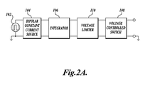
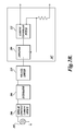
- FIGURES 2A and 2B are block diagrams of transmitters that may be used in the practice of the invention.
- a pulse generator 102 supplies a sequence of signal pulses to a current source 104.
- each sequence of pulses supplied by pulse generator 102 consists of two or more pulses having a predefined timing relationship and duration.
- the pulse generator may comprise a digital circuit or programmed processor that operates as a controller to output a sequence of three signal pulses.
- the pulse generator preferably spaces the timing of the signal pulses so as to avoid overheating the transmitter and so that the signal pulses to not occur at times that are harmonically related to the signals on the branch circuit or at times where noise in the branch circuit is likely to occur (e.g. at voltage peaks or minimums).
- the signal pulses can be output at time intervals that are predefined but are not equal to each other such that the time between successive pairs of signal pulses is not the same.
- the transmitter can include a zero crossing detector for detecting zero signal crossings on the branch circuit.
- the transmitter then outputs the signal pulses at times that are defined with respect to a detected zero crossing.
- the transmitter preferably outputs the signal pulses when the phase of the branch circuit into which the current pulses are to be induced is positive and the other phases of the 3-phase system are negative.
- the zero crossing detector does not detect a zero crossing within a certain amount of time and the transmitter is then programmed to output the sequence of signal pulses at predetermined times with respect to the first pulse.
- current source 104 is a bipolar constant current source (also referred to as a "current pump”), which can produce current flow in either direction (i.e., can function both as a current source and a current sink).
- current source 104 For each pulse provided by pulse generator 102, current source 104 generates a rectangular current pulse, which is supplied to an integrator circuit 106.
- integrator 106 periodically receives a sequence of two or more constant current pulses.
- integrator 106 supplies a linearly increasing voltage to a voltage controlled switch 108 via a voltage limiter 110.
- the output terminals of voltage controlled switch 108 connect to a branch circuit that is to be traced to its associated circuit interrupter by means of a connector such as conductors 82 of transmitter 80 in FIGURE 1 .
- the linearly increasing voltage signal supplied by integrator 106 linearly drives voltage controlled switch 108 toward a conductive state.
- voltage limiter 110 establishes the maximum voltage that can be supplied to voltage controlled switch 108 by integrator 106.
- limiter 110 limits the current flow that is induced in a branch circuit to a predetermined maximum value.
- the voltage supplied by integrator 106 linearly decreases.
- the time interval between the current pulses generated by current source 104 is such that the output voltage supplied by integrator 106 causes voltage controlled switch 108 to be turned off.
- the duration of the current pulses generated by constant current source 104 is such that voltage controlled switch 108 is in a conductive state for a relatively short period of time. That is, current pulses of relatively short duration are induced in a branch circuit that is being traced. For example, current pulses having rise and fall times on the order 65 microseconds and a pulse duration on the order of 200 microseconds may be used.
- the transmitter shown in FIGURE 2B includes a pulse generator 102, a current source 104, an integrator 106, and a voltage limiter 110 that are connected in the same manner as is shown in FIGURE 2A and that operate as described above.
- the difference between the two depicted arrangements being that the arrangement of FIGURE 2B utilizes a current controlled switching circuit 107 in place of the voltage controlled switch 108 that is employed in the arrangement of FIGURE 2A .
- the output of voltage limiter 110 in FIGURE 2B is connected to the non-inverting input terminal of an amplifier 109 that supplies a signal to the input terminal of a current controlled switch 111.
- one output terminal of current controlled switch 111 is connected to the hot lead of a branch circuit that is to be traced.
- the other output terminal of the current controlled switch is connected to the inverting input terminal of amplifier 109 and, in addition, to the neutral lead of the branch circuit via a resistor 113.
- the current supplied to current controlled switch 111 is directly proportional to the voltage supplied by voltage limiter 110.
- current controlled switch 111 operates to linearly switch between conductive and nonconductive states in the same manner as voltage controlled switch 108 of FIGURE 2A .
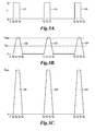
- FIGURES 3A-3C depict operation of the arrangement of FIGURE 2 wherein pulse generator 102 periodically supplies three signal pulses that result in the generation of three corresponding constant current pulses by bipolar constant current source 104 (signal pulses 112, 114, and 116 in FIGURE 3A ).
- integrator 106 supplies three voltage pulses (120, 122 and 124 in FIGURE 3B ) to the input of voltage control switch 108 of FIGURE 2A .
- the voltage pulses switch voltage controlled switch 108 of FIGURE 2A (or, alternatively, current controlled switch 111 of FIGURE 2B ) between conductive and nonconductive (ON and OFF) states in a substantially linear fashion.
- voltage controlled switch 108 or current controlled switch 111
- current pulse 112 switches from an initial negative current (-Ip) to supply a constant positive current (+Ip) during time interval (t 01 -t 03 ).
- the output voltage 120 provided by integrator 106 rises linearly from an initial negative value (-V).
- the output voltage of integrator 106 is clamped to a value V MAX by the limiter circuit 120 of FIGURES 2A or 2B to establish the maximum voltage applied to the input of voltage controlled switch 108 (or maximum current drive to current controlled switch 111).
- the operation of a transmitter that employs a current controlled switch 111 differs from what is described above for voltage controlled switch 108 in that (a) the amplifier 109 of FIGURE 2B provides an output current that is directly proportional to the signal produced by voltage limiter 110 (i.e., voltage pulse 120 of FIGURE 3B ); and (b) the current provided by amplifier 109 linearly drives the current controlled switch to produce current pulse 126 of FIGURE 3C .
- the operation described relative to time interval t 01 to t 04 is repeated during time intervals t 11 -t 14 (constant current pulse 114 in FIGURE 3A ) and during the time interval t 20 - t 24 (constant current pulse 116 in FIGURE 3A ).
- the pulse sequence described relative to FIGURE 3 induces three current pulses 126, 128 and 130 in a branch circuit that is being traced.
- the idealized constant current pulses are identical in pulse duration and amplitude. However, the depicted current pulses do not exhibit a constant pulse repetition rate.
- the time interval between the first and second pulse and the time interval between the second and third pulse are not equal to one another.
- either equally spaced or unequally spaced current pulses may be employed.
- unequal spacing of the current pulses can provide improved immunity from signal pulses that are induced in branch circuits of an electrical distribution system by devices such as light dimmers, motors and other such devices.
- FIGURE 4A depicts a schematic diagram of one realization of the transmitter arrangement of FIGURE 2A , thus depicting an arrangement that can be employed as transmitter 80 of FIGURE 1 .
- the constant current source 104 of FIGURE 2A is a voltage controlled constant current source 132 that is within a class of circuits known as Howland current pumps.
- the depicted Howland current pump includes an operational amplifier 134. Connected between the output terminal of operational amplifier 134 and the non-inverting input is a positive feedback path consisting of serially connected resistors 136 and 138. Negative feedback is provided by resistor 140, which is connected between the output and inverting input terminals of operational amplifier 134.
- the inverting input terminal of operational amplifier 134 is connected to an input terminal 143 via a resistor 142 and the non-inverting input of operational amplifier 134 is connected to an input terminal 145 via a resistor 144.
- the input resistors of a Howland current pump are typically equal in resistance value and are substantially greater in resistance than the resistance in the positive and negative feedback paths (resistance of resistor 140 in the negative feedback path and the sum of the resistance values of resistors 136 and 138 in the positive feedback path).
- the resistance value of feedback resistor 140 is usually equal to the sum of the resistance values of positive feedback resistors 136 and 138.
- the resistance value of the two input resistors (142 and 144 in FIGURE 4A ) should closely match one another and the resistance value of negative feedback path resistor (140 in FIGURE 4A ) should closely match the sum of the resistance values in the positive feedback path (resistors 136 and 138).
- the current supplied by a Howland current pump is proportional to the difference between the voltages that are supplied to the circuit input terminals (terminals 143 and 145, in FIGURE 4A ).
- a positive DC potential is supplied to input terminal 143 (indicated by battery 146 but may be provided by a circuit that produces an accurate voltage signal) and a pulse generator 148 that supplies positive going voltage pulses is connected to input terminal 145.
- the DC potential supplied to terminal 143 is equal to the one half of the peak voltage of the pulses supplied by pulse generator 148.
- the rise and fall times of the integrated current pulses will be substantially equal (e.g., the rise and fall times of voltage pulses 120, 122 and 124 in FIGURE 3B ).
- the voltage controlled switch (108 in FIGURE 2 ) is an N-channel enhancement mode metal oxide field effect transistor (MOSFET) 150 that is switched between non-conducting and conducting states by current pulses that are provided by voltage controlled constant current source 132.
- MOSFET 150 N-channel enhancement mode metal oxide field effect transistor
- the gate electrode of MOSFET 150 is connected to the junction between resistors 136 and 138 of voltage controlled constant current source 132.
- pulse generator 148 of FIGURE 4A causes voltage controlled constant current source 132 to supply a positive current (e.g., current +I p in FIGURE 3A )
- V the voltage supplied to the gate electrode of MOSFET 150
- C the gate to source capacitance of MOSFET 150
- i the capacitor charging or discharging current.
- the current I p that is supplied to the gate of MOSFET 150 remains constant during time intervals t 01 -t 03 t 11 -t 13 and t 21 -t 23. .
- the gate voltage of MOSFET 150 linearly increases at a time rate of change equal to I p / C during each of these intervals to produce the linear increases in the current pulses 126, 128 and 130 that are shown in FIGURE 3C .
- MOSFET 150 is linearly discharged during time intervals t 03 -t 04 , t 13 -t 14 and t 23 -t 24 .to cause a linear decrease in the current pulses 126, 128 and 130 at a time rate of change that also is equal to I p / C .
- the voltage limiting function described relative to voltage limiter 110 of FIGURE 2A is implemented by an NPN transistor 154.
- the collector electrode of NPN transistor 154 is connected to the junction between resistors 136 and 138 of voltage controlled constant current source 132; the emitter of NPN transistor 154 is connected to circuit common (ground); and the base electrode of the transistor is connected to the source electrode of MOSFET 150.
- the source electrode of MOSFET 150 is connected to circuit common (ground) via a resistor 156.
- NPN transistor 154 operates in the following manner to limit the voltage at the gate electrode of MOSFET 150 and, hence, establish the maximum current of the current pulses induced in a branch circuit that is being traced (e.g., current I MAX of current pulses 126, 128 and 130 in FIGURE 3C ).
- current I MAX of current pulses 126, 128 and 130 in FIGURE 3C current I MAX of current pulses 126, 128 and 130 in FIGURE 3C .
- voltage controlled constant current source 132 supplies positive current flow
- the gate to source capacitor of MOSFET 150 charges.
- the branch circuit causes a rapid increase in the drain to source current of MOSFET 150.
- the drain to source current causes NPN transistor 154 to conduct and thereby limit the gate voltage of MOSFET 150.
- the resistance of resistor 156 in the arrangement of FIGURE 4A is relatively low and is selected to turn on NPN transistor 154 at a desired level of drain-to-source current flow through MOSFET 150.
- the resistance value of resistor 156 was 0.105 ohms.
- FIGURE 4B schematically depicts an embodiment of a transmitter that corresponds to the arrangement shown in FIGURE 2B , thus depicting an alternative to the above described arrangement of FIGURE 4A .
- a pulse generator 148 is connected to a voltage controlled constant current source 132 (e.g., a Howland current pump) in the same manner as described relative to FIGURE 4A .
- the output of voltage controlled constant current 132 is a sequence of constant current pulses such as current pulses 112, 114 and 116 of FIGURE 3A .
- a capacitor 161 is connected between the output terminal of voltage controlled constant current source 132 and circuit common.
- a voltage limiter 163 is connected to capacitor 161 to clamp the maximum positive and negative capacitor voltages at predetermined values.
- voltage limiter 163 is a conventional clipper circuit that includes a diode 165 with the anode connected to capacitor 161 and the cathode connected to a positive voltage (+V LIMIT in FIGURE 4B ).
- the cathode of a second diode 167 is connected to capacitor 161 with the anode being connected to a negative voltage (-V LIMIT in FIGURE 4B ).
- the current supplied by voltage controlled constant current source 132 flows through diode 165 to clamp the capacitor voltage at a predetermined level (e.g., V MAX at time t 02 in FIGURE 3B ).
- the capacitor voltage remains clamped throughout the remaining period of time that voltage controlled current source 132 supplies a positive output current (e.g., time interval t 02 -t 03 in FIGURE 3A ).
- voltage controlled current source 132 switches between a positive and negative output current (e.g., at time t 03 in FIGURE 3A )
- the current source acts as a current sink and capacitor 161 begins to charge in the negative direction with the capacitor voltage decreasing at a rate equal to I p / C , where C is the capacitance of capacitor 161.
- the time rate of change of increasing capacitor voltage is identical to the time rate of change of decreasing capacitor voltage.
- the output current of constant current source 132 flows through diode 167 to clamp the voltage of capacitor 161 at one diode drop below -V LIMIT (e.g., at a value that corresponds to -V in FIGURE 3B ).
- Current continues to flow through diode 165, maintaining the capacitor voltage at it maximum negative voltage (e.g., -V) until voltage controlled current source 132 again supplies a positive output current (e.g., at time t 11 in FIGURE 3A ).
- the current controlled switching circuit 107 of FIGURE 2B is implemented by an operational amplifier 169 and an NPN transistor 171.
- the non-inverting input terminal of amplifier 169 is supplied with the above described signal provided by capacitor 161 and the amplifier output is coupled to the base electrode of NPN transistor 171.
- the emitter electrode of transistor 171 is coupled to the inverting input terminal of amplifier 169 and, in addition, is connected to a first output terminal of the depicted current controlled switching circuit via a resistor 173.
- the second output terminal of the depicted switching circuit is directly connected to the collector electrode of NPN transistor 171.
- Operational amplifier 169 functions as a unity gain voltage follower that drives transistor 171.
- V C is the voltage supplied by capacitor 161
- R 173 is the resistance value of resistor 173.
- capacitor 161 supplies sequences of voltage pulses of the type shown in FIGURE 3B , it can be seen that the arrangement of FIGURE 4B induces current pulses in the branch circuit being traced that correspond to current pulses 126, 128 and 130 of FIGURE 3C in that the current pulses exhibit equal rise and fall times and linearly increase and decrease at a rate determined by the integration of constant current pulses.
- receivers that are configured for use with those transmitters.
- the basic configuration and operation of a receiver that is suitable for use in the invention can be understood in view of the type of current pulse sequences that are used in the practice of the invention.
- receivers used in the practice of the invention are battery powered handheld devices that include a pickup coil for sensing the current pulses induced in a branch circuit by the system transmitter.
- the receiver is placed proximate candidate circuit interrupters until a signal is electromagnetically coupled to the pickup coil that corresponds to the current pulses supplied by the system transmitter.
- Receivers that are configured and arranged to operate in accordance with this invention process each sequence of current pulses induced in a branch circuit in accordance with the invention: (1) to detect the occurrence of the first pulse of a received sequence of current pulses; and, (2) to sample the signal received (induced in the receiver pickup coil) during periods of time at which the subsequent pulses of a sequence of current pulses would be expected to occur.
- the receive signal is sampled during a first sampling interval that begins at a time that is less than or equal to time t 11 and ends at a time that is equal to or greater than time t 14 in order to detect current pulse 128 of FIGURE 3C .
- the received signal is sampled for a second time during an interval that is less than or equal to t 21 and equal to or greater than t 24 in order to detect current pulse 130 of FIGURE 3C .
- Generating and sampling a sequence of current pulses in the described manner provides enhanced rejection of electrical system current pulses that are not induced by the system transmitter, thereby reducing the probability of falsely indicating that a circuit interrupter is the circuit interrupter associated with a branch circuit that is being traced. Specifically, a receiver operating in the described manner will not produce a signal indicating that a circuit interrupter has been located unless a sequence of current pulses is detected that at least closely matches the separation in time between the current pulses induced by the system transmitter.
- the receivers of the currently preferred embodiments of the invention function to determine whether the pulse width of each pulse in a received sequence of current pulses substantially corresponds to the pulse width of the current pulses induced by the system transmitter. Even further improvement is attained by sensing the amplitude of each pulse in a received sequence of current pulses to determine whether the received pulse amplitudes fall within an expected range that is based on the amplitudes of the current pulses induced in a branch circuit by the system transmitter.
- the resistive component of the impedance of the pickup coil is substantially less than the inductive component.
- the pickup coil differentiates the received current pulses to produce positive going and negative going signal pulses of generally rectangular shape for each current pulse in a sequence of current pulses.
- FIGURE 5 is a circuit diagram depicting an exemplary receiver circuit configured to perform the above-discussed processing of sequences of current pulses that are induced in a branch circuit in accordance with the invention.
- a pickup coil 160 is connected to the inverting input of an operational amplifier 162 via a resistor 164.
- a resistor 166 is connected between the inverting input terminal and the output terminal of operational amplifier 162 to provide negative feedback and a resistor 168 is connected between the inverting input terminal of operational amplifier 162 and circuit common.
- the inductance of pickup coil 160 is relatively low so that the transfer function of the circuit stage that includes pickup coil 160 and operational amplifier 162 corresponds to a first order filter in which the output provided by operational amplifier 162 increases with respect to increasing frequency of the signal that is electromagnetically coupled to pickup coil 160 from a branch circuit that is being traced.
- the frequency of the AC signal being supplied is below the filter function cutoff frequency.
- the inductance of pickup coil 160 was 556 microHenries.
- FIGURE 6A and FIGURE 6B respectively depict a series of current pulses induced in a branch circuit in accordance with the invention and the signal supplied by operational amplifier 162 of FIGURE 5 .
- FIGURE 6A depicts a sequence of three current pulses 170, 172, and 174 of the type induced in a branch circuit being traced.
- each current pulse includes a linearly increasing leading edge (e.g., time t 01 -t 02 in current pulse 170), a constant current interval (t 02 -t 03 ) and a linearly decreasing trailing edge (t 03 -t 04 in current pulse 170).
- the voltage developed across an inductor is proportional to the first derivative with respect to time of the current that flows through the inductor.
- the pickup coil differentiates the current pulses that are induced in a branch current that is being traced.
- a generally rectangular negative pulse is supplied by pickup coil 160 of FIGURE 5 (and hence operational amplifier 162) during the linearly increasing portion of each current pulse 170, 172, and 174 of FIGURE 6A ; no output (zero volts) is supplied by the pickup coil and operational amplifier 162 during the interval of time in which the current pulses exhibit a constant current; and, a generally rectangular positive voltage pulse is supplied by pickup coil 160 during the linearly decreasing portions of each current pulse 170, 172, and 174 in FIGURE 6A .
- the voltage pulses supplied at the output terminal of operational amplifier 162 are coupled to an amplifier stage that includes an operational amplifier 184.
- the sequence of negative and positive rectangular voltage pulses supplied at the output terminal of operational amplifier 162 is coupled to the non-inverting input terminal of operational amplifier 184 via a resistor 186.
- a resistor 188 Connected between the output and inverting input terminals of operational amplifier 184 is a resistor 188.
- a resistor 190 Connected between the inverting input terminal of operational amplifier 184 and circuit common is a resistor 190.
- Connected in parallel with resistor 190 is a resistor 192 and the drain to source current path of an N-channel enhancement mode MOSFET 194.
- the voltage gain of operational amplifier 184 is controlled by the drain to source resistance of MOSFET 194.
- the gain of the circuit stage can be adjusted by controlling the gate voltage supplied to MOSFET 194 with a potentiometer or other arrangement for providing a range of voltages (not shown in FIGURE 5 ).
- the voltage pulses provided at the output terminal of operational amplifier 184 are coupled to the non-inverting input of an operational amplifier 196 via a resistor 198.
- a feedback path is formed between the output and inverting input terminals of operational amplifier 196 by a resistor 200.
- Operational amplifier 196 functions as a half wave rectifier to eliminate the negative pulses of the signal provided by operational amplifier 184.
- the output of operational amplifier 196 that corresponds to current pulses 170, 172, and 174 of FIGURE 6A is a sequence of three positive rectangular voltage pulses 204, 206, and 208.
- the timing of the rectangular voltage pulses provided by operational amplifier 196 corresponds to the timing of the detected current pulses 170, 172, and 174 of FIGURE 6A .
- the time interval t 04 -t 14 denotes the time interval between the end of the first current pulse 170 and the second current pulse 172 and also denotes the time interval between the end of the first voltage pulse 204 and the second voltage pulse 206.
- time interval t 14 -t 24 denotes the time interval between the end of the second current pulse 172 and the third current pulse 174 of FIGURE 6A and additionally denotes the time interval between the end of the second rectangular voltage pulse 206 and the third rectangular voltage pulse 208 of FIGURE 6C .
- voltage pulses 204, 206 and 208 are representative of current pulses 170, 172 and 174 in that the temporal relationship between the voltage pulses corresponds to the temporal relationship between the current pulses.
- positive voltage pulses 204, 206 and 208 are supplied by operational amplifier 196 to an input terminal of a micro controller 202 and, in addition, to the input terminals of a pair of sample and hold circuits.
- receivers that are configured and arranged in accordance with this invention function to process each sequence of current pulses that a transmitter induces in a branch circuit to determine whether the timing of the received current pulses substantially corresponds to the timing of the current pulses induced in a branch circuit by the system transmitter.
- the receiver produces an indication that the proper circuit interrupter has been located only if the timing of the received sequence of current pulses closely matches the timing of the current pulses induced in a branch circuit by the system transmitter.
- the receiver preferably determines whether the pulse width of each current pulse is substantially the same as the pulse width of the current pulses provided by the system transmitter. Further, the receiver preferably senses the amplitude of received current pulses and produces an indication that the proper current interrupter has been located only if the amplitudes of the received current pulses fall within an expected range of amplitudes.
- microcontroller 202 functions in conjunction with switch circuits 210 and 212 to establish signal sampling intervals that are used to determine whether the timing between pulses in a received sequence of the current pulses sufficiently corresponds to the timing of a sequence of transmitted current pulses (i.e., a sequence of current pulses induced in the branch circuit being traced).
- FIGURE 6D diagrammatically depicts operation of the circuit arrangement of FIGURE 5 for the sequence of signal pulses described above relative to FIGURES 6A-C .
- a RESET pulse is generated by microcontroller 202 at time t 04 , which corresponds to the trailing edge of rectangular voltage pulse 204 of FIGURE 6C .
- the RESET pulse is coupled to switch 210 and 212, which results in switches 210 and 212 to switch to an open-circuit condition.
- the RESET pulse serves as a trigger to cause microcontroller 202 to generate two gate signals (GATE 1 and GATE 2) in FIGURES 5 and 6D .
- the GATE 1 signal causes switch 210 to switch to the closed-circuit state for the duration of the GATE 1 signal and the GATE 2 signal places switch circuit 212 in the closed-circuit condition for the duration of the GATE 2 signal.
- the first gate signal, GATE 1 begins at a time that is slightly less than time t 13 and ends at a time that is somewhat greater than time t 14 .
- the second gate signal, GATE 2 begins at a time that is slightly less than time t 23 and ends at a time that is somewhat greater than time t 24 .
- switch 210 will supply a signal identical to the signal provided by operational amplifier 196 while the GATE 1 signal is present and switch 212 (time interval t 13 -t 14 of FIGURE 6 ) and will supply the signal provided by operational amplifier 196 during the duration of the GATE 2 signal (t 23 -t 24 ).
- switches 210 and 212 respectively function to provide signal samples that are representative of the signal provided by pickup coil 160 of receiver 90 during time intervals t 13 - t 14 and t 23 -t 24 .
- the output of switch 210 is connected to the non-inverting input terminal of an operational amplifier 214, which has its output terminal connected to the amplifier inverting input terminal via a diode 211.
- diode 211 feeds the positive going portions of the operational amplifier output signal back to the amplifier inverting input terminal so that operational amplifier 214 provides an output signal that is substantially identical to the positive going portion of the signal provided to operational amplifier 214.
- the cathode of diode 211 is connected to circuit common via a resistor 215 and a signal path that is connected in parallel with resistor 215 and that includes a series-connected combination of a capacitor 217 and a resistor 219.
- capacitor 217 charges to the peak value of the signal that is supplied by operational amplifier 196 during the time interval t 13 -t 14 of FIGURE 6 and holds that value until microcontroller 202 generates another RESET pulse (not shown in FIGURE 6 ).
- switch 210 and the circuit that includes operational amplifier 214 operate in conjunction with one another to serve as a sample and hold circuit that holds a dc voltage representative of the signal produced by receiver pickup coil 160 during the time interval t 13 - t 14 .
- the circuit topology that is connected to switch 212 corresponds to the above describe circuit arrangement that is connected to the output of switch 210.
- the output of switch 212 is connected to the non-inverting input terminal of an operational amplifier 216, which has its output terminal connected to the amplifier inverting input terminal via a diode 221.
- diode 221 feeds the positive going portions of the operational amplifier output signal back to the amplifier inverting input terminal so that operational amplifier 214 provides an output signal that substantially identical to the positive going portion of the signal provided to operational amplifier 214.
- the cathode of diode 221 is connected to circuit common via a resistor 223 and a signal path that is connected in parallel with resistor 223 and that includes a series-connected combination of a capacitor 225 and a resistor 229.
- capacitor 225 charges to the peak value of the signal that is supplied by operational amplifier 196 during the time interval t 23 -t 24 of FIGURE 6 and holds that value until microcontroller 202 generates another RESET pulse (not shown in FIGURE 6 ).
- switch 212 and the circuit that includes operational amplifier 216 operate in conjunction with one another to serve as a sample and hold circuit that holds a dc voltage representative of the signal produced by receiver pickup coil 160 during the time interval t 23 - t 24 .
- the signal sample provided at the juncture between capacitor 217 and diode 211 is coupled to the input terminal of a comparator 218 via a resistor 220.
- the signal sample provided at the junction between capacitor 225 and diode 221 is coupled to the input terminal of comparator 218 via a resistor 222.
- the input signal supplied to comparator 218 is equal to sum of the signal samples provided by the above described receiver circuitry during the time intervals t 13 - t 14 and t 23 - t 24 in the timing diagram ofFIGURE6.
- Comparator 218 of FIGURE 5 includes an operational amplifier 224 having a resistor 226 connected between the amplifier output terminal and the inverting input terminal.
- a variable resistor 228 is connected between the amplifier non-inverting input terminal and circuit common.
- Connected to the output terminal of operational amplifier 242 is the gate electrode of an N-channel enhancement mode MOSFET 230.
- variable resistor 228 can be set so that the output voltage of operational amplifier 224 does not turn on MOSFET 230 unless the sum of the signals supplied by sample and hold circuits 210 and 212 exceeds a predetermined level.
- variable resistor 228 can be set so that operational amplifier 224 of comparator provides a positive gate signal to MOSFET 230 when a sequence of current pulses detected by the system receiver (e.g., the above discussed arrangement of FIGURE 5 ) sufficiently correspond to a sequence of current pulses induced in the branch circuit being traced.
- the required correspondence is with respect to the timing between pulses, pulse duration, and pulse amplitude.
- the GATE 1 signal supplied by microcontroller 202 ( FIGURE 6D ) is established so that it begins slightly before time t 13 and ends shortly after time t 14 .
- the voltage pulse 206 of FIGURE 6C that is produced by operational amplifier 196 of FIGURE 5 in response to current pulse 172 occurs during (and is substantially equal in duration to) the GATE 1 signal.
- the GATE 2 signal supplied by microcontroller 202 is established so that it begins slightly before time t 23 and ends shortly after time t 24 .
- the voltage pulse 208 of FIGURE 6C that is produced by operational amplifier 196 of FIGURE 5 in response to current pulse 174 occurs during (and is substantially equal in duration to) the GATE 2 signal.
- the signal supplied to the input terminal of comparator 218 slightly after time t 14 (at the conclusion of the GATE 1 signal) is a dc voltage representative of the signal produced by pickup coil 160 during the period of time in which the second current pulse (172 in FIGURE 6A ) is induced in the branch circuit being traced.
- the signal supplied to the input terminal of comparator 218 increases at the conclusion of the GATE 2 signal (slightly after time t 24 ) by an amount that is representative of the signal produced by pickup coil 160 during the period of time in which the third current pulse (174 in FIGURE 6A ) is induced in the branch circuit being traced.
- the invention can be embodied so that comparator 218 turns on MOSFET 230 when the timing of the signal pulses produced by the circuitry of receiver 90 sufficiently corresponds to the timing of the current pulses induced in a branch circuit being traced (e.g., current pulses 170, 172 and 174 in FIGURE 6A ).
- both the pulse width relationship and the pulse timing relationship that exists between the current pulses induced in a branch circuit being traced and the current pulses detected by the receiver are used to determine the voltage input to comparator 218 that will switch MOSFET 230 to the ON state.
- the amplitude of the pulses produced by the circuitry of receiver 90 are directly related to the amplitude of the current pulses induced in the branch circuit being traced.
- comparator 218 switches MOSFET 230 to the ON state only if the signal supplied to the comparator input indicates reception of a series of current pulses that correspond to a series of current pulses induced in a branch circuit being traced with respect to pulse timing, pulse width and pulse amplitude.
- the source electrode of MOSFET 230 is connected to an output port of microcontroller 202 (labeled ERR in FIGURE 5 ) and the drain electrode is connected to a positive supply voltage labeled BATT+ via a resistor 232.
- microcontroller 202 is programmed to maintain the ERR output port at circuit common (ground potential) during normal operation of the depicted receiver circuit.
- comparator 218 switches MOSFET 230 to the ON state, the voltage at the junction of resistor 232 and the MOSFET drain electrode decreases from a value approximately equal to BATT+ to a value at or near circuit common.
- MOSFET 234 Also connected to the BATT+ supply voltage is the source electrode of a P-channel enhancement mode MOSFET 234 having its gate electrode connected to the junction between resistor 232 and the drain electrode of MOSFET 230.
- MOSFET 230 When MOSFET 230 is switched to the ON state (to designate the detection of the circuit interrupter of the branch circuit being traced), the gate to source voltage of MOSFET 234 becomes negative to drive MOSFET 234 into conduction.
- a positive voltage is supplied to the anode of a light emitting diode, which is connected to the drain electrode of MOSFET 234.
- the arrangement of FIGURE 5 also includes an exemplary audible indicator circuit 240 for indicating detection of the circuit interrupter associated with a branch circuit being traced.
- Audible indicator 240 of FIGURE 5 includes a multivibrator formed by an inverting Schmitt trigger circuit 242 having a resistor 244 connected between its output and input terminals. A capacitor 246 is connected between the input terminal of Schmitt trigger circuit 242 and circuit common.
- the multivibrator arragement included in audible indicator produces a square wave signal at a frequency that is dermined by the RC time constant of resistor 244 and capacitor 26, whenever an operating voltage (BATTSW in FIGURE 5 ) is supplied to Schmitt trigger circuit 242. Since BATTSW is supplied only when MOSFET 234 is in the conducting state, it can be recognized that Schmitt trigger circuit 242 will provide a square wave signal when a circuit interrupter is located that is associated with the branch circuit being traced.
- the square wave signal supplied by Schmitt trigger circuit 242 is coupled to the input terminal of an inverter ciruit 248. Connected between the output and input terminals of inverter 248 is a transducer 250 for producing an an audible audio output signal.
- a transducer referred to as an external drive piezoelectric diaphram was employed as transducer 250.
- Schmitt trigger ciruit 242 produces a square wave signal when the circuit interrupter that is associated with the branch circuit being traced has been located.
- the exemplary receiver arrangement of FIGURE 5 provides an audible signal indication as well as the visual indication provided by light emitting diode 236 when the circuit interrupter being sought has been located.
- FIGURE 7 is a flow diagram that provides a summary of the exemplary arrangement of the invention that is shown and described relative to FIGURES 1-6 .
- exact correspondence to the steps described relative to FIGURE 7 is not a required aspect of the invention, but simply provides one example of how the invention can be implemented.
- the receiver circuit of FIGURE 5 is advantageous in that the combined use of digital and analog circuitry provides a high degree of immunity with respect to signals induced in the branch circuits of a power distribution system by motors, light dimmers and other devices.
- the invention may be implemented entirely with analog or digital techniques.
- circuitry used to implement the invention and the exemplary processing described relative to FIGURE 7 process a sequence of current pulses that generally correspond to the pulse shape that is shown in idealized form and described relative to FIGURE 3C , and do so, in the manner described relative to FIGURES 6B-D .
- the process begins at START block 260, with the pickup coil of the receiver circuitry being held in close proximity to a circuit interrupter that may be associated with a branch circuit that is being traced.
- the receiver circuitry determines whether a current pulse is present. If no pulse is present, the receiver circuitry, in effect, waits for a pulse to arrive.
- the process is shown as returning to START block 260 via block 264, which may be used to perform a function such as setting the ERR signal provided by microcontroller 202 of FIGURE 5 to a value that prevents energizing the receiver indicator circuits (e.g., audible indictor 240 and light emitting diode 236 of FIGURE 5 ).
- the duration of the pulse is determined at block 266. If the detected pulse width sufficiently matches the width of a current pulse induced in a branch circuit by the system transmitter (e.g., is within system design tolerance), a gate signal, (such as GATE 1 of FIGURE 6D ) is generated. In FIGURE 7 , the gate signal is set at block 268 and is established so that the receiver circuitry will determine whether a pulse is being received at a time that corresponds to the time at which the next current pulse is expected.
- the sequence returns to start block 260.
- the sequence also returns to the start block if it is determined at block 272 that the pulse width of the pulse received by the receiver pickup coil does not sufficiently match the duration of a current pulse supplied by the system transmitter. In either case the sequence of FIGURE 7 begins again when the next pulse arrives at the receiver pickup coil, If the pulse duration determined at block 272 sufficiently matches a transmitted current pulse, a signal representative of the amplitude of the pulse is stored (at block 274). This point in the sequence of FIGURE 7 corresponds to the sample and hold operation described in terms of FIGURES 5 and 6 relative to switch 210 and the circuitry that includes operational amplifier 214.
- a second gate signal is set (at block 276) so that the signal that is coupled to the receiver pickup coil will be sensed during a time duration that corresponds to the time period during which the next current pulse supplied by the system transmitter should arrive. If a pulse is not detected during the second gate period (at block 278), the sequence returns to start block 260 and begins again upon the detection of another current pulse. On the other hand, if a pulse is detected during the second gate period, a determination is made as to whether the pulse duration sufficiently matches the duration of a current pulse supplied by the system transmitter (at block 280). If the pulse duration is not of the proper duration, the sequence reverts to start block 260 to begin again when the next current pulse is detected.
- a signal representative of the amplitude of the pulse is stored (at block 282).
- This point in the sequence of FIGURE 7 corresponds to the sample and hold operation described in terms of FIGURES 5 and 6 relative to switch 212 and the circuitry that includes operational amplifier 216. Specifically, a sequence of three consecutive current pulses have been detected that likely correspond to a sequence of three current pulses that have been induced in a branch circuit being traced.
- the signals that are representative of the amplitudes of the two detected current pulses are summed with one another, with the result being compared with a predetermined range of values that indicates that two received current pulses sufficiently correspond to two current pulses that were supplied by the system transmitter. If the comparison indicates that the sum of the two signals is outside an acceptable range, the sequence returns to start block 260 to begin again when a current pulse is coupled to the receiver pickup coil. If the comparison indicates that the two received current pulses sufficiently correspond to two current pulses that were supplied by the system transmitter, the receiver pickup coil is positioned proximate the circuit interrupter that is associated with the branch circuit being traced and a suitable audible and/or visual indication is generated (indicated at block 286).
- the invention provides reliable detection of the circuit interrupter of a branch circuit being traced.
- the circuit interrupters of conventionally configured power distribution panels are arranged in rows with a bus bar that provides power to the panel extending vertically to divide the distribution panel into left and right portions.
- current flows from left to right through the circuit interrupters on the right side of the bus bar and current flows from right to left through the circuit interrupters that are located on the left side of the bus bar.
- the direction of incident magnetic flux (and resulting current flow) that is induced in a pickup coil reverses when the pickup coil is moved between the right and left sides of the distribution panel.
- the flux reversal means that the pickup coil must be rotated by 180 degrees when it is moved between the two sides of a distribution panel so that that induced flux is in a required direction.
- transmitters configured in accordance with the an embodiment of the invention produce a sequence of current pulses in which each current pulse linearly increases to a maximum value, remains at the maximum current value for a predetermined time, and then linearly decreases with a fall time that is equal to the pulse rise time. Examples of the current pulses are depicted in and were described relative to FIGURE 3C .
- receivers configured in accordance with an embodiment of the invention differentiate the current pulses to produce equal duration positive-going and negative-going rectangular voltage pulses that are separated from one another by an interval of time that is equal to the period of time that the current pulses that are supplied by the transmitter remain at maximum current. Examples of such voltage pulses are shown in idealized form in FIGURE 6B .
- Half-wave rectification provided by the operational amplifier 196 eliminates the negative-going voltage pulses, thus converting a sequence of current pulses supplied by the system transmitter into a corresponding sequence of positive-going substantially rectangular voltage pulses.
- the receiver produces positive-going pulses on either the rising edge or the falling edge of the current pulse waveforms depending on the direction of current flow though the circuit interrupter.
- the receiver operates correctly regardless of which direction the current flows. Accordingly, in the practice of the invention, there is no need to rotate the receiver pickup coil by 180 degrees when moving it from one side of the distribution panel to the other. Although the preferred embodiment uses equal rise and fall times, it will be appreciated that the transmitter and receiver could operate where only the rise or the fall time of each current pulse is predefined for each current pulse.
- the time rate of change in the induced current pulse is established by the integration of constant current pulses, such as those provided by voltage controlled constant current source 132.
- constant current pulses such as those provided by voltage controlled constant current source 132.
- the gate to source capacitance of MOSFET 150 is selected in view of the maximum positive and negative currents provided by voltage controlled current source 132 to thereby establish a desired time rate of current change in the pulses that are induced in branch circuit being traced.
- the capacitance of capacitor 161 is selected in view of the maximum positive and negative currents provided by voltage controlled current source 132 to thereby establish a desired time rate of current change in the induced current pulses.
- the rise and fall times of the induced current pulses preferably are established in view of the time constant associated with the receiver pickup coil (e.g., pickup coil 160 of FIGURE 5 so that the voltage produced by the pickup coil is representative of the maximum value of the induced current pulses.
Landscapes
- Physics & Mathematics (AREA)
- General Physics & Mathematics (AREA)
- Measurement Of Current Or Voltage (AREA)
- Remote Monitoring And Control Of Power-Distribution Networks (AREA)
- Locating Faults (AREA)
Applications Claiming Priority (1)
| Application Number | Priority Date | Filing Date | Title |
|---|---|---|---|
| US12/537,873 US8339272B2 (en) | 2009-08-07 | 2009-08-07 | Circuit breaker locator |
Publications (2)
| Publication Number | Publication Date |
|---|---|
| EP2290384A2 true EP2290384A2 (fr) | 2011-03-02 |
| EP2290384A3 EP2290384A3 (fr) | 2013-01-23 |
Family
ID=43301940
Family Applications (1)
| Application Number | Title | Priority Date | Filing Date |
|---|---|---|---|
| EP10170698A Withdrawn EP2290384A3 (fr) | 2009-08-07 | 2010-07-23 | Localisateur de disjoncteurs |
Country Status (4)
| Country | Link |
|---|---|
| US (1) | US8339272B2 (fr) |
| EP (1) | EP2290384A3 (fr) |
| CN (1) | CN101995548A (fr) |
| TW (1) | TW201120465A (fr) |
Cited By (3)
| Publication number | Priority date | Publication date | Assignee | Title |
|---|---|---|---|---|
| EP2554948A3 (fr) * | 2011-08-03 | 2014-12-10 | General Electric Company | Procédé et système d'identification de phase |
| CN108885234A (zh) * | 2016-03-23 | 2018-11-23 | 伊顿智能动力有限公司 | 用于测试电气设备的适配器 |
| US12320837B2 (en) | 2020-11-19 | 2025-06-03 | Simplewire Aps | Method and system for branch circuit marking |
Families Citing this family (11)
| Publication number | Priority date | Publication date | Assignee | Title |
|---|---|---|---|---|
| US9991813B2 (en) * | 2009-09-30 | 2018-06-05 | Aizo Group Ag | Method for data transmission from a transmitter to a receiver in an AC power supply system, and apparatus for data transmission with AC power supply systems |
| US8519843B2 (en) * | 2011-01-27 | 2013-08-27 | International Business Machines Corporation | Power distribution device communications platform |
| JP2013042587A (ja) * | 2011-08-12 | 2013-02-28 | Central Research Institute Of Electric Power Industry | 電気機器電源ケーブル接続先の探索方法及び探索システム |
| JP5780119B2 (ja) * | 2011-10-31 | 2015-09-16 | ヤマハ株式会社 | 音声出力アンプ |
| CN102495329B (zh) * | 2011-11-14 | 2013-09-18 | 中国科学院等离子体物理研究所 | 一种聚变装置中超导线圈失超保护信号传输线通断自动测试方法 |
| CN105116314B (zh) * | 2015-06-30 | 2018-06-26 | 中国西电电气股份有限公司 | 一种晶闸管保护性触发检测方法 |
| CN105203146A (zh) * | 2015-09-23 | 2015-12-30 | 浪潮集团有限公司 | 传感器互连装置、传感器检测系统和方法 |
| GB2548209B (en) * | 2016-03-07 | 2018-03-21 | Intelligent Growth Solutions Ltd | Controllable power and lighting system |
| CN108445383A (zh) * | 2018-05-08 | 2018-08-24 | 国网天津市电力公司 | 配电自动化遥控继电器批量检测器 |
| WO2020102896A1 (fr) * | 2018-11-20 | 2020-05-28 | Anram Holdings | Unité d'amélioration des performances pour dispositifs aux ultraviolets pulsés |
| CN220933171U (zh) * | 2023-08-31 | 2024-05-10 | 永州市诺方舟电子科技有限公司 | 一种多功能空开寻线仪 |
Family Cites Families (13)
| Publication number | Priority date | Publication date | Assignee | Title |
|---|---|---|---|---|
| US4642556A (en) * | 1981-02-19 | 1987-02-10 | Pasar, Inc. | Tracing electrical conductors by high-frequency constant-energy-content pulse loading |
| US4906938B1 (en) * | 1988-08-16 | 1995-02-14 | Zenith Electronics Corp | Power circuit locator |
| US5422564A (en) * | 1991-11-18 | 1995-06-06 | Etcon Corporation | Low-power portable circuit breaker(s) locator |
| US5625285A (en) * | 1995-06-01 | 1997-04-29 | A. W. Sperry Instruments, Inc. | AC power outlet ground integrity and wire test circuit device |
| US6222358B1 (en) * | 1997-08-25 | 2001-04-24 | Ntc, Inc. | Automatic circuit locator |
| US6844712B2 (en) * | 1998-04-17 | 2005-01-18 | Unique Technologies, Llc | Multi-test circuit breaker locator having a transmitter and a receiver |
| US6166532A (en) * | 1998-04-17 | 2000-12-26 | Unique Technologies, Llc | Electrical circuit breaker locator with transmitter and receiver |
| US6154032A (en) * | 1998-05-29 | 2000-11-28 | Unique Technologies, Llc | Electronic circuit for identifying circuit breaker associated with selected branch circuit |
| US6839208B2 (en) * | 2000-02-17 | 2005-01-04 | Pass & Seymour, Inc | Arc fault circuit interrupter recognizing arc noise burst patterns |
| WO2001077698A2 (fr) * | 2000-04-04 | 2001-10-18 | Contact Technology Systems, Inc. | Dispositif d'essai de ligne electrique avec generateur de signal et detecteur de signal |
| US6734682B2 (en) * | 2002-03-05 | 2004-05-11 | Eaton Corporation | Testing device for detecting and locating arc faults in an electrical system |
| US6933712B2 (en) * | 2002-07-15 | 2005-08-23 | Zircon Corporation | Electrical circuit tracing and identifying apparatus and method |
| US7253640B2 (en) * | 2003-01-13 | 2007-08-07 | Eaton Corporation | Arc fault detector and method for locating an arc fault |
-
2009
- 2009-08-07 US US12/537,873 patent/US8339272B2/en not_active Expired - Fee Related
-
2010
- 2010-07-20 TW TW099123811A patent/TW201120465A/zh unknown
- 2010-07-23 EP EP10170698A patent/EP2290384A3/fr not_active Withdrawn
- 2010-08-06 CN CN2010102471909A patent/CN101995548A/zh active Pending
Non-Patent Citations (1)
| Title |
|---|
| None |
Cited By (4)
| Publication number | Priority date | Publication date | Assignee | Title |
|---|---|---|---|---|
| EP2554948A3 (fr) * | 2011-08-03 | 2014-12-10 | General Electric Company | Procédé et système d'identification de phase |
| CN108885234A (zh) * | 2016-03-23 | 2018-11-23 | 伊顿智能动力有限公司 | 用于测试电气设备的适配器 |
| CN108885234B (zh) * | 2016-03-23 | 2021-05-28 | 伊顿智能动力有限公司 | 用于测试电气设备的适配器 |
| US12320837B2 (en) | 2020-11-19 | 2025-06-03 | Simplewire Aps | Method and system for branch circuit marking |
Also Published As
| Publication number | Publication date |
|---|---|
| US8339272B2 (en) | 2012-12-25 |
| CN101995548A (zh) | 2011-03-30 |
| EP2290384A3 (fr) | 2013-01-23 |
| US20110032111A1 (en) | 2011-02-10 |
| TW201120465A (en) | 2011-06-16 |
Similar Documents
| Publication | Publication Date | Title |
|---|---|---|
| US8339272B2 (en) | Circuit breaker locator | |
| US8339275B2 (en) | AC voltage phase discriminator for circuit breaker locators | |
| US6466029B2 (en) | Power line testing device with signal generator and signal detector | |
| US5432455A (en) | Method and apparatus for detecting arcing in alternating current power systems by monitoring high-frequency noise | |
| US7471075B2 (en) | Multi-test Arc fault circuit interrupter tester | |
| US5969516A (en) | Electrical circuit interrupter device locator | |
| CN102460879A (zh) | 使用单个变压器进行接地故障电路中断检测的方法和设备 | |
| CN104577976B (zh) | 电弧故障保护装置及其控制方法 | |
| CN107957514B (zh) | 一种过零检测装置、方法及电器 | |
| CN206131084U (zh) | 电磁炉 | |
| US6054931A (en) | Self-identifying circuit breaker | |
| CN115407246B (zh) | 一种连接器实际接触电阻的检测电路及供电装置 | |
| CN203522134U (zh) | 电弧故障保护装置 | |
| KR20120001676A (ko) | 교류 전류 신호를 위한 입력 회로 및 이를 포함하는 모터 스타터 | |
| US20160274174A1 (en) | Electrical system mapping utilizing plug-in modules | |
| WO2017089120A1 (fr) | Circuit d'attaque | |
| KR100572230B1 (ko) | 전원접지장치 및 누전경보장치 | |
| CN110763941B (zh) | 一种基于电弧脉冲信号幅值特性的故障电弧检测方法 | |
| CN207703970U (zh) | 用电设备及其拉弧检测装置 | |
| US12392813B2 (en) | Arc fault detection circuit employing a window gating circuit | |
| US6813124B1 (en) | Transformer over-current protection with RMS sensing and voltage fold-back | |
| CN101809838B (zh) | 用于检测错误的电源电压的检测电路和方法 | |
| CN114828316B (zh) | 晶体管控制电路及其控制方法、加热电路和烹饪器具 | |
| JPH03118485A (ja) | 屋内配線テスタ | |
| CN117895455A (zh) | 一种三相电气设备及其保护方法 |
Legal Events
| Date | Code | Title | Description |
|---|---|---|---|
| PUAI | Public reference made under article 153(3) epc to a published international application that has entered the european phase |
Free format text: ORIGINAL CODE: 0009012 |
|
| AK | Designated contracting states |
Kind code of ref document: A2 Designated state(s): AL AT BE BG CH CY CZ DE DK EE ES FI FR GB GR HR HU IE IS IT LI LT LU LV MC MK MT NL NO PL PT RO SE SI SK SM TR |
|
| AX | Request for extension of the european patent |
Extension state: BA ME RS |
|
| PUAL | Search report despatched |
Free format text: ORIGINAL CODE: 0009013 |
|
| AK | Designated contracting states |
Kind code of ref document: A3 Designated state(s): AL AT BE BG CH CY CZ DE DK EE ES FI FR GB GR HR HU IE IS IT LI LT LU LV MC MK MT NL NO PL PT RO SE SI SK SM TR |
|
| AX | Request for extension of the european patent |
Extension state: BA ME RS |
|
| RIC1 | Information provided on ipc code assigned before grant |
Ipc: G01R 31/04 20060101ALI20121217BHEP Ipc: G01R 31/08 20060101ALI20121217BHEP Ipc: G01R 31/327 20060101ALI20121217BHEP Ipc: G01R 31/02 20060101AFI20121217BHEP |
|
| STAA | Information on the status of an ep patent application or granted ep patent |
Free format text: STATUS: THE APPLICATION IS DEEMED TO BE WITHDRAWN |
|
| 18D | Application deemed to be withdrawn |
Effective date: 20130724 |