EP2290511A2 - Panneau tactile et procédé de localisation d'un point touché sur celui-ci - Google Patents
Panneau tactile et procédé de localisation d'un point touché sur celui-ci Download PDFInfo
- Publication number
- EP2290511A2 EP2290511A2 EP10173916A EP10173916A EP2290511A2 EP 2290511 A2 EP2290511 A2 EP 2290511A2 EP 10173916 A EP10173916 A EP 10173916A EP 10173916 A EP10173916 A EP 10173916A EP 2290511 A2 EP2290511 A2 EP 2290511A2
- Authority
- EP
- European Patent Office
- Prior art keywords
- conductive film
- touch panel
- electronic signals
- sensed
- touch
- Prior art date
- Legal status (The legal status is an assumption and is not a legal conclusion. Google has not performed a legal analysis and makes no representation as to the accuracy of the status listed.)
- Withdrawn
Links
Images








Classifications
-
- G—PHYSICS
- G06—COMPUTING OR CALCULATING; COUNTING
- G06F—ELECTRIC DIGITAL DATA PROCESSING
- G06F3/00—Input arrangements for transferring data to be processed into a form capable of being handled by the computer; Output arrangements for transferring data from processing unit to output unit, e.g. interface arrangements
- G06F3/01—Input arrangements or combined input and output arrangements for interaction between user and computer
- G06F3/03—Arrangements for converting the position or the displacement of a member into a coded form
- G06F3/041—Digitisers, e.g. for touch screens or touch pads, characterised by the transducing means
- G06F3/044—Digitisers, e.g. for touch screens or touch pads, characterised by the transducing means by capacitive means
- G06F3/0446—Digitisers, e.g. for touch screens or touch pads, characterised by the transducing means by capacitive means using a grid-like structure of electrodes in at least two directions, e.g. using row and column electrodes
-
- G—PHYSICS
- G06—COMPUTING OR CALCULATING; COUNTING
- G06F—ELECTRIC DIGITAL DATA PROCESSING
- G06F3/00—Input arrangements for transferring data to be processed into a form capable of being handled by the computer; Output arrangements for transferring data from processing unit to output unit, e.g. interface arrangements
- G06F3/01—Input arrangements or combined input and output arrangements for interaction between user and computer
- G06F3/03—Arrangements for converting the position or the displacement of a member into a coded form
- G06F3/041—Digitisers, e.g. for touch screens or touch pads, characterised by the transducing means
- G06F3/044—Digitisers, e.g. for touch screens or touch pads, characterised by the transducing means by capacitive means
- G06F3/0445—Digitisers, e.g. for touch screens or touch pads, characterised by the transducing means by capacitive means using two or more layers of sensing electrodes, e.g. using two layers of electrodes separated by a dielectric layer
-
- G—PHYSICS
- G06—COMPUTING OR CALCULATING; COUNTING
- G06F—ELECTRIC DIGITAL DATA PROCESSING
- G06F3/00—Input arrangements for transferring data to be processed into a form capable of being handled by the computer; Output arrangements for transferring data from processing unit to output unit, e.g. interface arrangements
- G06F3/01—Input arrangements or combined input and output arrangements for interaction between user and computer
- G06F3/03—Arrangements for converting the position or the displacement of a member into a coded form
- G06F3/041—Digitisers, e.g. for touch screens or touch pads, characterised by the transducing means
- G06F3/0416—Control or interface arrangements specially adapted for digitisers
- G06F3/04166—Details of scanning methods, e.g. sampling time, grouping of sub areas or time sharing with display driving
Definitions
- the present disclosure relates to a touch panel, and more particularly to a touch panel having conductive films with anisotropic impedance and a method of locating a touch point.
- Touch panels or touch screens are widely applied in electronic apparatuses, particularly in portable or hand-held electronic apparatuses, such as personal digital assistants ( PDA ) or mobile phones. Touch panels involve integration of resistive-type, capacitive-type or optical touch technologies and display panels.
- a conventional capacitive-type touch panel includes two pattern layers made of transparent conductive materials formed on two surfaces of a glass substrate respectively to detect two-dimensional coordinates on the pattern layers.
- the transparent conductive material of conventional touch panel is indium tin oxide ( ITO, and the manufacture of the touch panel uses semiconductor manufacture technologies such as photolithography, exposure and etching technologies etc. Due to the multiplicity or complexity of the process steps, the yield ratio of the touch panel can not be improved, and the cost and time of production can not be decreased either. Moreover, due to the limitation of the process resolution, touch control precision of the conventional touch panels can not be further upgraded.
- the touch panel includes, from bottom to top in sequence, a first insulating substrate, a first conductive film, an insulating layer, a second conductive film, and a second insulating substrate.
- Each of the first conductive film and the second conductive film has anisotropic impedance, such as carbon nanotube ( CNT ) films.
- Multiple first pads are disposed on a peripheral region of the first conductive film along a first direction such as x-axis.
- Multiple second pads are disposed on a peripheral region of the second conductive film along a second direction such as y-axis.
- the impedance of the first conductive film along the second direction is less than the impedance along other directions.
- the touch panel further includes a driving circuit for inputting electronic signals to the first or second pads, a sensing circuit for reading electronic signals sensed by the second or first pads.
- a driving circuit for inputting electronic signals to the first or second pads
- a sensing circuit for reading electronic signals sensed by the second or first pads.
- electronic signals are input to the first pads or the second pads, then sensed electronic signals sensed by the second pads or the first pads are read. Finally, the location of the touch point on the surface of the touch panel is determined according the sensed electronic signals.
- FIG. 1A shows an exploded view of a touch panel 1 of one embodiment of the present disclosure.
- FIG. 1B shows a sectional view of the touch panel 1. in FIG. 1A .
- FIG. 1C shows capacitors of the touch panel formed at a touch point on the surface of the touch panel.
- FIG. 2A shows a touch point locating system of the touch panel of the first embodiment of the present disclosure.
- FIG. 2B shows a schematic diagram of the combination of the first conductive film and the second conductive film in FIG. 2A .
- FIG. 2C shows the signal waveforms of the sensed electronic signals by any pad shown in FIG. 2B after touching.
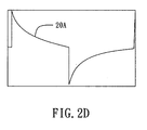
- FIG. 2D shows an enlarged view of waveform of an electronic signal read out by a pad corresponding to a pulse signal input by a specific pad when no touch point is present on the touch panel shown in FIG. 2B .
- FIG. 2E shows an enlarged view of waveform of an electronic signal read out by a pad corresponding to a pulse signal input by a specific pad when a touch point is present on the touch panel shown in FIG. 2B .
- FIG. 3A shows a touch point locating system of the touch panel of the second embodiment of the present disclosure.
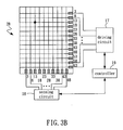
- FIG. 3B shows a schematic diagram of the combination of the first conductive film and the second conductive film shown in FIG. 3A .
- FIG. 3C shows the signal waveforms of the sensed electronic signals by any pad shown in FIG. 3B after touching.
- FIG. 3D shows an enlarged view of waveform of an electronic signal read out by a pad corresponding to a pulse signal input by a specific pad when no touch point is present on the touch panel.
- FIG. 3E shows an enlarged view of waveform of an electronic signal read out by a pad corresponding to a pulse signal input by a specific pad 140 when a touch point is present on the touch panel in FIG. 3B .
- FIG. 4A shows a method of locating a touch point on the touch panel of one embodiment of the present disclosure.
- FIG. 4B shows a flow chart of determining the coordinate of the touch point on the system shown in FIG. 2B .
- FIG. 4C shows a flow chart of determining the coordinate of the touch point on the system shown in FIG. 3B .
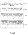
- FIG. 4D shows another flow chart of determining the coordinate of the touch point on the system shown in FIG. 3B .
- FIG. 5A shows a plurality of touch points selected along x-axis corresponding to the pad designated as 13.
- FIG. 5B shows a diagram drawn according to the values of the differences of the sensed electronic signals of a plurality of touch points selected along x-axis corresponding to the pad designated as 13.
- FIG. 1A shows an exploded view of a touch panel 1 of one embodiment of the present disclosure
- FIG. 1B shows a sectional view of the touch panel 1.
- the touch panel 1 includes, from bottom to top in sequence, a first insulating substrate 11, a first conductive film 12, an insulating layer 13, a second conductive film 14, and a second insulating substrate 15.
- the terms “bottom” and “top” only indicate relative position or direction.
- the term “top” indicates a direction toward the touch surface of the touch panel
- the term “bottom” indicates a direction away the touch surface of the touch panel.
- the second conductive film 14 is closer to the touch surface of the touch panel than the first conductive film 12.
- the first insulating substrate 11 is used as the bottom substrate, while the second insulating substrate 15 is used as the top substrate.
- the insulating layer 13 is between the first insulating substrate 11 and the second insulating substrate 15.
- the first conductive film 12 is between the first insulating substrate 11 and the insulating layer 13, and the second conductive film 14 is between the insulating layer 13 and the second insulating substrate 15.
- other additional layers can also be inserted into any two of the above-mentioned layers/films.
- first pads 120 are disposed on the peripheral region of the first conductive film 12 along a first direction such as x-axis or a transverse axis.
- Multiple second pads 140 are disposed on the peripheral region of the second conductive film 14 along a second direction such as y-axis or a longitudinal axis.
- the first direction is optionally perpendicular to the second direction, while the first direction is not limited to be perpendicular to the second direction in other embodiments.
- the materials of the first insulating substrate 11 and the second insulating substrate 15 are selected from one of the following materials or are combinations of portions of the following materials: Poly-Ethylene-Terephthalate ( PET ) , Polycarbonate ( PC ), Poly-Methyl-Meth-Acrylate ( PMMA ), Poly-Imide ( PI ) , and Poly-Ethylene ( PE ) .
- the material of the insulating layer 13 includes, but not limited to, glass or polymer material.
- the materials of the first pads 120 and the second pads 140 include conductors, such as metal.
- the first conductive film 12 and the second conductive film 14 include conductive films with anisotropic impedance, such as carbon nanotube ( CNT ) films, or etched or laser cut carbon nanotube films. A plurality of laser cutting lines on the carbon nanotube film resulting from the laser cutting process may not affect the original property of anisotropic impedance.
- the first conductive film 12 and the second conductive film 14 are CNT films without being etched or laser cut.
- the CNT films are formed by growing carbon nanotubes on a quartz substrate, a silicon substrate or a substrate of other materials through deposition processes such as a chemical vapor deposition (CVD ) process, then each carbon nanotube is extended out by an extension process.
- CVD chemical vapor deposition
- the CNT film has minimum impedance along the direction of extension and maximum impedance along the direction perpendicular to the direction of extension so as to have anisotropic impedance.
- FIG. 1C shows capacitors of the touch panel 1 formed at a touch point on the surface of the touch panel 1, while a first capacitor C1 is formed between the first conductive film 12 and the second conductive film 14, and a second capacitor C2 is formed between the second conductive film 14 and a stylus or a finger 16.
- the values of the first capacitor C1 and the second capacitor C2 may also be different.
- the structure of the touch panel 1 constitutes a capacitive-type touch panel.
- FIG. 2A shows a touch point locating system 2A of the touch panel of the first embodiment of the present disclosure.
- the impedance of the first conductive film 12 along the second direction such as y-axis or a longitudinal axis is minimum and relatively less than the impedance along other directions.
- the impedance of the second conductive film 14 along the first direction such as x-axis or a transverse axis is minimum and relatively less than the impedance along other directions.
- Each first pad 120 connects to an electronic signal input circuit or a driving circuit 17 via conductive lines.
- the driving circuit 17 inputs electronic signals with the same pulse waveform or other waveforms to each first pad 120 in sequence or simultaneously.
- Each second pad 140 connects to an electronic signal readout circuit or a sensing circuit 18 via conductive lines to read out sensed electronic signals of each second pad 140.
- the first pad 120 is used as the driving electronic signal pad, while the second pad 140 is used as the sensing electronic signal pad.
- the driving circuit 17 and the sensing circuit 18 are controlled by a controller 19.
- FIG. 2B shows a schematic diagram of the combination of the first conductive film 12 and the second conductive film 14.
- ten first pads 120 are shown and designated as 3, 8, 13, 18, 23, 28, 33, 38, 43, and 48
- thirteen second pads 140 are shown and designated as 3, 8, 13, 18, 23, 28, 33, 38, 43, 48, 53, 58 and 63.
- the capacitance values of the first capacitor C1 and the second capacitor C2 generate sensed electronic signals with specific features on the second pads 140 so as to determine the coordinate of the touch point on the surface of the touch panel 1 such as x coordinate of x-axis or a transverse axis and y coordinate of y-axis or a longitudinal axis.
- FIG. 3A shows a touch point locating system 2B of the touch panel of the second embodiment of the present disclosure.
- the impedance of the first conductive film 12 along the second direction such as y-axis or a longitudinal axis is minimum and relatively less than the impedance along other directions.
- the impedance of the second conductive film 14 along the first direction such as x-axis or a transverse axis is minimum and relatively less than the impedance along other directions.
- each second pad 140 connects to an electronic signal input circuit or a driving circuit 17 via conductive lines.
- the driving circuit 17 inputs electronic signals with the same pulse waveform or other waveforms to each first pad 140 in sequence or simultaneously.
- Each first pad 120 connects to an electronic signal readout circuit or a sensing circuit 18 via conductive lines to read out sensed electronic signals of each second pad 120.
- the second pad 140 is used as the driving electronic signal pad, while the first pad 120 is used as the sensing electronic signal pad.
- the driving circuit 17 and the sensing circuit 18 are controlled by a controller 19.
- FIG. 3B shows a schematic diagram of the combination of the first conductive film 12 and the second conductive film 14.
- ten first pads 120 are shown and designated as 3, 8, 13, 18, 23, 28, 33, 38, 43, and 48
- thirteen second pads 140 are shown and designated as 3, 8, 13, 18, 23, 28, 33, 38, 43, 48, 53, 58 and 63.
- the capacitance values of the first capacitor C1 and the second capacitor C2 generate sensed electronic signals with specific features on the second pads 120 so as to determine the coordinate of the touch point on the surface of the touch panel 1 such as x coordinate of x-axis or a transverse axis and y coordinate of y-axis or a longitudinal axis.
- FIG. 4A shows a method of locating a touch point on the touch panel of one embodiment of the present disclosure.
- step 31 electronic signals with the same pulse waveforms or other waveforms are input from the driving circuit 17 to each pad in sequence or simultaneously.
- the pad includes the first pad 120 shown in FIG. 2B or the second pad 140 shown in FIG. 3B .
- step 32 the sensed electronic signal of each pad is read out by the sensing circuit 18.
- the pad includes the second pad 140 shown in FIG. 2B or the first pad 120 shown in FIG. 3B .
- the location/position of the touch point on the surface of the touch panel 1 is determined by the controller 19 according to the sensed electronic signals.
- the first conductive film 12 is used as the bottom conductive film
- the second conductive film 14 is used as the top conductive film, such that the electronic signals are input to the bottom conductive film and the sensed electronic signals are generated from the top conductive film.
- the step 33 of determining the location/position of the touch point on the surface of the touch panel 1 includes steps 331A and 332A shown in FIG. 4B .
- step 331A the coordinate of the touch point along the second direction or y-axis or the longitudinal axis is obtained through locating the coordinate or position of the pad such as the second pad 140 designated as 13 sensing the electronic signal with a maximum variation of waveform amplitude by comparing before touching with after touching.
- step 332A the coordinate of the touch point along the first direction or x-axis or the transverse axis is obtained through locating the coordinate or position of the pad such as the first pad 120 corresponding to the maximum variation of the waveform amplitude by comparing the signal waveforms of the sensed electronic signals of the second pad 140 designated as 13 shown in FIG. 2C before touching with after touching.
- each first pad 120 When the waveform of the electronic signal received by each first pad 120 is pulse waveform, the waveform of the electronic signal sensed by each second pad 140 is shown in FIG. 2C if there is only one touch point. As shown in FIG. 2C , the sections of the waveform from left to right are generated from the pulse signals input by the ten first pads 120 designated from 3 to 48.
- FIG. 2D shows an enlarged view of waveform 20A of an electronic signal sensed by the second pad 140 corresponding to a pulse signal input by a first pad 120 when no touch point is present on the touch panel.
- FIG. 2E shows an enlarged view of waveform 21A of an electronic signal sensed by the second pad 140 such as the second pad designated as 13 corresponding to a pulse signal input by a first pad 120 when a touch point is present on the touch panel.
- a maximum variation between waveform 21A of the sensed electronic signal sensed by the second pad 140 designated as 13 after touching and waveform 20A of the sensed electronic signal sensed by the same pad before touching is present when a stylus or a finger touch the touch point on the surface of the touch panel shown in FIG. 2B .
- the coordinate of the touch point along the second direction or y-axis or the longitudinal axis is obtained by the step 331A, and the coordinate of the touch point along the first direction or x-axis or the transverse axis is obtained via the step 332A.
- the first conductive film 12 is used as the bottom conductive film
- the second conductive film 14 is used as the top conductive film, such that the electronic signals are input to the top conductive film and the sensed electronic signals are generated from the bottom conductive film.
- the step 33 of determining the location/position of the touch point on the surface of the touch panel 1 includes steps 331B and 332B shown in FIG. 4C .
- step 331B the coordinate of the touch point along the second direction or y-axis or the longitudinal axis is obtained through locating the coordinate or position of the pad such as the second pad 140 corresponding to a minimum amplitude of signal waveform of the sensed electronic signals resulting from touching.
- the step 332B is used to obtain the coordinate of the touch point along the first direction or x-axis or the transverse axis.
- each second pad 140 When the waveform of the electronic signal received by each second pad 140 is pulse waveform, the waveform of the sensed electronic signal sensed by each first pad 120 is shown in FIG. 3C if there is only one touch point. As shown in FIG. 3C , the sections of the waveform from left to right are generated from the pulse signals input by the thirteen second pads 140 designated from 3 to 63.
- FIG. 3D shows an enlarged view of waveform 20B of an electronic signal sensed by the first pad 120 corresponding to a pulse signal input by the second pad 140 when no touch point is present on the touch panel.
- FIG. 3E shows an enlarged view of waveform 21B of an electronic signal sensed by the first pad 120 such as the first pad designated as 13 corresponding to a pulse signal input by the second pad 140 when a touch point is present on the touch panel.
- a maximum variation between waveform 21B of the sensed electronic signal sensed by the first pad 120 designated as 13 after touching and waveform 20B of the electronic signal sensed by the same pad before touching is present when a stylus or a finger touch the touch point on the surface of the touch panel shown in FIG. 3B .
- the variation between the waveform 21B of the electronic signal after touching and the waveform 20B of the electronic signal before touching is susceptible to RC delay and is not precise, the detection or determination of the coordinate of the touch point along the first direction or x-axis or the transverse axis can not solely rely on the variation between the waveform 21B and the waveform 20B.
- the coordinate of the touch point along the second direction or y-axis or the longitudinal axis is obtained through comparing the signal waveforms of the sensed electronic signals read out by the first pads 120 to locate the coordinate or position of the second pad 140 designated as 13 which inputs the electronic signal causing the minimum amplitude of signal waveform.
- the coordinate of the touch point along the second direction or y-axis or the longitudinal axis according to step 331B is obtained through locating the coordinate or position of the pad corresponding to the minimum amplitude of signal waveform of the sensed electronic signals by comparing before touching with after touching.
- the coordinate of the touch point along the first direction or x-axis or the transverse axis according to step 332B is obtained through locating the coordinate or position of the pad such as the first pad 120 designated as 13 corresponding to a maximum variation of signal waveform of the sensed electronic signals by comparing the signal waveforms of the sensed electronic signals before touching with after touching.
- FIG. 4D shows another embodiment of step 33 of the method of locating a touch point on the touch panel.
- the step 331C of determining the coordinate of the touch point along the second direction or y-axis or the longitudinal axis is similar to the step 331B.
- the coordinate of the touch point along the second direction or y-axis or the longitudinal axis is obtained through locating the coordinate or position of the pad such as the second pad 140 designated as 13.
- a plurality of points are selected along the first direction or x-axis or the transverse axis corresponding to the coordinate of the second direction or y-axis or the longitudinal axis.
- the x-axis coordinates of these points are the x-axis coordinates of the first pads 120 designated as 3, 8, 13, 28 and 43.
- step 333C the differences of the sensed electronic signals of the first pads 120 of the points before touching with after touching corresponding to the coordinate of the second pad 140 respectively are calculated and stored, and the unit of the differences of the sensed electronic signals is millivolt (mv).
- step 334C the x-axis coordinate of the unknown touch point is obtained by the differences of the sensed electronic signals stored in step 333C and the difference of the sensed electronic signal of the unknown touch point calculated by comparing before touching with after touching.
- Table 1 shows an example of numerical values of the electronic signal, and the coordinates along the first direction or x-axis or the transverse axis and the coordinates along the second direction or y-axis or the longitudinal axis are respectively shown by the designated numbers of the first pads 120 used as sensing and the second pads 140 used as driving respectively.
- the values in Table 1 can be used to draw FIG.5B .
- the longitudinal axis represents the differences of the electronic signals before touching with after touching sensed by the pads, while the transverse axis represents the coordinates along the first direction or x-axis.
- the values of Table 1 or FIG.5B can be previously stored, or can be generated by the touching of an user before using the touch panel.
- the coordinates along the second direction or y-axis or the longitudinal axis are obtained through step 331C
- the coordinates along the first direction or x-axis or the transverse axis are also obtained through the corresponding values of the differences of the sensed electronic signals of Table 1 or FIG.5 B .
Landscapes
- Engineering & Computer Science (AREA)
- General Engineering & Computer Science (AREA)
- Theoretical Computer Science (AREA)
- Human Computer Interaction (AREA)
- Physics & Mathematics (AREA)
- General Physics & Mathematics (AREA)
- Position Input By Displaying (AREA)
Applications Claiming Priority (1)
| Application Number | Priority Date | Filing Date | Title |
|---|---|---|---|
| CN2009103061152A CN101995990B (zh) | 2009-08-26 | 2009-08-26 | 触控面板及触控面板的触碰点定位方法 |
Publications (2)
| Publication Number | Publication Date |
|---|---|
| EP2290511A2 true EP2290511A2 (fr) | 2011-03-02 |
| EP2290511A3 EP2290511A3 (fr) | 2012-10-31 |
Family
ID=43216507
Family Applications (1)
| Application Number | Title | Priority Date | Filing Date |
|---|---|---|---|
| EP10173916A Withdrawn EP2290511A3 (fr) | 2009-08-26 | 2010-08-24 | Panneau tactile et procédé de localisation d'un point touché sur celui-ci |
Country Status (5)
| Country | Link |
|---|---|
| US (1) | US8681118B2 (fr) |
| EP (1) | EP2290511A3 (fr) |
| JP (1) | JP5697923B2 (fr) |
| KR (1) | KR20110021649A (fr) |
| CN (1) | CN101995990B (fr) |
Cited By (2)
| Publication number | Priority date | Publication date | Assignee | Title |
|---|---|---|---|---|
| US11901629B2 (en) | 2021-09-30 | 2024-02-13 | Eagle Technology, Llc | Deployable antenna reflector |
| US11949161B2 (en) | 2021-08-27 | 2024-04-02 | Eagle Technology, Llc | Systems and methods for making articles comprising a carbon nanotube material |
Families Citing this family (16)
| Publication number | Priority date | Publication date | Assignee | Title |
|---|---|---|---|---|
| FR2968103B1 (fr) * | 2010-11-26 | 2013-04-26 | Stantum | Capteur tactile transparent et procédé de fabrication associe |
| TWI450168B (zh) * | 2011-07-12 | 2014-08-21 | Shih Hua Technology Ltd | 觸控面板 |
| TWI465796B (zh) * | 2011-09-01 | 2014-12-21 | Shih Hua Technology Ltd | 觸摸屏面板 |
| CN102981655A (zh) * | 2011-09-02 | 2013-03-20 | 天津富纳源创科技有限公司 | 触摸屏面板 |
| CN102999193B (zh) * | 2011-09-13 | 2016-01-13 | 天津富纳源创科技有限公司 | 触摸屏触摸点之检测方法 |
| CN103135864B (zh) * | 2011-11-28 | 2016-05-18 | 天津富纳源创科技有限公司 | 电容式触控面板以及防止其漏电流的驱动方法 |
| CN102419655B (zh) * | 2011-12-09 | 2013-11-20 | 天津富纳源创科技有限公司 | 触摸屏面板 |
| TWI436411B (zh) * | 2012-04-27 | 2014-05-01 | Liu Hung Ta | 觸控裝置 |
| US8698778B2 (en) * | 2012-07-30 | 2014-04-15 | Olympus Ndt | Method of manipulating impedance plane with a multi-point touch on touch screen |
| CN103631413A (zh) * | 2012-08-24 | 2014-03-12 | 天津富纳源创科技有限公司 | 触摸屏及触控显示装置 |
| CN103631414A (zh) * | 2012-08-24 | 2014-03-12 | 天津富纳源创科技有限公司 | 触摸屏 |
| CN103631415A (zh) * | 2012-08-24 | 2014-03-12 | 天津富纳源创科技有限公司 | 触摸屏及触控显示装置 |
| CN103926978A (zh) * | 2013-01-15 | 2014-07-16 | 识骅科技股份有限公司 | 便携式电脑 |
| CN104423742A (zh) * | 2013-09-02 | 2015-03-18 | 天津富纳源创科技有限公司 | 触摸屏及其制备方法 |
| CN104423744A (zh) * | 2013-09-02 | 2015-03-18 | 天津富纳源创科技有限公司 | 触摸屏及其制备方法 |
| CN113407069A (zh) * | 2020-03-17 | 2021-09-17 | 高尔科技股份有限公司 | 红外线热反应式控制面板 |
Family Cites Families (19)
| Publication number | Priority date | Publication date | Assignee | Title |
|---|---|---|---|---|
| JP3061115B2 (ja) * | 1996-11-15 | 2000-07-10 | アルプス電気株式会社 | 電荷電流検出回路およびこれを利用した座標入力装置 |
| US7663607B2 (en) * | 2004-05-06 | 2010-02-16 | Apple Inc. | Multipoint touchscreen |
| JP2002365427A (ja) * | 2001-06-04 | 2002-12-18 | Toray Ind Inc | 偏光子およびその製造方法 |
| KR100469358B1 (ko) * | 2002-12-23 | 2005-02-02 | 엘지.필립스 엘시디 주식회사 | 터치 패널의 구동 방법 |
| US20050209392A1 (en) * | 2003-12-17 | 2005-09-22 | Jiazhong Luo | Polymer binders for flexible and transparent conductive coatings containing carbon nanotubes |
| US8603611B2 (en) * | 2005-05-26 | 2013-12-10 | Gunze Limited | Transparent planar body and transparent touch switch |
| JP2008134836A (ja) * | 2006-11-28 | 2008-06-12 | Wacom Co Ltd | タッチパネル装置 |
| JP4998919B2 (ja) * | 2007-06-14 | 2012-08-15 | ソニーモバイルディスプレイ株式会社 | 静電容量型入力装置 |
| US8212792B2 (en) * | 2007-08-14 | 2012-07-03 | Tyco Electronics Corporation | Touchscreen using oriented microscopic linear conductive elements |
| CN101470560B (zh) * | 2007-12-27 | 2012-01-25 | 清华大学 | 触摸屏及显示装置 |
| CN101470559B (zh) * | 2007-12-27 | 2012-11-21 | 清华大学 | 触摸屏及显示装置 |
| EP2053495A3 (fr) * | 2007-10-23 | 2011-04-27 | Tsinghua University | Écran tactile, son procédé de fabrication, et dispositif d'affichage l'utilisant |
| EP2071438A3 (fr) * | 2007-12-14 | 2011-04-27 | Tsing Hua University | Écran tactile et dispositif d'affichage l'utilisant |
| CN101470565B (zh) * | 2007-12-27 | 2011-08-24 | 清华大学 | 触摸屏及显示装置 |
| EP2073109A3 (fr) * | 2007-12-21 | 2012-08-22 | Tsing Hua University | Écran tactile et dispositif d'affichage l'utilisant |
| CN201222242Y (zh) * | 2008-06-11 | 2009-04-15 | 深圳市德普特光电显示技术有限公司 | 电容式触摸屏 |
| CN201218887Y (zh) * | 2008-06-17 | 2009-04-08 | 宸鸿光电科技股份有限公司 | 电容式触控显示面板 |
| CN101303635A (zh) * | 2008-07-01 | 2008-11-12 | 友达光电股份有限公司 | 电容式触控面板及其制作方法 |
| CN101950231B (zh) * | 2009-07-10 | 2012-10-24 | 群康科技(深圳)有限公司 | 用于触控装置的侦测触碰位置的方法 |
-
2009
- 2009-08-26 CN CN2009103061152A patent/CN101995990B/zh active Active
-
2010
- 2010-07-21 US US12/840,302 patent/US8681118B2/en not_active Expired - Fee Related
- 2010-07-30 KR KR1020100074037A patent/KR20110021649A/ko not_active Withdrawn
- 2010-08-24 EP EP10173916A patent/EP2290511A3/fr not_active Withdrawn
- 2010-08-25 JP JP2010188261A patent/JP5697923B2/ja active Active
Non-Patent Citations (1)
| Title |
|---|
| None |
Cited By (2)
| Publication number | Priority date | Publication date | Assignee | Title |
|---|---|---|---|---|
| US11949161B2 (en) | 2021-08-27 | 2024-04-02 | Eagle Technology, Llc | Systems and methods for making articles comprising a carbon nanotube material |
| US11901629B2 (en) | 2021-09-30 | 2024-02-13 | Eagle Technology, Llc | Deployable antenna reflector |
Also Published As
| Publication number | Publication date |
|---|---|
| CN101995990B (zh) | 2013-01-09 |
| US20110050627A1 (en) | 2011-03-03 |
| EP2290511A3 (fr) | 2012-10-31 |
| CN101995990A (zh) | 2011-03-30 |
| US8681118B2 (en) | 2014-03-25 |
| JP2011048827A (ja) | 2011-03-10 |
| JP5697923B2 (ja) | 2015-04-08 |
| KR20110021649A (ko) | 2011-03-04 |
Similar Documents
| Publication | Publication Date | Title |
|---|---|---|
| EP2290511A2 (fr) | Panneau tactile et procédé de localisation d'un point touché sur celui-ci | |
| KR101661786B1 (ko) | 곡선형 표면 위의 터치 감지 방법 | |
| KR101702676B1 (ko) | 곡선형 표면 위의 터치 감지 방법 | |
| US9921696B2 (en) | Sensor with diffusing resistor | |
| EP2278443B1 (fr) | Procédé de détection d'effleurements multiples pour panneau tactile | |
| US20140168171A1 (en) | Touch sensing device and touch sensing method | |
| TWI506520B (zh) | 電容式觸控裝置的控制方法 | |
| TWI441048B (zh) | 觸控面板及觸碰點定位方法 | |
| US9547030B2 (en) | Method of recognizing touch | |
| US20140160057A1 (en) | Touch sensing method and touch sensing apparatus | |
| US20170205931A1 (en) | Touch Module, Touch Screen Panel, Touch Positioning Method Thereof and Display Device | |
| US9098157B2 (en) | Touch sensing apparatus | |
| US9240782B2 (en) | One-dimensional capacitive touch panel with stable coupling capacitance | |
| TW201229850A (en) | Touch-sensitive coordinate input apparatus, touch panel and electronic devices having the same | |
| US20130155003A1 (en) | Touch sensing apparatus and method thereof | |
| US9329740B2 (en) | Method of recognizing touch | |
| EP3158423A1 (fr) | Panneau tactile capacitif ayant des structures diélectriques formées en son sein | |
| US20140062915A1 (en) | Touchscreen panel and touchscreen device | |
| Rappaport et al. | 96‐4: Invited Paper: Surface Dial: Enabling Tangible Dual‐handed Interactions on Capacitive Touchscreens | |
| Cairns et al. | Interacting with Flexible Displays | |
| KR20190047850A (ko) | 디지타이저 및 이를 포함하는 표시 장치 | |
| HK1163860B (en) | Detecting touch on a curved surface | |
| HK1163860A (en) | Detecting touch on a curved surface |
Legal Events
| Date | Code | Title | Description |
|---|---|---|---|
| PUAI | Public reference made under article 153(3) epc to a published international application that has entered the european phase |
Free format text: ORIGINAL CODE: 0009012 |
|
| AK | Designated contracting states |
Kind code of ref document: A2 Designated state(s): AL AT BE BG CH CY CZ DE DK EE ES FI FR GB GR HR HU IE IS IT LI LT LU LV MC MK MT NL NO PL PT RO SE SI SK SM TR |
|
| AX | Request for extension of the european patent |
Extension state: BA ME RS |
|
| PUAL | Search report despatched |
Free format text: ORIGINAL CODE: 0009013 |
|
| AK | Designated contracting states |
Kind code of ref document: A3 Designated state(s): AL AT BE BG CH CY CZ DE DK EE ES FI FR GB GR HR HU IE IS IT LI LT LU LV MC MK MT NL NO PL PT RO SE SI SK SM TR |
|
| AX | Request for extension of the european patent |
Extension state: BA ME RS |
|
| RIC1 | Information provided on ipc code assigned before grant |
Ipc: G06F 3/044 20060101AFI20120921BHEP |
|
| 17P | Request for examination filed |
Effective date: 20130429 |
|
| 17Q | First examination report despatched |
Effective date: 20160621 |
|
| STAA | Information on the status of an ep patent application or granted ep patent |
Free format text: STATUS: EXAMINATION IS IN PROGRESS |
|
| RAP1 | Party data changed (applicant data changed or rights of an application transferred) |
Owner name: INNOLUX CORPORATION |
|
| STAA | Information on the status of an ep patent application or granted ep patent |
Free format text: STATUS: THE APPLICATION IS DEEMED TO BE WITHDRAWN |
|
| 18D | Application deemed to be withdrawn |
Effective date: 20170725 |