EP2290590A2 - Support de données portatif - Google Patents
Support de données portatif Download PDFInfo
- Publication number
- EP2290590A2 EP2290590A2 EP10008397A EP10008397A EP2290590A2 EP 2290590 A2 EP2290590 A2 EP 2290590A2 EP 10008397 A EP10008397 A EP 10008397A EP 10008397 A EP10008397 A EP 10008397A EP 2290590 A2 EP2290590 A2 EP 2290590A2
- Authority
- EP
- European Patent Office
- Prior art keywords
- module
- data carrier
- contact device
- electrically conductive
- elastic
- Prior art date
- Legal status (The legal status is an assumption and is not a legal conclusion. Google has not performed a legal analysis and makes no representation as to the accuracy of the status listed.)
- Granted
Links
Images


Classifications
-
- G—PHYSICS
- G06—COMPUTING OR CALCULATING; COUNTING
- G06K—GRAPHICAL DATA READING; PRESENTATION OF DATA; RECORD CARRIERS; HANDLING RECORD CARRIERS
- G06K19/00—Record carriers for use with machines and with at least a part designed to carry digital markings
- G06K19/06—Record carriers for use with machines and with at least a part designed to carry digital markings characterised by the kind of the digital marking, e.g. shape, nature, code
- G06K19/067—Record carriers with conductive marks, printed circuits or semiconductor circuit elements, e.g. credit or identity cards also with resonating or responding marks without active components
- G06K19/07—Record carriers with conductive marks, printed circuits or semiconductor circuit elements, e.g. credit or identity cards also with resonating or responding marks without active components with integrated circuit chips
- G06K19/077—Constructional details, e.g. mounting of circuits in the carrier
- G06K19/07745—Mounting details of integrated circuit chips
-
- G—PHYSICS
- G06—COMPUTING OR CALCULATING; COUNTING
- G06K—GRAPHICAL DATA READING; PRESENTATION OF DATA; RECORD CARRIERS; HANDLING RECORD CARRIERS
- G06K19/00—Record carriers for use with machines and with at least a part designed to carry digital markings
- G06K19/06—Record carriers for use with machines and with at least a part designed to carry digital markings characterised by the kind of the digital marking, e.g. shape, nature, code
- G06K19/067—Record carriers with conductive marks, printed circuits or semiconductor circuit elements, e.g. credit or identity cards also with resonating or responding marks without active components
- G06K19/07—Record carriers with conductive marks, printed circuits or semiconductor circuit elements, e.g. credit or identity cards also with resonating or responding marks without active components with integrated circuit chips
- G06K19/077—Constructional details, e.g. mounting of circuits in the carrier
- G06K19/07749—Constructional details, e.g. mounting of circuits in the carrier the record carrier being capable of non-contact communication, e.g. constructional details of the antenna of a non-contact smart card
-
- G—PHYSICS
- G06—COMPUTING OR CALCULATING; COUNTING
- G06K—GRAPHICAL DATA READING; PRESENTATION OF DATA; RECORD CARRIERS; HANDLING RECORD CARRIERS
- G06K19/00—Record carriers for use with machines and with at least a part designed to carry digital markings
- G06K19/06—Record carriers for use with machines and with at least a part designed to carry digital markings characterised by the kind of the digital marking, e.g. shape, nature, code
- G06K19/067—Record carriers with conductive marks, printed circuits or semiconductor circuit elements, e.g. credit or identity cards also with resonating or responding marks without active components
- G06K19/07—Record carriers with conductive marks, printed circuits or semiconductor circuit elements, e.g. credit or identity cards also with resonating or responding marks without active components with integrated circuit chips
- G06K19/077—Constructional details, e.g. mounting of circuits in the carrier
- G06K19/07749—Constructional details, e.g. mounting of circuits in the carrier the record carrier being capable of non-contact communication, e.g. constructional details of the antenna of a non-contact smart card
- G06K19/0775—Constructional details, e.g. mounting of circuits in the carrier the record carrier being capable of non-contact communication, e.g. constructional details of the antenna of a non-contact smart card arrangements for connecting the integrated circuit to the antenna
-
- H—ELECTRICITY
- H05—ELECTRIC TECHNIQUES NOT OTHERWISE PROVIDED FOR
- H05K—PRINTED CIRCUITS; CASINGS OR CONSTRUCTIONAL DETAILS OF ELECTRIC APPARATUS; MANUFACTURE OF ASSEMBLAGES OF ELECTRICAL COMPONENTS
- H05K3/00—Apparatus or processes for manufacturing printed circuits
- H05K3/30—Assembling printed circuits with electric components, e.g. with resistors
- H05K3/32—Assembling printed circuits with electric components, e.g. with resistors electrically connecting electric components or wires to printed circuits
- H05K3/325—Assembling printed circuits with electric components, e.g. with resistors electrically connecting electric components or wires to printed circuits by abutting or pinching; Mechanical auxiliary parts therefor
- H05K3/326—Assembling printed circuits with electric components, e.g. with resistors electrically connecting electric components or wires to printed circuits by abutting or pinching; Mechanical auxiliary parts therefor the printed circuit having integral resilient or deformable parts, e.g. tabs or parts of flexible circuits
-
- H—ELECTRICITY
- H10—SEMICONDUCTOR DEVICES; ELECTRIC SOLID-STATE DEVICES NOT OTHERWISE PROVIDED FOR
- H10W—GENERIC PACKAGES, INTERCONNECTIONS, CONNECTORS OR OTHER CONSTRUCTIONAL DETAILS OF DEVICES COVERED BY CLASS H10
- H10W70/00—Package substrates; Interposers; Redistribution layers [RDL]
- H10W70/60—Insulating or insulated package substrates; Interposers; Redistribution layers
- H10W70/67—Insulating or insulated package substrates; Interposers; Redistribution layers characterised by their insulating layers or insulating parts
- H10W70/68—Shapes or dispositions thereof
-
- H—ELECTRICITY
- H10—SEMICONDUCTOR DEVICES; ELECTRIC SOLID-STATE DEVICES NOT OTHERWISE PROVIDED FOR
- H10W—GENERIC PACKAGES, INTERCONNECTIONS, CONNECTORS OR OTHER CONSTRUCTIONAL DETAILS OF DEVICES COVERED BY CLASS H10
- H10W70/00—Package substrates; Interposers; Redistribution layers [RDL]
- H10W70/60—Insulating or insulated package substrates; Interposers; Redistribution layers
- H10W70/699—Insulating or insulated package substrates; Interposers; Redistribution layers for flat cards, e.g. credit cards
-
- H—ELECTRICITY
- H05—ELECTRIC TECHNIQUES NOT OTHERWISE PROVIDED FOR
- H05K—PRINTED CIRCUITS; CASINGS OR CONSTRUCTIONAL DETAILS OF ELECTRIC APPARATUS; MANUFACTURE OF ASSEMBLAGES OF ELECTRICAL COMPONENTS
- H05K1/00—Printed circuits
- H05K1/18—Printed circuits structurally associated with non-printed electric components
- H05K1/182—Printed circuits structurally associated with non-printed electric components associated with components mounted in printed circuit boards [PCB], e.g. insert-mounted components [IMC]
- H05K1/183—Printed circuits structurally associated with non-printed electric components associated with components mounted in printed circuit boards [PCB], e.g. insert-mounted components [IMC] associated with components mounted in and supported by recessed areas of the PCBs
-
- H—ELECTRICITY
- H05—ELECTRIC TECHNIQUES NOT OTHERWISE PROVIDED FOR
- H05K—PRINTED CIRCUITS; CASINGS OR CONSTRUCTIONAL DETAILS OF ELECTRIC APPARATUS; MANUFACTURE OF ASSEMBLAGES OF ELECTRICAL COMPONENTS
- H05K2201/00—Indexing scheme relating to printed circuits covered by H05K1/00
- H05K2201/03—Conductive materials
- H05K2201/0302—Properties and characteristics in general
- H05K2201/0314—Elastomeric connector or conductor, e.g. rubber with metallic filler
-
- H—ELECTRICITY
- H05—ELECTRIC TECHNIQUES NOT OTHERWISE PROVIDED FOR
- H05K—PRINTED CIRCUITS; CASINGS OR CONSTRUCTIONAL DETAILS OF ELECTRIC APPARATUS; MANUFACTURE OF ASSEMBLAGES OF ELECTRICAL COMPONENTS
- H05K2201/00—Indexing scheme relating to printed circuits covered by H05K1/00
- H05K2201/03—Conductive materials
- H05K2201/0332—Structure of the conductor
- H05K2201/0364—Conductor shape
- H05K2201/0367—Metallic bump or raised conductor not used as solder bump
-
- H—ELECTRICITY
- H05—ELECTRIC TECHNIQUES NOT OTHERWISE PROVIDED FOR
- H05K—PRINTED CIRCUITS; CASINGS OR CONSTRUCTIONAL DETAILS OF ELECTRIC APPARATUS; MANUFACTURE OF ASSEMBLAGES OF ELECTRICAL COMPONENTS
- H05K2201/00—Indexing scheme relating to printed circuits covered by H05K1/00
- H05K2201/09—Shape and layout
- H05K2201/09209—Shape and layout details of conductors
- H05K2201/09372—Pads and lands
- H05K2201/09472—Recessed pad for surface mounting; Recessed electrode of component
-
- H—ELECTRICITY
- H05—ELECTRIC TECHNIQUES NOT OTHERWISE PROVIDED FOR
- H05K—PRINTED CIRCUITS; CASINGS OR CONSTRUCTIONAL DETAILS OF ELECTRIC APPARATUS; MANUFACTURE OF ASSEMBLAGES OF ELECTRICAL COMPONENTS
- H05K2201/00—Indexing scheme relating to printed circuits covered by H05K1/00
- H05K2201/09—Shape and layout
- H05K2201/09209—Shape and layout details of conductors
- H05K2201/09654—Shape and layout details of conductors covering at least two types of conductors provided for in H05K2201/09218 - H05K2201/095
- H05K2201/0969—Apertured conductors
-
- H—ELECTRICITY
- H05—ELECTRIC TECHNIQUES NOT OTHERWISE PROVIDED FOR
- H05K—PRINTED CIRCUITS; CASINGS OR CONSTRUCTIONAL DETAILS OF ELECTRIC APPARATUS; MANUFACTURE OF ASSEMBLAGES OF ELECTRICAL COMPONENTS
- H05K2201/00—Indexing scheme relating to printed circuits covered by H05K1/00
- H05K2201/10—Details of components or other objects attached to or integrated in a printed circuit board
- H05K2201/10613—Details of electrical connections of non-printed components, e.g. special leads
- H05K2201/10621—Components characterised by their electrical contacts
- H05K2201/10727—Leadless chip carrier [LCC], e.g. chip-modules for cards
-
- H—ELECTRICITY
- H05—ELECTRIC TECHNIQUES NOT OTHERWISE PROVIDED FOR
- H05K—PRINTED CIRCUITS; CASINGS OR CONSTRUCTIONAL DETAILS OF ELECTRIC APPARATUS; MANUFACTURE OF ASSEMBLAGES OF ELECTRICAL COMPONENTS
- H05K3/00—Apparatus or processes for manufacturing printed circuits
- H05K3/30—Assembling printed circuits with electric components, e.g. with resistors
- H05K3/303—Assembling printed circuits with electric components, e.g. with resistors with surface mounted components
- H05K3/305—Affixing by adhesive
-
- H—ELECTRICITY
- H05—ELECTRIC TECHNIQUES NOT OTHERWISE PROVIDED FOR
- H05K—PRINTED CIRCUITS; CASINGS OR CONSTRUCTIONAL DETAILS OF ELECTRIC APPARATUS; MANUFACTURE OF ASSEMBLAGES OF ELECTRICAL COMPONENTS
- H05K3/00—Apparatus or processes for manufacturing printed circuits
- H05K3/40—Forming printed elements for providing electric connections to or between printed circuits
- H05K3/4007—Surface contacts, e.g. bumps
Definitions
- the present invention relates to a portable data carrier with an electronic module embedded in a data carrier body of the data carrier, a corresponding module, a data carrier body, an electrically conductive material for connecting the module to an electrical component of the data carrier body, and a method for producing such a data carrier.
- a smart card has a card body and an integrated circuit embedded in the card body.
- the integrated circuit is first packaged in a chip module in a variety of manufacturing processes and then the chip module is installed in the card body. As a rule, the chip module is glued into a recess of the card body.
- Communication with the integrated circuit can be carried out via a contact field of the chip card, which is contacted by a contacting unit for this purpose.
- the contact field is usually part of the chip module.
- a contactless communication may be provided.
- the card body may have an antenna coil, which is electrically connected to the integrated circuit during installation of the chip module.
- the card body may have, in addition to the antenna coil, other or further electrical components which are electrically connected to the integrated circuit during installation of the chip module.
- an electrically conductive contact between a contact device of an electrical component of the data carrier body, for example an antenna coil, and a contact device of an electronic module, for example a chip module is produced by frictionally interconnecting the respective contact devices by means of interlocking arrangements.
- the module is pressed into the disk body such that the corresponding contact devices, which are each formed as smooth surfaces, are pressed against each other.
- the respective contact devices are connected to one another by an integral material, which in each case comprises a material applied to the two contact devices.
- the contact device of the module as an electrically conductive band is formed, which contact by means of tapered elevations, which penetrate an electrically insulating layer, the contact means of the electrical component of the data carrier body.
- DE 10 2005 002 732 A1 as well as the DE 10 2005 002 728 A1 teach to connect the contact means of the electrical component of the data carrier with the contact device of the electronic module, which are each formed differently electrically conductive by means of a conductive material, preferably by means of a solder or a thermosetting conductive adhesive, whereby the two contact means are materially interconnected.
- connection between the two contact devices have the disadvantage that such a frictionally or cohesively produced connection can be easily interrupted due to the strong mechanical stresses on the disk when the module relative to the disk body if only slightly, shifts. Immediately contacted contact devices can lose contact, break up cohesive connections.
- an elastic, electrically conductive material is used for connecting the module to the component of the data carrier, the material being compressed when embedding the module in the data carrier body by the contact device of the electrical module of the data carrier body and the contact device of the module.
- Object of the present invention is to produce a further improved, acting on the disk body mechanical loads resistive electrically conductive connection between an electrical component of a data carrier body and embedded in the disk body module in a simple manner.
- An inventive data carrier comprises a data carrier body with an electrical component and an electronic module which is at least partially embedded in the data carrier body and electrically connected via a module contact device of the module by means of an elastic, electrically conductive material under pressure with a component contact device of the electrical component of the data carrier is.
- the module contact device is spatially structured and formed in the elastic, electrically conductive material is a spatial structure impressed by the spatially structured module contact device.
- An inventive electronic module is suitable to be at least partially embedded in a data carrier body of a portable data carrier and comprises a module contact device for electrically conductive connection of the module with an elastic, electrically conductive material of the data carrier.
- the module contact device is structured in such a way that it is suitable for impressing a spatial structure into the elastic, electrically conductive material when the module is embedded in the data carrier body under pressure.
- An elastic, electrically conductive material according to the invention is suitable for electrically conductive connection of an electronic module and an electrical component of a portable data carrier during at least partial embedding of the module in a data carrier body of the data carrier.
- the material according to the invention is designed such that upon embedding of the module in the data carrier body by the spatial structuring of the module contact device under pressure, a spatial structure is impressed into the material.
- An inventive data carrier body with an electrical component is therefore suitable for producing a data carrier according to the invention by at least partially embedding a module according to the invention and electrically connecting the module contact device of the module with a component contact device of the electrical component by means of an elastic, electrically conductive material according to the invention under pressure of the material through the module contact device ,
- a corresponding data carrier body with an electrical component, an electronic module and an elastic, electrically conductive material are provided in a first step. Thereafter, the material is arranged in a recess of the data carrier body such that the material is electrically conductively connected to a component contact device of the electrical component of the data carrier body.
- the module is at least partially embedded in the data carrier body such that the material electrically conductively connects the component contact device and a module contact device of the module under pressure.
- the module contact device is structured in a spatially structured manner and the material is embossed in a spatially structured manner when the module is embedded by the module contact device.
- the module contact device is formed spatially structured and when embedding the module in the disk body a corresponding spatial structure is embossed in the thus arranged electrically conductive material, the electrically conductive connection established between the module and the electrical component of the disk body can be provided even more fail-safe ,
- the structure in the material on the one hand and the structured contact surface of the module contact device on the other hand remains an electrically conductive contact between the module contact device and the material even with displacement of the module against the disk body due to a mechanical stress on the disk body, such as a bend of the same, longer as if the contact surface of the module contact device were formed flat.
- Both horizontal, in particular but vertical displacements of the module relative to the disk body lead so late, ie with very strong displacement of the module, to an interruption of the electrically conductive connection of the module and electrical component.
- This is due to the fact that the elastic material and the spatially structured contact surface of the module contact device pressed into it are in engagement due to the elasticity of the material and the structuring of the contact surface, which only dissolves gradually as the material of the module contact device is relieved of pressure. In this way, the electrically conductive connection is stable for a maximum of a long time even under heavy mechanical stress on the disk.
- the preparation of the data carrier can be done in a known, simple manner by embedding the module in the disk body. Due to the resulting pressurization of the material through the spatially structured module contact device, the material is automatically embossed accordingly.
- Known manufacturing methods therefore only have to be adapted with regard to the production of the spatially structured contact surface of the module contact device and with respect to the provision of a suitable elastic, electrically conductive material which can be impressed by the structured module contact device. All other production steps can remain unchanged.
- the elastic, electrically conductive material is designed in such a way that the spatial structure embossed by the spatially structured module contact device essentially remains intact in the material even when the pressure of the material decreases.
- the contact between the electrical component and the module via the electrically conductive material even at a strong vertical displacement of the module relative to the disk body are obtained, as long as the module contact device moves vertically along a flank of the embossing of the material, even if the elasticity of the material no longer allows vertical expansion of the material more.
- a greater vertical displacement of the module without interruption of contact can be ensured here.
- the displacement can be greater in the vertical direction by a depth of the embossed, maintained with decreasing pressurization spatial structure of the material larger than when using a flat contact surface without the contact stops.
- the module contact device is formed at least partially planar and a when embedding the module in the disk body the elastic, electrically conductive material or embedded module in the disk body of the component contact facing the contact surface of the module contact device is spatially structured by recesses, in particular grooves, holes or the like.
- the recesses may have the same or different depths and be arranged as a pattern, for example as a waffle pattern, or randomly.
- the flanks of the recesses can take any suitable angle to the module contact device.
- At least some of the recesses taper when embedding the module in the direction of the elastic, electrically conductive material or, in the case of an embedded module in the data carrier, in the direction of the component contact device of the electrical component.
- the material When embedding the module in these tapered recesses penetrated material dissolves with decreasing pressure due to the tapered configuration of the recesses, the material only moves gradually from the contact surface of the module contact device when the module is displaced vertically, so that the contact between the module and the electrical component can be maintained even in the case of a strong vertical displacement of the module in the data carrier.
- the recesses are distributed over the entire contact surface.
- the elevations between the recesses are at least partially connected electrically conductive. This applies both to the elevations, which are connected to the elastic, electrically conductive material, as well as for the elevations, which are not connected to the elastic, electrically conductive material.
- the recesses which are arranged in the edge regions of the contact surface may differ from those which are present in a central region of the contact surface, which may for example be deeper. It is also possible that the recesses are of the same design over the entire contact surface or are present only in predetermined subregions of the contact surface.
- FIG. 1 shows a portable data carrier 10 in the form of a chip card in a schematic plan view.
- the data carrier 10 has a data carrier body 12, in which an electronic module 20 is embedded in the form of a chip module.
- the module 20 comprises an integrated circuit for storing and / or processing data, which is encapsulated in a potting body 22.
- the module 20 has a contact pad 24, which is arranged on the outside of the data carrier body 12 and covers the arranged inside the disk body 12 integrated circuit. Between the integrated circuit and the contact pad 24 a plurality of (not shown) electrically conductive connections are formed so that the integrated circuit via the contact pad 24 supplied electrical signals can be and send the electrical circuit via the contact field 24 signals.
- the contact field 24 can be connected to a reader (not shown).
- the data carrier body 12 has in its interior an electrical component 30 in the form of an antenna coil. This may be formed for example as a printed or etched coil or as a wire coil.
- the antenna 30 is electrically connected to the integrated circuit and analogous to the contact field allows transmission of signals received and / or transmitted by the circuit. In the case of the antenna coil 30, a corresponding data transmission takes place without contact.
- the data carrier 10 is arranged at a suitable distance from a reader (not shown).
- electrical components 30 may be arranged, such as a display, a switch, a sensor, a battery and the like. These electrical components can also be electrically conductively connected to the integrated circuit, as described in detail below.
- Fig. 2 shows the volume body 12 Fig. 1 before inserting the module 20 partial in a schematic plan view.
- the data carrier body 12 comprises a recess 40 into which the module 20 is at least partially embedded.
- the recess 40 is formed in multiple stages and includes a further recess 42.
- the recess 42 is formed deeper compared to the recess 40.
- At the bottom of the recess 42 enters a component contact device 32 of the electrical component 30, which is otherwise inaccessibly embedded in the disk body 12, and can be contacted directly there.
- the component contact device 32 is formed integrally with the component 30. It is also possible to form the component contact device 32 separately and to connect it to the component 30 in an electrically conductive manner.
- Fig. 5 shows the same section of the disk body 12 in a sectional view taken along the line II-II Fig. 2
- an amount of an elastic, electrically conductive material 50 has been introduced into the recess 42, which, as described in detail below, serves for the electrically conductive connection of the module 20 to the component 30.
- the data carrier body 12 can be formed by various methods, for example by injection molding or by laminating various films.
- the recesses 40, 42 may already be provided in the films, for example, punched out, or be milled out of the disk body.
- Fig. 3 the electronic module 20 is shown schematically in a partial sectional view in a sectional view.
- the integrated circuit is protected encapsulated.
- the contact pad 24 and a contact surface of a module contact device 26 arranged on the underside of the potting body 22 are electrically conductively connected to the integrated circuit, for example via bond wires (not shown).
- the module contact device 26 in the form of the contact surface shown is spatially structured and comprises recesses 27, 28, 29 in the form of grooves 27 and holes 28, 29. Alternatively or in addition to the recesses 27, 28, 29 can also projections (not shown) be provided.
- Fig. 3 corresponds to a section along the line IV-IV Fig. 4 which shows the corresponding module 20 in a bottom view.
- the recesses 27, 28, 29 can take a variety of forms and be arranged over the entire contact surface. It is also possible to provide recesses 27, 28, 29 of different depths.
- the recesses 27, 28, 29 may spatially structure the contact surface in the form of a pattern or may rather be arranged randomly or only in intended regions of the contact surface.
- the module contact device 26 can also be formed from individual contact elements (not shown) which project from the casting surface 22 and may even be spatially structured.
- a circumferential wall may additionally be formed along the edge of the contact surface, which when embedding extends in the direction of the component contact device 32 and serves to prevent the inflow of adhesive 60 (cf. Fig. 6 ) or the like in the recess 42 (see. Fig. 5 ) when embedding and bonding the module 20 in the recess 40 (see. Fig. 5 ) of the data carrier body 12.
- individual of the recesses 27, 28 are formed such that they are away in the direction of the potting body, ie when embedding the module (see. Fig. 6 . 7 ) in the direction of the elastic material 50 or the component contact device 32 towards.
- Such a tapered configuration can be provided for all recesses 27, 28, 29 or only for some. Embodiments of the module contact device 26 that do not include such recesses are also possible.
- Fig. 6 is shown as the module 20 off Fig. 3 embedded in the recess 40 of the data carrier body 12 and bonded by means of a suitable adhesive 60, for example a hot melt adhesive.
- the elastic, electrically conductive material 50 has been stamped by the spatially structured module contact device 26 in the form of the recesses 27, 28, 29 provided contact surface under pressure and shows a corresponding spatial structure on the module 20 side facing.
- the material 50 Due to the elasticity of the material 50, the amount of introduced into the recess 42 material 50 and the pressure through the contact surface of the module contact device 26 portions of the material 50 are pressed into the recesses 27, 28, 29 of the contact surface of the module 20.
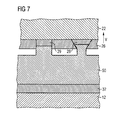
- the material 50 is selected so that the embossed structure is substantially retained even when the pressure applied by the module contact device 26 decreases. This is in Fig. 7 shown as an example.
- FIG. 12 illustrates a vertical displacement of the module 20 (in the direction of arrow V) relative to the data carrier body 12 with the component contactor 32 and the resilient, electrically conductive material 50. If the pressure on the material 50 diminishes as the contact surface of the module contactor 26 recedes, so The material 50 relaxes to a limited extent to its initial thickness (see. Fig. 5 ). For this reason, the contact between the module contact device 26 and the material 50 at a slight Displacement of the module 20 is maintained.
Landscapes
- Engineering & Computer Science (AREA)
- Microelectronics & Electronic Packaging (AREA)
- Computer Hardware Design (AREA)
- Physics & Mathematics (AREA)
- General Physics & Mathematics (AREA)
- Theoretical Computer Science (AREA)
- Metallurgy (AREA)
- Manufacturing & Machinery (AREA)
- Credit Cards Or The Like (AREA)
- Structures For Mounting Electric Components On Printed Circuit Boards (AREA)
- Coupling Device And Connection With Printed Circuit (AREA)
Priority Applications (1)
| Application Number | Priority Date | Filing Date | Title |
|---|---|---|---|
| EP13000069.8A EP2595095B1 (fr) | 2009-08-14 | 2010-08-12 | Support de données portable |
Applications Claiming Priority (1)
| Application Number | Priority Date | Filing Date | Title |
|---|---|---|---|
| DE102009037627A DE102009037627A1 (de) | 2009-08-14 | 2009-08-14 | Portabler Datenträger |
Related Child Applications (2)
| Application Number | Title | Priority Date | Filing Date |
|---|---|---|---|
| EP13000069.8A Division EP2595095B1 (fr) | 2009-08-14 | 2010-08-12 | Support de données portable |
| EP13000069.8A Division-Into EP2595095B1 (fr) | 2009-08-14 | 2010-08-12 | Support de données portable |
Publications (3)
| Publication Number | Publication Date |
|---|---|
| EP2290590A2 true EP2290590A2 (fr) | 2011-03-02 |
| EP2290590A3 EP2290590A3 (fr) | 2011-07-27 |
| EP2290590B1 EP2290590B1 (fr) | 2015-03-11 |
Family
ID=43248648
Family Applications (2)
| Application Number | Title | Priority Date | Filing Date |
|---|---|---|---|
| EP13000069.8A Not-in-force EP2595095B1 (fr) | 2009-08-14 | 2010-08-12 | Support de données portable |
| EP10008397.1A Not-in-force EP2290590B1 (fr) | 2009-08-14 | 2010-08-12 | Support de données portatif |
Family Applications Before (1)
| Application Number | Title | Priority Date | Filing Date |
|---|---|---|---|
| EP13000069.8A Not-in-force EP2595095B1 (fr) | 2009-08-14 | 2010-08-12 | Support de données portable |
Country Status (2)
| Country | Link |
|---|---|
| EP (2) | EP2595095B1 (fr) |
| DE (1) | DE102009037627A1 (fr) |
Cited By (1)
| Publication number | Priority date | Publication date | Assignee | Title |
|---|---|---|---|---|
| WO2016206801A1 (fr) * | 2015-06-23 | 2016-12-29 | Pretema Gmbh | Carte intelligente vierge comprenant au moins une interface pour la transmission sans contact d'informations |
Citations (8)
| Publication number | Priority date | Publication date | Assignee | Title |
|---|---|---|---|---|
| DE10257111A1 (de) | 2002-12-05 | 2004-07-01 | Mühlbauer Ag | Chipkarte und Verfahren zur Herstellung einer Chipkarte |
| DE102004053291A1 (de) | 2004-11-04 | 2006-05-11 | Giesecke & Devrient Gmbh | Kartenförmiger Datenträger |
| DE102004053292A1 (de) | 2004-11-04 | 2006-05-11 | Giesecke & Devrient Gmbh | Kartenförmiger Datenträger |
| DE102005002726A1 (de) | 2005-01-20 | 2006-07-27 | Giesecke & Devrient Gmbh | Tragbarer Datenträger |
| DE102005002731A1 (de) | 2005-01-20 | 2006-08-03 | Giesecke & Devrient Gmbh | Tragbarer Datenträger |
| DE102005002728A1 (de) | 2005-01-20 | 2006-08-03 | Giesecke & Devrient Gmbh | Tragbarer Datenträger |
| DE102005002732A1 (de) | 2005-01-20 | 2006-08-03 | Giesecke & Devrient Gmbh | Tragbarer Datenträger |
| DE102005002733A1 (de) | 2005-01-20 | 2006-08-17 | Giesecke & Devrient Gmbh | Tragbarer Datenträger |
Family Cites Families (11)
| Publication number | Priority date | Publication date | Assignee | Title |
|---|---|---|---|---|
| FR2703806B1 (fr) * | 1993-04-06 | 1995-07-13 | Leroux Gilles Sa | Objet portatif et procede de fabrication. |
| DE4440721A1 (de) * | 1994-11-15 | 1996-05-23 | Datacolor Druck Und Fullservic | Trägerelement für IC-Baustein |
| DE19500925C2 (de) * | 1995-01-16 | 1999-04-08 | Orga Kartensysteme Gmbh | Verfahren zur Herstellung einer kontaktlosen Chipkarte |
| US5971253A (en) * | 1995-07-31 | 1999-10-26 | Tessera, Inc. | Microelectronic component mounting with deformable shell terminals |
| WO2000036557A1 (fr) * | 1998-12-11 | 2000-06-22 | Slunsky Lubomir | Carte a puce comprenant un module a cadre de conducteurs mis en forme et procede de fabrication |
| DE19905886A1 (de) * | 1999-02-11 | 2000-08-17 | Meto International Gmbh | Identifizierungselement und Verfahren zur Herstellung eines Identifizierungselements |
| US6451875B1 (en) * | 1999-10-12 | 2002-09-17 | Sony Chemicals Corporation | Connecting material for anisotropically electroconductive connection |
| FR2826153B1 (fr) * | 2001-06-14 | 2004-05-28 | A S K | Procede de connexion d'une puce a une antenne d'un dispositif d'identification par radio-frequence du type carte a puce sans contact |
| DE102004010715B4 (de) * | 2004-03-04 | 2009-10-01 | Infineon Technologies Ag | Chipkarte zur kontaktlosen Datenübertragung sowie Verfahren zum Herstellen einer Chipkarte zur kontaktlosen Datenübertragung |
| DE102004029589A1 (de) * | 2004-06-18 | 2005-12-29 | Tesa Ag | Elektrisch anisotrop leitfähiger Schmelzkleber zur Implantierung von elektrischen Modulen in einen Kartenkörper |
| WO2009026998A2 (fr) * | 2007-08-27 | 2009-03-05 | Att Technology Gmbh | Connexion d'une puce pourvue de surfaces de connexion et de bosses à un substrat pourvu de pistes conductrices métalliques |
-
2009
- 2009-08-14 DE DE102009037627A patent/DE102009037627A1/de not_active Withdrawn
-
2010
- 2010-08-12 EP EP13000069.8A patent/EP2595095B1/fr not_active Not-in-force
- 2010-08-12 EP EP10008397.1A patent/EP2290590B1/fr not_active Not-in-force
Patent Citations (8)
| Publication number | Priority date | Publication date | Assignee | Title |
|---|---|---|---|---|
| DE10257111A1 (de) | 2002-12-05 | 2004-07-01 | Mühlbauer Ag | Chipkarte und Verfahren zur Herstellung einer Chipkarte |
| DE102004053291A1 (de) | 2004-11-04 | 2006-05-11 | Giesecke & Devrient Gmbh | Kartenförmiger Datenträger |
| DE102004053292A1 (de) | 2004-11-04 | 2006-05-11 | Giesecke & Devrient Gmbh | Kartenförmiger Datenträger |
| DE102005002726A1 (de) | 2005-01-20 | 2006-07-27 | Giesecke & Devrient Gmbh | Tragbarer Datenträger |
| DE102005002731A1 (de) | 2005-01-20 | 2006-08-03 | Giesecke & Devrient Gmbh | Tragbarer Datenträger |
| DE102005002728A1 (de) | 2005-01-20 | 2006-08-03 | Giesecke & Devrient Gmbh | Tragbarer Datenträger |
| DE102005002732A1 (de) | 2005-01-20 | 2006-08-03 | Giesecke & Devrient Gmbh | Tragbarer Datenträger |
| DE102005002733A1 (de) | 2005-01-20 | 2006-08-17 | Giesecke & Devrient Gmbh | Tragbarer Datenträger |
Cited By (3)
| Publication number | Priority date | Publication date | Assignee | Title |
|---|---|---|---|---|
| WO2016206801A1 (fr) * | 2015-06-23 | 2016-12-29 | Pretema Gmbh | Carte intelligente vierge comprenant au moins une interface pour la transmission sans contact d'informations |
| KR20180019666A (ko) * | 2015-06-23 | 2018-02-26 | 랑셍 홀딩 | 정보의 무접촉 전송을 위한 적어도 하나의 인터페이스를 가진 스마트 카드 블랭크 |
| KR102251694B1 (ko) | 2015-06-23 | 2021-05-13 | 랑셍 홀딩 | 정보의 무접촉 전송을 위한 적어도 하나의 인터페이스를 가진 스마트 카드 블랭크 |
Also Published As
| Publication number | Publication date |
|---|---|
| EP2290590A3 (fr) | 2011-07-27 |
| EP2595095B1 (fr) | 2016-07-13 |
| DE102009037627A1 (de) | 2011-02-17 |
| EP2595095A1 (fr) | 2013-05-22 |
| EP2290590B1 (fr) | 2015-03-11 |
Similar Documents
| Publication | Publication Date | Title |
|---|---|---|
| DE102004011702B4 (de) | Verfahren zur Herstellung eines Kartenkörpers für eine kontaktlose Chipkarte | |
| DE10257111B4 (de) | Chipkarte und Verfahren zur Herstellung einer Chipkarte | |
| WO1999005647A1 (fr) | Support de donnees exploitable sans contact | |
| DE3111516C2 (fr) | ||
| EP2637129B1 (fr) | Procédé de mise à nu d'un dispositif de mise en contact d'un composant électrique dans un support de données portable | |
| EP2290590B1 (fr) | Support de données portatif | |
| DE10108080C1 (de) | Kontaktlos arbeitender Datenträger mit einer kapazitiv an das Modul gekoppelten Antennenspule | |
| DE102007022615A1 (de) | Kontaktloses Übertragungssystem und Verfahren zum Herstellen desselben | |
| WO2014016411A1 (fr) | Module électronique comprenant une protection contre les manipulations | |
| EP2817768B1 (fr) | Module électronique et support de données portatif équipé dudit module électronique et leur procédé de production | |
| EP1779304B1 (fr) | Procede de production d'un support de donnees portatif | |
| EP3317821B1 (fr) | Carte intelligente vierge comprenant au moins une interface pour la transmission sans contact d'informations | |
| EP1610261B1 (fr) | Module pour carte à puce | |
| EP2817767B1 (fr) | Module électronique et support de données portatif équipé dudit module électronique et leur procédé de production | |
| DE19612718B4 (de) | Chipkarte mit Batterie sowie Verfahren zur Montage einer Chipmodul/Batterie-Einheit | |
| DE102004053292A1 (de) | Kartenförmiger Datenträger | |
| DE102005002728A1 (de) | Tragbarer Datenträger | |
| DE102005054418B4 (de) | Verfahren zum Herstellen einer Kontaktzone für eine Chipkarte | |
| DE102005002733B4 (de) | Tragbarer Datenträger | |
| DE102005002732A1 (de) | Tragbarer Datenträger | |
| DE102005002731A1 (de) | Tragbarer Datenträger | |
| DE102005002726A1 (de) | Tragbarer Datenträger | |
| DE102004053291A1 (de) | Kartenförmiger Datenträger | |
| DE202015004427U1 (de) | Smartcard-Rohling mit mindestens einer Schnittstelle zur berührungslosen Übertragung von Informationen | |
| DE102015007970A1 (de) | Smartcard-Rohling mit mindestens einer Schnittstelle zur berührungslosen Übertragung von Informationen |
Legal Events
| Date | Code | Title | Description |
|---|---|---|---|
| PUAI | Public reference made under article 153(3) epc to a published international application that has entered the european phase |
Free format text: ORIGINAL CODE: 0009012 |
|
| AK | Designated contracting states |
Kind code of ref document: A2 Designated state(s): AL AT BE BG CH CY CZ DE DK EE ES FI FR GB GR HR HU IE IS IT LI LT LU LV MC MK MT NL NO PL PT RO SE SI SK SM TR |
|
| AX | Request for extension of the european patent |
Extension state: BA ME RS |
|
| PUAL | Search report despatched |
Free format text: ORIGINAL CODE: 0009013 |
|
| AK | Designated contracting states |
Kind code of ref document: A3 Designated state(s): AL AT BE BG CH CY CZ DE DK EE ES FI FR GB GR HR HU IE IS IT LI LT LU LV MC MK MT NL NO PL PT RO SE SI SK SM TR |
|
| AX | Request for extension of the european patent |
Extension state: BA ME RS |
|
| 17P | Request for examination filed |
Effective date: 20120127 |
|
| 17Q | First examination report despatched |
Effective date: 20130311 |
|
| GRAP | Despatch of communication of intention to grant a patent |
Free format text: ORIGINAL CODE: EPIDOSNIGR1 |
|
| RIC1 | Information provided on ipc code assigned before grant |
Ipc: H05K 1/18 20060101ALI20141001BHEP Ipc: G06K 19/077 20060101AFI20141001BHEP Ipc: H01L 23/52 20060101ALI20141001BHEP Ipc: H05K 3/32 20060101ALI20141001BHEP Ipc: H05K 3/40 20060101ALI20141001BHEP Ipc: H05K 3/30 20060101ALI20141001BHEP Ipc: H01L 23/13 20060101ALI20141001BHEP Ipc: H01L 23/498 20060101ALI20141001BHEP |
|
| INTG | Intention to grant announced |
Effective date: 20141016 |
|
| GRAS | Grant fee paid |
Free format text: ORIGINAL CODE: EPIDOSNIGR3 |
|
| GRAA | (expected) grant |
Free format text: ORIGINAL CODE: 0009210 |
|
| AK | Designated contracting states |
Kind code of ref document: B1 Designated state(s): AL AT BE BG CH CY CZ DE DK EE ES FI FR GB GR HR HU IE IS IT LI LT LU LV MC MK MT NL NO PL PT RO SE SI SK SM TR |
|
| REG | Reference to a national code |
Ref country code: GB Ref legal event code: FG4D Free format text: NOT ENGLISH |
|
| REG | Reference to a national code |
Ref country code: CH Ref legal event code: EP |
|
| REG | Reference to a national code |
Ref country code: IE Ref legal event code: FG4D Free format text: LANGUAGE OF EP DOCUMENT: GERMAN |
|
| REG | Reference to a national code |
Ref country code: AT Ref legal event code: REF Ref document number: 715684 Country of ref document: AT Kind code of ref document: T Effective date: 20150415 |
|
| REG | Reference to a national code |
Ref country code: DE Ref legal event code: R096 Ref document number: 502010009095 Country of ref document: DE Effective date: 20150423 |
|
| REG | Reference to a national code |
Ref country code: NL Ref legal event code: VDEP Effective date: 20150311 |
|
| REG | Reference to a national code |
Ref country code: NL Ref legal event code: VDEP Effective date: 20150311 |
|
| PG25 | Lapsed in a contracting state [announced via postgrant information from national office to epo] |
Ref country code: HR Free format text: LAPSE BECAUSE OF FAILURE TO SUBMIT A TRANSLATION OF THE DESCRIPTION OR TO PAY THE FEE WITHIN THE PRESCRIBED TIME-LIMIT Effective date: 20150311 Ref country code: NO Free format text: LAPSE BECAUSE OF FAILURE TO SUBMIT A TRANSLATION OF THE DESCRIPTION OR TO PAY THE FEE WITHIN THE PRESCRIBED TIME-LIMIT Effective date: 20150611 Ref country code: ES Free format text: LAPSE BECAUSE OF FAILURE TO SUBMIT A TRANSLATION OF THE DESCRIPTION OR TO PAY THE FEE WITHIN THE PRESCRIBED TIME-LIMIT Effective date: 20150311 Ref country code: FI Free format text: LAPSE BECAUSE OF FAILURE TO SUBMIT A TRANSLATION OF THE DESCRIPTION OR TO PAY THE FEE WITHIN THE PRESCRIBED TIME-LIMIT Effective date: 20150311 Ref country code: LT Free format text: LAPSE BECAUSE OF FAILURE TO SUBMIT A TRANSLATION OF THE DESCRIPTION OR TO PAY THE FEE WITHIN THE PRESCRIBED TIME-LIMIT Effective date: 20150311 Ref country code: SE Free format text: LAPSE BECAUSE OF FAILURE TO SUBMIT A TRANSLATION OF THE DESCRIPTION OR TO PAY THE FEE WITHIN THE PRESCRIBED TIME-LIMIT Effective date: 20150311 |
|
| REG | Reference to a national code |
Ref country code: FR Ref legal event code: PLFP Year of fee payment: 6 |
|
| REG | Reference to a national code |
Ref country code: LT Ref legal event code: MG4D |
|
| PG25 | Lapsed in a contracting state [announced via postgrant information from national office to epo] |
Ref country code: GR Free format text: LAPSE BECAUSE OF FAILURE TO SUBMIT A TRANSLATION OF THE DESCRIPTION OR TO PAY THE FEE WITHIN THE PRESCRIBED TIME-LIMIT Effective date: 20150612 Ref country code: LV Free format text: LAPSE BECAUSE OF FAILURE TO SUBMIT A TRANSLATION OF THE DESCRIPTION OR TO PAY THE FEE WITHIN THE PRESCRIBED TIME-LIMIT Effective date: 20150311 |
|
| PG25 | Lapsed in a contracting state [announced via postgrant information from national office to epo] |
Ref country code: NL Free format text: LAPSE BECAUSE OF FAILURE TO SUBMIT A TRANSLATION OF THE DESCRIPTION OR TO PAY THE FEE WITHIN THE PRESCRIBED TIME-LIMIT Effective date: 20150311 |
|
| PG25 | Lapsed in a contracting state [announced via postgrant information from national office to epo] |
Ref country code: EE Free format text: LAPSE BECAUSE OF FAILURE TO SUBMIT A TRANSLATION OF THE DESCRIPTION OR TO PAY THE FEE WITHIN THE PRESCRIBED TIME-LIMIT Effective date: 20150311 Ref country code: RO Free format text: LAPSE BECAUSE OF FAILURE TO SUBMIT A TRANSLATION OF THE DESCRIPTION OR TO PAY THE FEE WITHIN THE PRESCRIBED TIME-LIMIT Effective date: 20150311 Ref country code: SK Free format text: LAPSE BECAUSE OF FAILURE TO SUBMIT A TRANSLATION OF THE DESCRIPTION OR TO PAY THE FEE WITHIN THE PRESCRIBED TIME-LIMIT Effective date: 20150311 Ref country code: PT Free format text: LAPSE BECAUSE OF FAILURE TO SUBMIT A TRANSLATION OF THE DESCRIPTION OR TO PAY THE FEE WITHIN THE PRESCRIBED TIME-LIMIT Effective date: 20150713 Ref country code: CZ Free format text: LAPSE BECAUSE OF FAILURE TO SUBMIT A TRANSLATION OF THE DESCRIPTION OR TO PAY THE FEE WITHIN THE PRESCRIBED TIME-LIMIT Effective date: 20150311 |
|
| PG25 | Lapsed in a contracting state [announced via postgrant information from national office to epo] |
Ref country code: PL Free format text: LAPSE BECAUSE OF FAILURE TO SUBMIT A TRANSLATION OF THE DESCRIPTION OR TO PAY THE FEE WITHIN THE PRESCRIBED TIME-LIMIT Effective date: 20150311 Ref country code: IS Free format text: LAPSE BECAUSE OF FAILURE TO SUBMIT A TRANSLATION OF THE DESCRIPTION OR TO PAY THE FEE WITHIN THE PRESCRIBED TIME-LIMIT Effective date: 20150711 |
|
| REG | Reference to a national code |
Ref country code: DE Ref legal event code: R097 Ref document number: 502010009095 Country of ref document: DE |
|
| PG25 | Lapsed in a contracting state [announced via postgrant information from national office to epo] |
Ref country code: IT Free format text: LAPSE BECAUSE OF FAILURE TO SUBMIT A TRANSLATION OF THE DESCRIPTION OR TO PAY THE FEE WITHIN THE PRESCRIBED TIME-LIMIT Effective date: 20150311 |
|
| PLBE | No opposition filed within time limit |
Free format text: ORIGINAL CODE: 0009261 |
|
| STAA | Information on the status of an ep patent application or granted ep patent |
Free format text: STATUS: NO OPPOSITION FILED WITHIN TIME LIMIT |
|
| PG25 | Lapsed in a contracting state [announced via postgrant information from national office to epo] |
Ref country code: DK Free format text: LAPSE BECAUSE OF FAILURE TO SUBMIT A TRANSLATION OF THE DESCRIPTION OR TO PAY THE FEE WITHIN THE PRESCRIBED TIME-LIMIT Effective date: 20150311 |
|
| 26N | No opposition filed |
Effective date: 20151214 |
|
| PG25 | Lapsed in a contracting state [announced via postgrant information from national office to epo] |
Ref country code: SI Free format text: LAPSE BECAUSE OF FAILURE TO SUBMIT A TRANSLATION OF THE DESCRIPTION OR TO PAY THE FEE WITHIN THE PRESCRIBED TIME-LIMIT Effective date: 20150311 |
|
| PG25 | Lapsed in a contracting state [announced via postgrant information from national office to epo] |
Ref country code: MC Free format text: LAPSE BECAUSE OF FAILURE TO SUBMIT A TRANSLATION OF THE DESCRIPTION OR TO PAY THE FEE WITHIN THE PRESCRIBED TIME-LIMIT Effective date: 20150311 Ref country code: LU Free format text: LAPSE BECAUSE OF FAILURE TO SUBMIT A TRANSLATION OF THE DESCRIPTION OR TO PAY THE FEE WITHIN THE PRESCRIBED TIME-LIMIT Effective date: 20150812 |
|
| REG | Reference to a national code |
Ref country code: CH Ref legal event code: PL |
|
| GBPC | Gb: european patent ceased through non-payment of renewal fee |
Effective date: 20150812 |
|
| PG25 | Lapsed in a contracting state [announced via postgrant information from national office to epo] |
Ref country code: CH Free format text: LAPSE BECAUSE OF NON-PAYMENT OF DUE FEES Effective date: 20150831 Ref country code: LI Free format text: LAPSE BECAUSE OF NON-PAYMENT OF DUE FEES Effective date: 20150831 |
|
| REG | Reference to a national code |
Ref country code: IE Ref legal event code: MM4A |
|
| PG25 | Lapsed in a contracting state [announced via postgrant information from national office to epo] |
Ref country code: GB Free format text: LAPSE BECAUSE OF NON-PAYMENT OF DUE FEES Effective date: 20150812 Ref country code: IE Free format text: LAPSE BECAUSE OF NON-PAYMENT OF DUE FEES Effective date: 20150812 |
|
| REG | Reference to a national code |
Ref country code: FR Ref legal event code: PLFP Year of fee payment: 7 |
|
| REG | Reference to a national code |
Ref country code: AT Ref legal event code: MM01 Ref document number: 715684 Country of ref document: AT Kind code of ref document: T Effective date: 20150812 |
|
| PG25 | Lapsed in a contracting state [announced via postgrant information from national office to epo] |
Ref country code: AT Free format text: LAPSE BECAUSE OF NON-PAYMENT OF DUE FEES Effective date: 20150812 |
|
| PG25 | Lapsed in a contracting state [announced via postgrant information from national office to epo] |
Ref country code: MT Free format text: LAPSE BECAUSE OF FAILURE TO SUBMIT A TRANSLATION OF THE DESCRIPTION OR TO PAY THE FEE WITHIN THE PRESCRIBED TIME-LIMIT Effective date: 20150311 |
|
| PG25 | Lapsed in a contracting state [announced via postgrant information from national office to epo] |
Ref country code: HU Free format text: LAPSE BECAUSE OF FAILURE TO SUBMIT A TRANSLATION OF THE DESCRIPTION OR TO PAY THE FEE WITHIN THE PRESCRIBED TIME-LIMIT; INVALID AB INITIO Effective date: 20100812 Ref country code: BG Free format text: LAPSE BECAUSE OF FAILURE TO SUBMIT A TRANSLATION OF THE DESCRIPTION OR TO PAY THE FEE WITHIN THE PRESCRIBED TIME-LIMIT Effective date: 20150311 Ref country code: SM Free format text: LAPSE BECAUSE OF FAILURE TO SUBMIT A TRANSLATION OF THE DESCRIPTION OR TO PAY THE FEE WITHIN THE PRESCRIBED TIME-LIMIT Effective date: 20150311 |
|
| PG25 | Lapsed in a contracting state [announced via postgrant information from national office to epo] |
Ref country code: CY Free format text: LAPSE BECAUSE OF FAILURE TO SUBMIT A TRANSLATION OF THE DESCRIPTION OR TO PAY THE FEE WITHIN THE PRESCRIBED TIME-LIMIT Effective date: 20150311 |
|
| REG | Reference to a national code |
Ref country code: DE Ref legal event code: R081 Ref document number: 502010009095 Country of ref document: DE Owner name: GIESECKE+DEVRIENT MOBILE SECURITY GMBH, DE Free format text: FORMER OWNER: GIESECKE DEVRIENT GMBH, 81677 MUENCHEN, DE Ref country code: DE Ref legal event code: R081 Ref document number: 502010009095 Country of ref document: DE Owner name: GIESECKE+DEVRIENT MOBILE SECURITY GMBH, DE Free format text: FORMER OWNER: GIESECKE & DEVRIENT GMBH, 81677 MUENCHEN, DE |
|
| PG25 | Lapsed in a contracting state [announced via postgrant information from national office to epo] |
Ref country code: BE Free format text: LAPSE BECAUSE OF NON-PAYMENT OF DUE FEES Effective date: 20150831 |
|
| REG | Reference to a national code |
Ref country code: FR Ref legal event code: PLFP Year of fee payment: 8 |
|
| PG25 | Lapsed in a contracting state [announced via postgrant information from national office to epo] |
Ref country code: TR Free format text: LAPSE BECAUSE OF FAILURE TO SUBMIT A TRANSLATION OF THE DESCRIPTION OR TO PAY THE FEE WITHIN THE PRESCRIBED TIME-LIMIT Effective date: 20150311 |
|
| PG25 | Lapsed in a contracting state [announced via postgrant information from national office to epo] |
Ref country code: MK Free format text: LAPSE BECAUSE OF FAILURE TO SUBMIT A TRANSLATION OF THE DESCRIPTION OR TO PAY THE FEE WITHIN THE PRESCRIBED TIME-LIMIT Effective date: 20150311 |
|
| REG | Reference to a national code |
Ref country code: FR Ref legal event code: TP Owner name: GIESECKE+DEVRIENT MOBILE SECURITY GMBH, DE Effective date: 20180619 |
|
| REG | Reference to a national code |
Ref country code: FR Ref legal event code: PLFP Year of fee payment: 9 |
|
| PG25 | Lapsed in a contracting state [announced via postgrant information from national office to epo] |
Ref country code: AL Free format text: LAPSE BECAUSE OF FAILURE TO SUBMIT A TRANSLATION OF THE DESCRIPTION OR TO PAY THE FEE WITHIN THE PRESCRIBED TIME-LIMIT Effective date: 20150311 |
|
| P01 | Opt-out of the competence of the unified patent court (upc) registered |
Effective date: 20230520 |
|
| REG | Reference to a national code |
Ref country code: DE Ref legal event code: R081 Ref document number: 502010009095 Country of ref document: DE Owner name: GIESECKE+DEVRIENT EPAYMENTS GMBH, DE Free format text: FORMER OWNER: GIESECKE+DEVRIENT MOBILE SECURITY GMBH, 81677 MUENCHEN, DE |
|
| PGFP | Annual fee paid to national office [announced via postgrant information from national office to epo] |
Ref country code: FR Payment date: 20230821 Year of fee payment: 14 Ref country code: DE Payment date: 20230831 Year of fee payment: 14 |
|
| REG | Reference to a national code |
Ref country code: DE Ref legal event code: R119 Ref document number: 502010009095 Country of ref document: DE |
|
| PG25 | Lapsed in a contracting state [announced via postgrant information from national office to epo] |
Ref country code: DE Free format text: LAPSE BECAUSE OF NON-PAYMENT OF DUE FEES Effective date: 20250301 |
|
| PG25 | Lapsed in a contracting state [announced via postgrant information from national office to epo] |
Ref country code: FR Free format text: LAPSE BECAUSE OF NON-PAYMENT OF DUE FEES Effective date: 20240831 |