EP2290692A1 - Élément d analyse d image à l état solide - Google Patents
Élément d analyse d image à l état solide Download PDFInfo
- Publication number
- EP2290692A1 EP2290692A1 EP09738894A EP09738894A EP2290692A1 EP 2290692 A1 EP2290692 A1 EP 2290692A1 EP 09738894 A EP09738894 A EP 09738894A EP 09738894 A EP09738894 A EP 09738894A EP 2290692 A1 EP2290692 A1 EP 2290692A1
- Authority
- EP
- European Patent Office
- Prior art keywords
- solid
- state imaging
- diffusion layer
- type diffusion
- island
- Prior art date
- Legal status (The legal status is an assumption and is not a legal conclusion. Google has not performed a legal analysis and makes no representation as to the accuracy of the status listed.)
- Withdrawn
Links
Images


Classifications
-
- H—ELECTRICITY
- H10—SEMICONDUCTOR DEVICES; ELECTRIC SOLID-STATE DEVICES NOT OTHERWISE PROVIDED FOR
- H10F—INORGANIC SEMICONDUCTOR DEVICES SENSITIVE TO INFRARED RADIATION, LIGHT, ELECTROMAGNETIC RADIATION OF SHORTER WAVELENGTH OR CORPUSCULAR RADIATION
- H10F39/00—Integrated devices, or assemblies of multiple devices, comprising at least one element covered by group H10F30/00, e.g. radiation detectors comprising photodiode arrays
- H10F39/80—Constructional details of image sensors
- H10F39/802—Geometry or disposition of elements in pixels, e.g. address-lines or gate electrodes
- H10F39/8027—Geometry of the photosensitive area
-
- H—ELECTRICITY
- H10—SEMICONDUCTOR DEVICES; ELECTRIC SOLID-STATE DEVICES NOT OTHERWISE PROVIDED FOR
- H10F—INORGANIC SEMICONDUCTOR DEVICES SENSITIVE TO INFRARED RADIATION, LIGHT, ELECTROMAGNETIC RADIATION OF SHORTER WAVELENGTH OR CORPUSCULAR RADIATION
- H10F39/00—Integrated devices, or assemblies of multiple devices, comprising at least one element covered by group H10F30/00, e.g. radiation detectors comprising photodiode arrays
- H10F39/80—Constructional details of image sensors
- H10F39/803—Pixels having integrated switching, control, storage or amplification elements
- H10F39/8033—Photosensitive area
-
- H—ELECTRICITY
- H10—SEMICONDUCTOR DEVICES; ELECTRIC SOLID-STATE DEVICES NOT OTHERWISE PROVIDED FOR
- H10F—INORGANIC SEMICONDUCTOR DEVICES SENSITIVE TO INFRARED RADIATION, LIGHT, ELECTROMAGNETIC RADIATION OF SHORTER WAVELENGTH OR CORPUSCULAR RADIATION
- H10F39/00—Integrated devices, or assemblies of multiple devices, comprising at least one element covered by group H10F30/00, e.g. radiation detectors comprising photodiode arrays
- H10F39/80—Constructional details of image sensors
- H10F39/803—Pixels having integrated switching, control, storage or amplification elements
- H10F39/8037—Pixels having integrated switching, control, storage or amplification elements the integrated elements comprising a transistor
- H10F39/80373—Pixels having integrated switching, control, storage or amplification elements the integrated elements comprising a transistor characterised by the gate of the transistor
-
- H—ELECTRICITY
- H10—SEMICONDUCTOR DEVICES; ELECTRIC SOLID-STATE DEVICES NOT OTHERWISE PROVIDED FOR
- H10D—INORGANIC ELECTRIC SEMICONDUCTOR DEVICES
- H10D64/00—Electrodes of devices having potential barriers
- H10D64/20—Electrodes characterised by their shapes, relative sizes or dispositions
- H10D64/27—Electrodes not carrying the current to be rectified, amplified, oscillated or switched, e.g. gates
- H10D64/311—Gate electrodes for field-effect devices
- H10D64/411—Gate electrodes for field-effect devices for FETs
- H10D64/511—Gate electrodes for field-effect devices for FETs for IGFETs
- H10D64/512—Disposition of the gate electrodes, e.g. buried gates
-
- H—ELECTRICITY
- H10—SEMICONDUCTOR DEVICES; ELECTRIC SOLID-STATE DEVICES NOT OTHERWISE PROVIDED FOR
- H10D—INORGANIC ELECTRIC SEMICONDUCTOR DEVICES
- H10D64/00—Electrodes of devices having potential barriers
- H10D64/20—Electrodes characterised by their shapes, relative sizes or dispositions
- H10D64/27—Electrodes not carrying the current to be rectified, amplified, oscillated or switched, e.g. gates
- H10D64/311—Gate electrodes for field-effect devices
- H10D64/411—Gate electrodes for field-effect devices for FETs
- H10D64/511—Gate electrodes for field-effect devices for FETs for IGFETs
- H10D64/517—Gate electrodes for field-effect devices for FETs for IGFETs characterised by the conducting layers
- H10D64/518—Gate electrodes for field-effect devices for FETs for IGFETs characterised by the conducting layers characterised by their lengths or sectional shapes
-
- H—ELECTRICITY
- H10—SEMICONDUCTOR DEVICES; ELECTRIC SOLID-STATE DEVICES NOT OTHERWISE PROVIDED FOR
- H10D—INORGANIC ELECTRIC SEMICONDUCTOR DEVICES
- H10D64/00—Electrodes of devices having potential barriers
- H10D64/20—Electrodes characterised by their shapes, relative sizes or dispositions
- H10D64/27—Electrodes not carrying the current to be rectified, amplified, oscillated or switched, e.g. gates
- H10D64/311—Gate electrodes for field-effect devices
- H10D64/411—Gate electrodes for field-effect devices for FETs
- H10D64/511—Gate electrodes for field-effect devices for FETs for IGFETs
- H10D64/517—Gate electrodes for field-effect devices for FETs for IGFETs characterised by the conducting layers
- H10D64/519—Gate electrodes for field-effect devices for FETs for IGFETs characterised by the conducting layers characterised by their top-view geometrical layouts
-
- H—ELECTRICITY
- H10—SEMICONDUCTOR DEVICES; ELECTRIC SOLID-STATE DEVICES NOT OTHERWISE PROVIDED FOR
- H10F—INORGANIC SEMICONDUCTOR DEVICES SENSITIVE TO INFRARED RADIATION, LIGHT, ELECTROMAGNETIC RADIATION OF SHORTER WAVELENGTH OR CORPUSCULAR RADIATION
- H10F39/00—Integrated devices, or assemblies of multiple devices, comprising at least one element covered by group H10F30/00, e.g. radiation detectors comprising photodiode arrays
- H10F39/10—Integrated devices
- H10F39/12—Image sensors
- H10F39/196—Junction field effect transistor [JFET] image sensors; Static induction transistor [SIT] image sensors
-
- H—ELECTRICITY
- H10—SEMICONDUCTOR DEVICES; ELECTRIC SOLID-STATE DEVICES NOT OTHERWISE PROVIDED FOR
- H10P—GENERIC PROCESSES OR APPARATUS FOR THE MANUFACTURE OR TREATMENT OF DEVICES COVERED BY CLASS H10
- H10P50/00—Etching of wafers, substrates or parts of devices
- H10P50/69—Etching of wafers, substrates or parts of devices using masks for semiconductor materials
- H10P50/691—Etching of wafers, substrates or parts of devices using masks for semiconductor materials for Group V materials or Group III-V materials
- H10P50/693—Etching of wafers, substrates or parts of devices using masks for semiconductor materials for Group V materials or Group III-V materials characterised by their size, orientation, disposition, behaviour or shape, in horizontal or vertical plane
Definitions
- the present invention relates to a solid-state imaging device.
- CMOS image sensor a photoelectric conversion section, an amplification section, a pixel selection section and a reset section are formed in one pixel, wherein three MOS transistors are used for the sections other than the photoelectric conversion section composed of a photodiode (see, for example, the Patent Publication 1).
- the conventional CMOS image sensor consists of four elements.
- the CMOS image sensor is operable to store electric charges generated by the photoelectric conversion section composed of a photodiode, and, after amplifying the stored electric charges through the amplification section, read the amplified electric charges using the pixel selection section.
- FIG. 1 shows a unit pixel of the conventional CMOS image sensor.
- the reference numeral 001 indicates a photoelectric-conversion photodiode.
- the reference numerals 006, 007 and 008 indicate an amplification transistor, a reset transistor and a selection transistor, respectively.
- the reference numerals 004, 002, 003, 005 and 009 indicate a signal line, a pixel-selection clock line, a reset clock line, a power supply line, and a reset power supply line, respectively.
- the unit pixel of the conventional CMOS image sensor has the photodiode and the three MOS transistors in a plane. Thus, it is difficult to increase a ratio of a surface area of a light-receiving section (photodiode) to an overall surface area of one pixel.
- Non-Patent Document 1 It is reported that, in a conventional CMOS image sensor using a 0.35 ⁇ m, single polysilicon layer/double metal layer CMOS process, a ratio of a surface area of a light-receiving section (photodiode) to an overall surface area of one pixel is 17% (see the following Non-Patent Document 1). It is also reported that, in a conventional CMOS image sensor using a 0.15 ⁇ m wiring-rule process, a ratio of a surface area of a light-receiving section (photodiode) to an overall surface area of one pixel is 30% (see the following Non-Patent Document 2).
- CMOS image sensor where the ratio of the surface area of the light-receiving section (photodiode) to the overall surface area of one pixel is 30%, a microlens is formed to condense light. This means that a CMOS image sensor having a small ratio of a surface area of a light-receiving section (photodiode) to an overall surface area of one pixel requires a light-condensing microlens.
- a solid-state imaging device which comprises a signal line formed on a substrate, an island-shaped semiconductor arranged on the signal line, and a pixel selection line connected to a top of the island-shaped semiconductor.
- the island-shaped semiconductor includes: a first semiconductor layer formed as a bottom portion of the island-shaped semiconductor and connected to the signal line; a second semiconductor layer formed above and adjacent to the first semiconductor layer; a gate connected to the second semiconductor layer through a dielectric film; a charge storage section comprised of a third semiconductor layer connected to the second semiconductor layer and adapted, in response to receiving light, to undergo a change in amount of electric charges therein; and a fourth semiconductor layer formed above and adjacent to the second and third semiconductor layers.
- the pixel selection line is comprised of a transparent conductive film, and a part of the gate is disposed inside a depression formed in a sidewall of the second semiconductor layer.
- the signal line is an n+-type diffusion layer.
- the first semiconductor layer is an n+-type diffusion layer, and the second semiconductor layer is a p-type impurity-doped region.
- the third semiconductor layer is an n-type diffusion layer, and the fourth semiconductor layer is a p+-type diffusion layer.
- a combination of the p+-type diffusion layer and the n-type diffusion layer functions as a photoelectric-conversion photodiode
- a combination of the p+-type diffusion layer, the n-type diffusion layer and the p-type impurity-doped region functions as an amplification transistor.
- a combination of the n+-type diffusion layer serving as the first semiconductor layer, the p-type impurity-doped region, the n-type diffusion layer and the gate functions as a reset transistor
- a combination of the p-type impurity-doped region and the n+-type diffusion layer serving as the first semiconductor layer functions as a diode.
- the island-shaped semiconductor may have a square or rectangular pillar shape.
- the island-shaped semiconductor may have a hexagonal pillar shape.
- the island-shaped semiconductor may have a circular pillar shape.
- a solid-state imaging apparatus which comprises a plurality of the solid-state imaging devices according to the first aspect of the present invention, wherein the solid-state imaging devices are arranged in an n-row by m-column array (wherein each of n and m is an integer of 1 or more) with respect to the substrate.
- a solid-state imaging apparatus which comprises a plurality of the solid-state imaging devices each including the island-shaped semiconductor having a square or rectangular pillar shape, wherein the solid-state imaging devices are arranged in an n-row by m-column array (wherein each of n and m is an integer of 1 or more) with respect to the substrate.
- a solid-state imaging apparatus which comprises a plurality of the solid-state imaging devices each including the island-shaped semiconductor having a circular pillar shape, wherein the solid-state imaging devices are arranged in an n-row by m-column array (wherein each of n and m is an integer of 1 or more) with respect to the substrate.
- a solid-state imaging apparatus which comprises a plurality of the solid-state imaging devices according to the first aspect of the present invention, wherein the solid-state imaging devices are arranged on the substrate in a honeycomb pattern.
- a solid-state imaging apparatus which comprises a plurality of the solid-state imaging devices each including the island-shaped semiconductor having a hexagonal pillar shape, wherein the solid-state imaging devices are arranged on the substrate in a honeycomb pattern.
- a solid-state imaging apparatus which comprises a plurality of the solid-state imaging devices each including the island-shaped semiconductor having a circular pillar shape, wherein the solid-state imaging devices are arranged on the substrate in a honeycomb pattern.
- a method of producing a solid-state imaging device comprises the steps of: forming an oxide film on a silicon substrate; forming a p-type silicon on the oxide film; forming an oxide film-based mask and a nitride film-based mask by depositing a nitride film on the p-type silicon, depositing an oxide film on the nitride film, forming a resist for a silicon pillar, etching the oxide film and the nitride film, and removing the resist; forming a depression in a sidewall of a p-type impurity-doped region by etching the p-type silicon to form a silicon pillar, depositing a nitride film, etching the nitride film in such a manner that a sidewall-shaped nitride film is left on a sidewall of the silicon pillar, and isotropically etching the p-type silicon;
- a unit pixel of a conventional CMOS image sensor has a total four elements, i.e., a photodiode and three MOS transistors, in a plane. Thus, it is difficult to increase a ratio of a surface area of a light-receiving section (photodiode) to an overall surface area of one pixel. It is reported that, in a conventional CMOS image sensor using a 0.15 ⁇ m wiring-rule process, a ratio of a surface area of a light-receiving section (photodiode) to an overall surface area of one pixel is 30%.
- the present invention provides a solid-state imaging device which comprises: a signal line formed on a substrate; an island-shaped semiconductor arranged on the signal line; and a pixel selection line connected to a top of the island-shaped semiconductor, wherein the island-shaped semiconductor includes: a first semiconductor layer formed as a bottom portion of the island-shaped semiconductor and connected to the signal line; a second semiconductor layer formed above and adjacent to the first semiconductor layer; a gate connected to the second semiconductor layer through a dielectric film; a charge storage section comprised of a third semiconductor layer connected to the second semiconductor layer and adapted, in response to receiving light, to undergo a change in amount of electric charges therein; and a fourth semiconductor layer formed above and adjacent to the second and third semiconductor layers, and wherein the pixel selection line is comprised of a transparent conductive film, and a part of the gate is disposed inside a depression formed in a sidewall of the second semiconductor layer.
- a combination of the third and fourth semiconductor layers, a combination of the second, third and fourth semiconductor layers, a combination of the first, second and third semiconductor layers, and a combination of the second and first semiconductor layers function, respectively, as the photoelectric-conversion photodiode, the amplification transistor, the reset transistor, and the diode in the aforementioned unit pixel.
- a metal for use in a conventional semiconductor production process such as aluminum or copper, reflects light. Thus, it is necessary to connect a line made of such a metal to a sidewall of the fourth semiconductor layer.
- a transparent conductive film such as indium tin oxide (ITO), zinc oxide (ZnO) or tin oxide (SnO 2 ), is used as the pixel selection line to allow the pixel selection line to be connected to a top of the fourth semiconductor layer.
- ITO indium tin oxide
- ZnO zinc oxide
- SnO 2 tin oxide
- a surface area of one pixel is a sum of an area of the photodiode, an area of the gate, and an area of a region between the devices.
- a part of the gate is disposed inside a depression formed in a sidewall of the second semiconductor layer, so that a surface area of one pixel can be reduced substantially to a sum of an area of the photodiode and an area of a region between the devices.
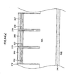
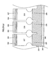
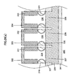
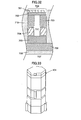
- FIG. 2 is a bird's-eye view showing a single solid-state imaging device according to a first embodiment of the present invention.
- FIG. 3 is a top plan view showing the solid-state imaging device according to the first embodiment.
- FIG. 4(a) is a sectional view taken along the line X 1 -X' 1 in FIG. 3
- FIG. 4(b) is a diagram showing an equivalent circuit of the sectional structure in FIG. 4(a)
- FIG. 5(a) is a sectional view taken along the line Y 1 -Y' 1 in FIG. 3
- FIG. 5(b) is a diagram showing an equivalent circuit of the sectional structure in FIG. 5(a) .
- an oxide film 108 is formed on a silicon substrate 107.
- a signal line 106 is formed on the oxide film 108, and an island-shaped semiconductor is formed on the signal line 106.
- the island-shaped semiconductor comprises: an n+-type diffusion layer 105 formed as a bottom portion thereof and connected to the signal line; a p-type impurity-doped region 111 formed above and adjacent to the n+-type diffusion layer; a gate 104 connected to the p-type impurity-doped region through a dielectric film; a charge storage section 103 comprised of an n-type diffusion layer connected to the p-type impurity-doped region 111 and adapted, in response to receiving light, to undergo a change in amount of electric charges therein; and a p+-type diffusion layer 102 formed above and adjacent to the p-type impurity-doped region and the n-type diffusion layer.
- a pixel selection line 101 comprised of a transparent conductive film is formed to be connected to a top of the p+-type diffusion layer 102 which is a top portion of the island-shaped semiconductor.
- the gate is formed in such a manner that a part thereof is disposed inside a depression formed in a sidewall of the p-type impurity-doped region.
- a combination of the p+-type diffusion layer 102 and the n-type diffusion layer 103 functions as a photoelectric-conversion photodiode 109.
- a combination of the p+-type diffusion layer 102, the n-type diffusion layer 103 and the p-type impurity-doped region 111 functions as an amplification transistor 113.
- a combination of the n+-type diffusion layer 105, the p-type impurity-doped region 111, the n-type diffusion layer 103 and the gate 104 functions as a reset transistor 112.
- a combination of the p-type impurity-doped region 111 and the n+-type diffusion layer 105 functions as a diode 114.
- An oxide film 110 is formed as an interlayer dielectric film.
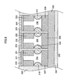
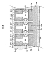
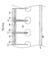
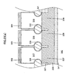
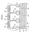
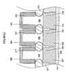
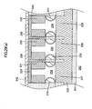
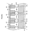
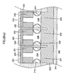
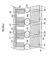
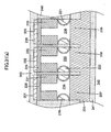
- FIG. 6 is a bird's-eye view showing a solid-state imaging device array in which a plurality of the above solid-state imaging devices are arranged in a matrix pattern.
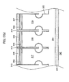
- FIG. 7 is a top plan view of the solid-state imaging device array.
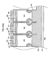
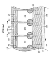
- FIG. 8 , FIG. 9 , FIG. 10 and FIG. 11 are a sectional view taken along the line X 2 -X' 2 in FIG. 7 , a sectional view taken along the line X 3 -X' 3 in FIG. 7 , a sectional view taken along the line X 4 -X' 4 in FIG. 7 and a sectional view taken along the line Y 2 -Y' 2 in FIG. 7 , respectively.
- an oxide film 241 is formed on a silicon substrate 242.
- a signal line 225 is formed on the oxide film 241, and a first island-shaped semiconductor is formed on the signal line 225.
- the first island-shaped semiconductor comprises: an n+-type diffusion layer 237 formed as a bottom portion thereof and connected to the signal line 225; a p-type impurity-doped region 234 formed above and adjacent to the n+-type diffusion layer 237; a gate 219 connected to the p-type impurity-doped region 234 through a dielectric film; a charge storage section 231 comprised of an n-type diffusion layer connected to the p-type impurity-doped region 234 and adapted, in response to receiving light, to undergo a change in amount of electric charges therein; and a p+-type diffusion layer 228 formed above and adjacent to the p-type impurity-doped region 234 and the n-type diffusion layer 231.
- a pixel selection line 201 comprised of a transparent conductive film is formed to be connected to a top of the p+-type diffusion layer 228 which is a top portion of the first island-shaped semiconductor.
- the gate 219 is formed in such a manner that a part thereof is disposed inside a depression formed in a sidewall of the p-type impurity-doped region 234.
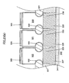
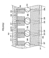
- a second island-shaped semiconductor is formed on the signal line 225 formed on the oxide film 241 formed on the silicon substrate 242.
- the second island-shaped semiconductor comprises: an n+-type diffusion layer 238 formed as a bottom portion thereof and connected to the signal line 225; a p-type impurity-doped region 235 formed above and adjacent to the n+-type diffusion layer 238; a gate 220 connected to the p-type impurity-doped region 235 through a dielectric film; a charge storage section 232 comprised of an n-type diffusion layer connected to the p-type impurity-doped region 235 and adapted, in response to receiving light, to undergo a change in amount of electric charges therein; and a p+-type diffusion layer 229 formed above and adjacent to the p-type impurity-doped region 235 and the n-type diffusion layer 232.
- a pixel selection line 202 comprised of a transparent conductive film is formed to be connected to a top of the p+-type diffusion layer 229 which is a top portion of the second island-shaped semiconductor.
- the gate 220 is formed in such a manner that a part thereof is disposed inside a depression formed in a sidewall of the p-type impurity-doped region 235.
- a third island-shaped semiconductor is formed on the signal line 225 formed on the oxide film 241 formed on the silicon substrate 242.
- the third island-shaped semiconductor comprises: an n+-type diffusion layer 239 formed as a bottom portion thereof and connected to the signal line 225; a p-type impurity-doped region 236 formed above and adjacent to the n+-type diffusion layer 239; a gate 221 connected to the p-type impurity-doped region 236 through a dielectric film; a charge storage section 233 comprised of an n-type diffusion layer connected to the p-type impurity-doped region 236 and adapted, in response to receiving light, to undergo a change in amount of electric charges therein; and a p+-type diffusion layer 230 formed above and adjacent to the p-type impurity-doped region 236 and the n-type diffusion layer 233.
- a pixel selection line 203 comprised of a transparent conductive film is formed to be connected to a top of the p+-type diffusion layer 230 which is a top portion of the third island-shaped semiconductor.
- the gate 221 is formed in such a manner that a part thereof is disposed inside a depression formed in a sidewall of the p-type impurity-doped region 236.
- An oxide film 240 is formed as an interlayer dielectric film.
- a signal line 226 is formed on the oxide film 241 formed on the silicon substrate 242, and a fourth island-shaped semiconductor is formed on the signal line 226.
- the fourth island-shaped semiconductor comprises: an n+-type diffusion layer 252 formed as a bottom portion thereof and connected to the signal line 226; a p-type impurity-doped region 249 formed above and adjacent to the n+-type diffusion layer 252; a gate 219 connected to the p-type impurity-doped region 249 through a dielectric film; a charge storage section 246 comprised of an n-type diffusion layer connected to the p-type impurity-doped region 249 and adapted, in response to receiving light, to undergo a change in amount of electric charges therein; and a p+-type diffusion layer 243 formed above and adjacent to the p-type impurity-doped region 249 and the n-type diffusion layer 246.
- the pixel selection line 201 comprised of a transparent conductive film is formed to be connected to a top of the p+-type diffusion layer 243 which is a top portion of the fourth island-shaped semiconductor.
- the gate 219 is formed in such a manner that a part thereof is disposed inside a depression formed in a sidewall of the p-type impurity-doped region 249.
- a fifth island-shaped semiconductor is formed on the signal line 226 formed on the oxide film 241 formed on the silicon substrate 242.
- the fifth island-shaped semiconductor comprises: an n+-type diffusion layer 253 formed as a bottom portion thereof and connected to the signal line 226; a p-type impurity-doped region 250 formed above and adjacent to the n+-type diffusion layer 253; a gate 220 connected to the p-type impurity-doped region 250 through a dielectric film; a charge storage section 247 comprised of an n-type diffusion layer connected to the p-type impurity-doped region 250 and adapted, in response to receiving light, to undergo a change in amount of electric charges therein; and a p+-type diffusion layer 244 formed above and adjacent to the p-type impurity-doped region 250 and the n-type diffusion layer 247.
- the pixel selection line 202 comprised of a transparent conductive film is formed to be connected to a top of the p+-type diffusion layer 244 which is a top portion of the fifth island-shaped semiconductor.
- the gate 220 is formed in such a manner that a part thereof is disposed inside a depression formed in a sidewall of the p-type impurity-doped region 250.
- a sixth island-shaped semiconductor is formed on the signal line 226 formed on the oxide film 241 formed on the silicon substrate 242.
- the sixth island-shaped semiconductor comprises: an n+-type diffusion layer 254 formed as a bottom portion thereof and connected to the signal line 226; a p-type impurity-doped region 251 formed above and adjacent to the n+-type diffusion layer 254; a gate 221 connected to the p-type impurity-doped region 251 through a dielectric film; a charge storage section 248 comprised of an n-type diffusion layer connected to the p-type impurity-doped region 251 and adapted, in response to receiving light, to undergo a change in amount of electric charges therein; and a p+-type diffusion layer 245 formed above and adjacent to the p-type impurity-doped region 251 and the n-type diffusion layer 248.
- the pixel selection line 203 comprised of a transparent conductive film is formed to be connected to a top of the p+-type diffusion layer 245 which is a top portion of the sixth island-shaped semiconductor.
- the gate 221 is formed in such a manner that a part thereof is disposed inside a depression formed in a sidewall of the p-type impurity-doped region 251.
- the oxide film 240 is formed as an interlayer dielectric film.
- a signal line 227 is formed on the oxide film 241 formed on the silicon substrate 242, and a seventh island-shaped semiconductor is formed on the signal line 227.
- the seventh island-shaped semiconductor comprises: an n+-type diffusion layer 222 formed as a bottom portion thereof and connected to the signal line 227; a p-type impurity-doped region 255 formed above and adjacent to the n+-type diffusion layer 222; a gate 219 connected to the p-type impurity-doped region 255 through a dielectric film; a charge storage section 216 comprised of an n-type diffusion layer connected to the p-type impurity-doped region 255 and adapted, in response to receiving light, to undergo a change in amount of electric charges therein; and a p+-type diffusion layer 213 formed above and adjacent to the p-type impurity-doped region 255 and the n-type diffusion layer 216.
- the pixel selection line 201 comprised of a transparent conductive film is formed to be connected to a top of the p+-type diffusion layer 213 which is a top portion of the seventh island-shaped semiconductor.
- the gate 219 is formed in such a manner that a part thereof is disposed inside a depression formed in a sidewall of the p-type impurity-doped region 255.
- An eighth island-shaped semiconductor is formed on the signal line 227 formed on the oxide film 241 formed on the silicon substrate 242.
- the eighth island-shaped semiconductor comprises: an n+-type diffusion layer 223 formed as a bottom portion thereof and connected to the signal line 227; a p-type impurity-doped region 256 formed above and adjacent to the n+-type diffusion layer 223; a gate 220 connected to the p-type impurity-doped region 256 through a dielectric film; a charge storage section 217 comprised of an n-type diffusion layer connected to the p-type impurity-doped region 256 and adapted, in response to receiving light, to undergo a change in amount of electric charges therein; and a p+-type diffusion layer 214 formed above and adjacent to the p-type impurity-doped region 256 and the n-type diffusion layer 217.
- the pixel selection line 202 comprised of a transparent conductive film is formed to be connected to a top of the p+-type diffusion layer 214 which is a top portion of the eighth island-shaped semiconductor.
- the gate 220 is formed in such a manner that a part thereof is disposed inside a depression formed in a sidewall of the p-type impurity-doped region 256.
- a ninth island-shaped semiconductor is formed on the signal line 227 formed on the oxide film 241 formed on the silicon substrate 242.
- the ninth island-shaped semiconductor comprises: an n+-type diffusion layer 224 formed as a bottom portion thereof and connected to the signal line 227; a p-type impurity-doped region 257 formed above and adjacent to the n+-type diffusion layer 224; a gate 221 connected to the p-type impurity-doped region 257 through a dielectric film; a charge storage section 218 comprised of an n-type diffusion layer connected to the p-type impurity-doped region 257 and adapted, in response to receiving light, to undergo a change in amount of electric charges therein; and a p+-type diffusion layer 215 formed above and adjacent to the p-type impurity-doped region 257 and the n-type diffusion layer 218.
- the pixel selection line 203 comprised of a transparent conductive film is formed to be connected to a top of the p+-type diffusion layer 215 which is a top portion of the eighth island-shaped semiconductor.
- the gate 221 is formed in such a manner that a part thereof is disposed inside a depression formed in a sidewall of the p-type impurity-doped region 257.
- the oxide film 240 is formed as an interlayer dielectric film.
- the eighth island-shaped semiconductor is formed on the signal line 227 formed on the oxide film 241 formed on the silicon substrate 242.
- the eighth island-shaped semiconductor comprises: the n+-type diffusion layer 223 formed as a bottom portion thereof and connected to the signal line 227; the p-type impurity-doped region 256 formed above and adjacent to the n+-type diffusion layer 223; the gate 220 connected to the p-type impurity-doped region 256 through the dielectric film; the charge storage section 217 comprised of an n-type diffusion layer connected to the p-type impurity-doped region 256 and adapted, in response to receiving light, to undergo a change in amount of electric charges therein; and the p+-type diffusion layer 214 formed above and adjacent to the p-type impurity-doped region 256 and the n-type diffusion layer 217.
- the pixel selection line 202 comprised of a transparent conductive film is formed to be connected to the top of the p+-type diffusion layer 214 which is the top portion of the eighth island-shaped semiconductor.
- the gate 220 is formed in such a manner that the part thereof is disposed inside the depression formed in the sidewall of the p-type impurity-doped region 256.
- the fifth island-shaped semiconductor is formed on the signal line 226 formed on the oxide film 241 formed on the silicon substrate 242.
- the fifth island-shaped semiconductor comprises: the n+-type diffusion layer 253 formed as a bottom portion thereof and connected to the signal line 226; the p-type impurity-doped region 250 formed above and adjacent to the n+-type diffusion layer 253; the gate 220 connected to the p-type impurity-doped region 250 through the dielectric film; the charge storage section 247 comprised of an n-type diffusion layer connected to the p-type impurity-doped region 250 and adapted, in response to receiving light, to undergo a change in amount of electric charges therein; and the p+-type diffusion layer 244 formed above and adjacent to the p-type impurity-doped region 250 and the n-type diffusion layer 247.
- the pixel selection line 202 comprised of a transparent conductive film is formed to be connected to the top of the p+-type diffusion layer 244 which is the top portion of the fifth island-shaped semiconductor.
- the gate 220 is formed in such a manner that the part thereof is disposed inside the depression formed in the sidewall of the p-type impurity-doped region 250.
- the second island-shaped semiconductor is formed on the signal line 225 formed on the oxide film 241 formed on the silicon substrate 242.
- the second island-shaped semiconductor comprises: the n+-type diffusion layer 238 formed as a bottom portion thereof and connected to the signal line 225; the p-type impurity-doped region 235 formed above and adjacent to the n+-type diffusion layer 238; the gate 220 connected to the p-type impurity-doped region 235 through the dielectric film; the charge storage section 232 comprised of an n-type diffusion layer connected to the p-type impurity-doped region 235 and adapted, in response to receiving light, to undergo a change in amount of electric charges therein; and the p+-type diffusion layer 229 formed above and adjacent to the p-type impurity-doped region 235 and the n-type diffusion layer 232.
- the pixel selection line 202 comprised of a transparent conductive film is formed to be connected to the top of the p+-type diffusion layer 229 which is the top portion of the second island-shaped semiconductor.
- the gate 220 is formed in such a manner that the part thereof is disposed inside the depression formed in the sidewall of the p-type impurity-doped region 235.
- FIGS. 12(a) to 31(b) one example of a production process for forming a solid-state imaging device structure according to the present invention will be described below.
- an oxide film 241 is formed on a silicon substrate 242.
- a p-type silicon 301 is formed on the oxide film 241.
- a nitride film is deposited on the p-type silicon 301, and an oxide film is deposited on the nitride film.
- the oxide film and the nitride film are etched to form an oxide film-based mask (305, 306, 307, 310, 311) and a nitride film-based mask (302, 303, 304, 308, 309) on the p-type silicon 301, and then the resist is removed ( FIGS. 12(a) and 12(b) ).
- the p-type silicon is etched ( FIGS. 13(a) and 13(b) ) to form a silicon pillar.
- a nitride film is deposited and then etched in such a manner that a sidewall-shaped nitride film (312, 313, 314, 315, 316) is left on a sidewall of the silicon pillar ( FIGS. 14(a) and 14(b) ).
- the p-type silicon is isotropically etched to form a depression in a sidewall of a p-type impurity-doped region ( FIGS. 15(a) and 15(b) ).
- the p-type silicon is etched to form an island-shaped semiconductor (317, 318, 319, 320, 321) having the depression in the sidewall of the p-type impurity-doped region ( FIGS. 16(a) and 16(b) ).
- a thin oxide film 322 is formed to prevent ion channeling during ion implantation ( FIGS. 17(a) and 17(b) ).
- a continuous n+-type diffusion layer 323 is formed through phosphorus (P) implantation and annealing ( FIGS. 18(a) and 18(b) ).
- a resist (324, 325, 326) for a signal line is formed ( FIGS. 19(a) and 19(b) ).
- the thin oxide film and the silicon are etched to form an n+-type diffusion layer (237, 238, 239, 223, 256) and a signal line (225, 226, 227) ( FIGS. 20(a) and 20(b) ).
- FIGS. 21 (a) and 21 (b) The resist, the sidewall-shaped nitride film and the thin oxide film are removed ( FIGS. 21 (a) and 21 (b) ).
- An oxide film 327 is deposited and then subjected to flattening and etching-back ( FIGS. 22(a) and 22(b) ).
- a gate dielectric film (328, 329, 330, 332, 333) is formed. Subsequently, polysilicon is deposited and then subjected to flattening and etching-back ( FIGS. 23(a) and 23(b) ).
- a resist (334, 335, 336) for a gate is formed ( FIGS. 24(a) and 24(b) ).
- the polysilicon is etched to form a gate (219, 220, 221), and then the resist is removed ( FIGS. 25(a) and 25(b) ).
- Phosphorus (P) is implanted to form a charge storage section (231, 232, 233, 217, 247) ( FIGS. 26(a) and 26(b) ).
- An oxide film 240 is deposited and then subjected to flattening and etching-back. Then, the nitride film on the island-shaped semiconductor is removed ( FIGS. 27(a) and 27(b) ).
- An oxide film (337, 338, 339, 340, 341) is formed. Subsequently, a p+-type diffusion layer (228, 229, 230, 214, 244) is formed through boron (B) implantation and annealing ( FIGS. 28(a) and 28(b) ).
- FIGS. 29(a) and 29(b) The oxide film is removed, and then a transparent conductive film 342 is deposited ( FIGS. 29(a) and 29(b) ).
- a resist for a pixel selection line is formed, and then the transparent conductive film is etched to form a pixel selection line (201, 202, 203). Then, the resist is removed ( FIGS. 30(a) and 30(b) ).
- a surface protection film 343 is formed ( FIGS. 31 (a) and 31 (b) ).
- a cross-sectional shape of the depression in the sidewall of the p-type impurity-doped region is a semicircular shape.
- the depression may be formed in any other suitable shape, such as a cross-sectionally rectangular shape as shown in FIG. 32 .
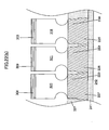
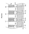
- FIG. 32 is a sectional view showing a solid-state imaging device according a second embodiment of the present invention.
- an oxide film 708 is formed on a silicon substrate 707.
- a signal line 706 is formed on the oxide film 708, and an island-shaped semiconductor is formed on the signal line 706.
- the island-shaped semiconductor comprises: an n+-type diffusion layer 705 formed as a bottom portion thereof and connected to the signal line; a p-type impurity-doped region 711 formed above and adjacent to the n+-type diffusion layer; a gate 704 connected to the p-type impurity-doped region through a dielectric film; a charge storage section 703 comprised of an n-type diffusion layer connected to the p-type impurity-doped region and adapted, in response to receiving light, to undergo a change in amount of electric charges therein; and a p+-type diffusion layer 702 formed above and adjacent to the p-type impurity-doped region and the n-type diffusion layer.
- a pixel selection line 701 comprised of a transparent conductive film is formed to be connected to a top of the p+-type diffusion layer which is a top portion of the island-shaped semiconductor.
- the gate is formed in such a manner that a part thereof is disposed inside a depression which is formed in a sidewall of the p-type impurity-doped region to have a square or rectangular shape in cross-section.
- a combination of the p+-type diffusion layer 702 and the n-type diffusion layer 703 functions as a photoelectric-conversion photodiode 709.
- An oxide film 710 is formed as an interlayer dielectric film.
- Each of the first and second embodiments shows a solid-state imaging device comprising an island-shaped semiconductor having a square or rectangular pillar shape.
- the solid-state imaging device may comprise an island-shaped semiconductor having a hexagonal pillar shape, as shown in FIG. 33 .
- the first embodiment shows a solid-state imaging device array in which a plurality of solid-state imaging devices each comprising an island-shaped semiconductor having a square or rectangular pillar shape are arranged in an n-row by m-column array (wherein each of n and m is an integer of 1 or more.) with respect to a substrate. For example, as shown in FIG.
- the 1st solid-state imaging device column consisting of three solid-state imaging devices 402, 403, 404 each comprising an island-shaped semiconductor having a hexagonal pillar shape
- the 2nd solid-state imaging device column consisting of three solid-state imaging devices 405, 406, 407 each comprising an island-shaped semiconductor having a hexagonal pillar shape
- the 3rd solid-state imaging device column consisting of three solid-state imaging devices 408, 409, 410 each comprising an island-shaped semiconductor having a hexagonal pillar shape
- the solid-state imaging device array may be arranged in a honeycomb pattern.
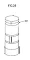
- each of the first and second embodiments shows a solid-state imaging device comprising an island-shaped semiconductor having a square or rectangular pillar shape.
- the solid-state imaging device may comprise an island-shaped semiconductor 501 having a circular pillar shape, as shown in FIG. 35 .
- the present invention provides a solid-state imaging device which comprises: a signal line formed on a substrate; an island-shaped semiconductor arranged on the signal line; and a pixel selection line connected to a top of the island-shaped semiconductor, wherein the island-shaped semiconductor includes: a first semiconductor layer formed as a bottom portion of the island-shaped semiconductor and connected to the signal line; a second semiconductor layer formed above and adjacent to the first semiconductor layer; a gate connected to the second semiconductor layer through a dielectric film; a charge storage section comprised of a third semiconductor layer connected to the second semiconductor layer and adapted, in response to receiving light, to undergo a change in amount of electric charges therein; and a fourth semiconductor layer formed above and adjacent to the second and third semiconductor layers, and wherein the pixel selection line is comprised of a transparent conductive film, and a part of the gate is disposed inside a depression formed in a sidewall of the second semiconductor layer.
- a combination of the third and fourth semiconductor layers, a combination of the second, third and fourth semiconductor layers, a combination of the first, second and third semiconductor layers, and a combination of the second and first semiconductor layers function, respectively, as the photoelectric-conversion photodiode, the amplification transistor, the reset transistor, and the diode in the aforementioned unit pixel.
- a metal for use in a conventional semiconductor production process such as aluminum or copper, reflects light. Thus, it is necessary to connect a line made of such a metal to a sidewall of the fourth semiconductor layer.
- a transparent conductive film such as indium tin oxide (ITO), zinc oxide (ZnO) or tin oxide (SnO 2 ) is used as the pixel selection line to allow the pixel selection line to be connected to a top of the fourth semiconductor layer.
- ITO indium tin oxide
- ZnO zinc oxide
- SnO 2 tin oxide
- a surface area of one pixel is a sum of an area of the photodiode, an area of the gate, and an area of a region between the devices.
- a part of the gate is disposed inside a depression formed in a sidewall of the second semiconductor layer, so that a surface area of one pixel can be reduced substantially to a sum of an area of the photodiode and an area of a region between the devices.
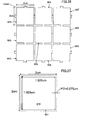
- FIG. 36 is a top plan view showing a solid-state imaging apparatus in which nine image sensors 601, 602, 603, 604, 605, 606, 607, 608, 609 each comprising the island-shaped semiconductor having a square pillar shape according to the present invention are arranged in a matrix array.
- FIG. 36 is a top plan view showing a solid-state imaging apparatus in which nine image sensors 601, 602, 603, 604, 605, 606, 607, 608, 609 each comprising the island-shaped semiconductor having a square pillar shape according to the present invention are arranged in a matrix array.
- FIG. 37 is an enlarged top plan view showing a light-receiving section 610 in one pixel of the solid-state imaging apparatus.
- F indicates a wiring rule.
- a 0.15 ⁇ m wiring-rule process is used on an assumption that a surface area per pixel is 2 ⁇ m ⁇ 2 ⁇ m.
- a surface area of the light-receiving section (photodiode) is 1.925 ⁇ m ⁇ 1.925 ⁇ m.
- a ratio of a surface area of a light-receiving section (photodiode) to an overall surface area of one pixel is 92.6%.
- a surface area of a unit pixel of an image sensor is largely occupied by a surface area of the photodiode, and it is possible to provide an image sensor having a sufficiently-large ratio of a surface area of a light-receiving section to an overall surface area of one pixel.
Landscapes
- Solid State Image Pick-Up Elements (AREA)
- Transforming Light Signals Into Electric Signals (AREA)
Applications Claiming Priority (2)
| Application Number | Priority Date | Filing Date | Title |
|---|---|---|---|
| PCT/JP2008/058412 WO2009133623A1 (fr) | 2008-05-02 | 2008-05-02 | Elément d’imagerie à semi-conducteur |
| PCT/JP2009/058629 WO2009133957A1 (fr) | 2008-05-02 | 2009-05-07 | Élément d’analyse d’image à l’état solide |
Publications (2)
| Publication Number | Publication Date |
|---|---|
| EP2290692A1 true EP2290692A1 (fr) | 2011-03-02 |
| EP2290692A4 EP2290692A4 (fr) | 2012-05-02 |
Family
ID=41254853
Family Applications (1)
| Application Number | Title | Priority Date | Filing Date |
|---|---|---|---|
| EP09738894A Withdrawn EP2290692A4 (fr) | 2008-05-02 | 2009-05-07 | Élément d analyse d image à l état solide |
Country Status (5)
| Country | Link |
|---|---|
| EP (1) | EP2290692A4 (fr) |
| KR (1) | KR101113905B1 (fr) |
| CN (1) | CN102017151B (fr) |
| TW (1) | TW200947691A (fr) |
| WO (2) | WO2009133623A1 (fr) |
Families Citing this family (17)
| Publication number | Priority date | Publication date | Assignee | Title |
|---|---|---|---|---|
| US8183628B2 (en) | 2007-10-29 | 2012-05-22 | Unisantis Electronics Singapore Pte Ltd. | Semiconductor structure and method of fabricating the semiconductor structure |
| US8598650B2 (en) | 2008-01-29 | 2013-12-03 | Unisantis Electronics Singapore Pte Ltd. | Semiconductor device and production method therefor |
| JP5317343B2 (ja) | 2009-04-28 | 2013-10-16 | ユニサンティス エレクトロニクス シンガポール プライベート リミテッド | 半導体装置及びその製造方法 |
| JP5356970B2 (ja) | 2009-10-01 | 2013-12-04 | ユニサンティス エレクトロニクス シンガポール プライベート リミテッド | 半導体装置 |
| WO2011111662A1 (fr) * | 2010-03-08 | 2011-09-15 | 日本ユニサンティスエレクトロニクス株式会社 | Dispositif de capture de semi-conducteurs |
| JP5054182B2 (ja) * | 2010-03-12 | 2012-10-24 | ユニサンティス エレクトロニクス シンガポール プライベート リミテッド | 固体撮像装置 |
| US8487357B2 (en) | 2010-03-12 | 2013-07-16 | Unisantis Electronics Singapore Pte Ltd. | Solid state imaging device having high sensitivity and high pixel density |
| JP5066590B2 (ja) | 2010-06-09 | 2012-11-07 | ユニサンティス エレクトロニクス シンガポール プライベート リミテッド | 半導体装置とその製造方法 |
| JP5087655B2 (ja) | 2010-06-15 | 2012-12-05 | ユニサンティス エレクトロニクス シンガポール プライベート リミテッド | 半導体装置及びその製造方法 |
| WO2012056586A1 (fr) * | 2010-10-29 | 2012-05-03 | 日本ユニサンティスエレクトロニクス株式会社 | Dispositif d'imagerie à semi-conducteurs |
| JP4769910B1 (ja) * | 2011-02-18 | 2011-09-07 | 日本ユニサンティスエレクトロニクス株式会社 | 固体撮像装置 |
| US8564034B2 (en) | 2011-09-08 | 2013-10-22 | Unisantis Electronics Singapore Pte. Ltd. | Solid-state imaging device |
| US8669601B2 (en) | 2011-09-15 | 2014-03-11 | Unisantis Electronics Singapore Pte. Ltd. | Method for producing semiconductor device and semiconductor device having pillar-shaped semiconductor |
| US8916478B2 (en) | 2011-12-19 | 2014-12-23 | Unisantis Electronics Singapore Pte. Ltd. | Method for manufacturing semiconductor device and semiconductor device |
| US8772175B2 (en) | 2011-12-19 | 2014-07-08 | Unisantis Electronics Singapore Pte. Ltd. | Method for manufacturing semiconductor device and semiconductor device |
| US8748938B2 (en) | 2012-02-20 | 2014-06-10 | Unisantis Electronics Singapore Pte. Ltd. | Solid-state imaging device |
| JP2025019860A (ja) * | 2023-07-28 | 2025-02-07 | ソニーセミコンダクタソリューションズ株式会社 | 光検出装置及び半導体装置 |
Family Cites Families (10)
| Publication number | Priority date | Publication date | Assignee | Title |
|---|---|---|---|---|
| JPS6417462A (en) * | 1987-07-11 | 1989-01-20 | Sony Corp | Read-only memory device |
| JPH01175775A (ja) * | 1987-12-29 | 1989-07-12 | Sharp Corp | 光駆動mos型半導体装置 |
| JPH0289368A (ja) * | 1988-09-27 | 1990-03-29 | Sony Corp | 固体撮像装置 |
| JP3621844B2 (ja) | 1999-02-24 | 2005-02-16 | シャープ株式会社 | 増幅型固体撮像装置 |
| DE19945136A1 (de) * | 1999-09-21 | 2001-04-12 | Infineon Technologies Ag | Vertikale Pixelzellen |
| JP3713418B2 (ja) * | 2000-05-30 | 2005-11-09 | 光正 小柳 | 3次元画像処理装置の製造方法 |
| JP4714998B2 (ja) | 2001-02-14 | 2011-07-06 | ソニー株式会社 | 固体撮像素子 |
| JP3899236B2 (ja) * | 2001-02-16 | 2007-03-28 | シャープ株式会社 | イメージセンサの製造方法 |
| JP4218894B2 (ja) | 2004-07-08 | 2009-02-04 | シャープ株式会社 | 固体撮像装置およびその製造方法 |
| KR100734313B1 (ko) * | 2006-02-09 | 2007-07-02 | 삼성전자주식회사 | 수직 채널을 갖는 반도체 소자 및 그 제조방법 |
-
2008
- 2008-05-02 WO PCT/JP2008/058412 patent/WO2009133623A1/fr not_active Ceased
-
2009
- 2009-04-29 TW TW098114145A patent/TW200947691A/zh unknown
- 2009-05-07 CN CN2009801158772A patent/CN102017151B/zh not_active Expired - Fee Related
- 2009-05-07 EP EP09738894A patent/EP2290692A4/fr not_active Withdrawn
- 2009-05-07 KR KR1020107024780A patent/KR101113905B1/ko not_active Expired - Fee Related
- 2009-05-07 WO PCT/JP2009/058629 patent/WO2009133957A1/fr not_active Ceased
Also Published As
| Publication number | Publication date |
|---|---|
| KR101113905B1 (ko) | 2012-02-29 |
| WO2009133623A1 (fr) | 2009-11-05 |
| CN102017151B (zh) | 2012-10-10 |
| EP2290692A4 (fr) | 2012-05-02 |
| KR20110005707A (ko) | 2011-01-18 |
| CN102017151A (zh) | 2011-04-13 |
| WO2009133957A1 (fr) | 2009-11-05 |
| TW200947691A (en) | 2009-11-16 |
Similar Documents
| Publication | Publication Date | Title |
|---|---|---|
| EP2290692A1 (fr) | Élément d analyse d image à l état solide | |
| US8097907B2 (en) | Solid-state imaging device | |
| TWI443810B (zh) | 固態攝像裝置,及固態攝像元件的製造方法 | |
| US11081514B2 (en) | Image sensors and methods of forming the same | |
| US9054003B2 (en) | Image sensors and methods of fabricating the same | |
| KR101529094B1 (ko) | 고체 촬상 소자 및 카메라 | |
| US10998358B2 (en) | Image sensor including dummy isolation structure | |
| JP2009038309A (ja) | 固体撮像素子およびその製造方法、電子情報機器 | |
| WO2014141900A1 (fr) | Élément de capture d'image à semi-conducteurs, procédé permettant de produire ce dernier, et équipement électronique | |
| US20100200731A1 (en) | Solid-state imaging device | |
| CN104882460A (zh) | 具有包括负电荷材料的深沟槽的图像传感器及其制造方法 | |
| US11183526B2 (en) | Image sensor | |
| US20120077301A1 (en) | Image sensor and method of fabricating the same | |
| US9583527B1 (en) | Contact resistance reduction | |
| US8164127B2 (en) | Image sensor including a pixel cell having an epitaxial layer, system having the same, and method of forming a pixel cell | |
| US20110001207A1 (en) | Solid state image sensor and manufacturing method thereof | |
| US20140015026A1 (en) | Image sensors including well regions of different concentrations | |
| JP5283235B2 (ja) | 固体撮像素子 | |
| US20250248162A1 (en) | Image sensor | |
| KR100792335B1 (ko) | 이미지 센서 및 이의 제조 방법 | |
| JP5350795B2 (ja) | 固体撮像素子 | |
| JP2013138222A (ja) | 固体撮像素子 | |
| JP2007012677A (ja) | 固体撮像素子およびその製造方法 |
Legal Events
| Date | Code | Title | Description |
|---|---|---|---|
| PUAI | Public reference made under article 153(3) epc to a published international application that has entered the european phase |
Free format text: ORIGINAL CODE: 0009012 |
|
| 17P | Request for examination filed |
Effective date: 20101125 |
|
| AK | Designated contracting states |
Kind code of ref document: A1 Designated state(s): AT BE BG CH CY CZ DE DK EE ES FI FR GB GR HR HU IE IS IT LI LT LU LV MC MK MT NL NO PL PT RO SE SI SK TR |
|
| AX | Request for extension of the european patent |
Extension state: AL BA RS |
|
| DAX | Request for extension of the european patent (deleted) | ||
| RAP1 | Party data changed (applicant data changed or rights of an application transferred) |
Owner name: UNISANTIS ELECTRONICS SINGAPORE PTE. LTD. |
|
| A4 | Supplementary search report drawn up and despatched |
Effective date: 20120402 |
|
| RIC1 | Information provided on ipc code assigned before grant |
Ipc: H01L 27/146 20060101AFI20120327BHEP |
|
| 17Q | First examination report despatched |
Effective date: 20120626 |
|
| RAP1 | Party data changed (applicant data changed or rights of an application transferred) |
Owner name: UNISANTIS ELECTRONICS SINGAPORE PTE. LTD. |
|
| STAA | Information on the status of an ep patent application or granted ep patent |
Free format text: STATUS: THE APPLICATION IS DEEMED TO BE WITHDRAWN |
|
| 18D | Application deemed to be withdrawn |
Effective date: 20141202 |