EP2290723A2 - Photoelektrisches Umwandlungselement und Abbildungsvorrichtung - Google Patents
Photoelektrisches Umwandlungselement und Abbildungsvorrichtung Download PDFInfo
- Publication number
- EP2290723A2 EP2290723A2 EP10174286A EP10174286A EP2290723A2 EP 2290723 A2 EP2290723 A2 EP 2290723A2 EP 10174286 A EP10174286 A EP 10174286A EP 10174286 A EP10174286 A EP 10174286A EP 2290723 A2 EP2290723 A2 EP 2290723A2
- Authority
- EP
- European Patent Office
- Prior art keywords
- photoelectric conversion
- conversion element
- electrode
- layer
- pixel electrode
- Prior art date
- Legal status (The legal status is an assumption and is not a legal conclusion. Google has not performed a legal analysis and makes no representation as to the accuracy of the status listed.)
- Granted
Links
Images


Classifications
-
- B—PERFORMING OPERATIONS; TRANSPORTING
- B82—NANOTECHNOLOGY
- B82Y—SPECIFIC USES OR APPLICATIONS OF NANOSTRUCTURES; MEASUREMENT OR ANALYSIS OF NANOSTRUCTURES; MANUFACTURE OR TREATMENT OF NANOSTRUCTURES
- B82Y10/00—Nanotechnology for information processing, storage or transmission, e.g. quantum computing or single electron logic
-
- H—ELECTRICITY
- H10—SEMICONDUCTOR DEVICES; ELECTRIC SOLID-STATE DEVICES NOT OTHERWISE PROVIDED FOR
- H10K—ORGANIC ELECTRIC SOLID-STATE DEVICES
- H10K30/00—Organic devices sensitive to infrared radiation, light, electromagnetic radiation of shorter wavelength or corpuscular radiation
- H10K30/20—Organic devices sensitive to infrared radiation, light, electromagnetic radiation of shorter wavelength or corpuscular radiation comprising organic-organic junctions, e.g. donor-acceptor junctions
-
- H—ELECTRICITY
- H10—SEMICONDUCTOR DEVICES; ELECTRIC SOLID-STATE DEVICES NOT OTHERWISE PROVIDED FOR
- H10K—ORGANIC ELECTRIC SOLID-STATE DEVICES
- H10K30/00—Organic devices sensitive to infrared radiation, light, electromagnetic radiation of shorter wavelength or corpuscular radiation
- H10K30/80—Constructional details
- H10K30/81—Electrodes
- H10K30/82—Transparent electrodes, e.g. indium tin oxide [ITO] electrodes
-
- H—ELECTRICITY
- H10—SEMICONDUCTOR DEVICES; ELECTRIC SOLID-STATE DEVICES NOT OTHERWISE PROVIDED FOR
- H10K—ORGANIC ELECTRIC SOLID-STATE DEVICES
- H10K85/00—Organic materials used in the body or electrodes of devices covered by this subclass
- H10K85/20—Carbon compounds, e.g. carbon nanotubes or fullerenes
- H10K85/211—Fullerenes, e.g. C60
-
- H—ELECTRICITY
- H10—SEMICONDUCTOR DEVICES; ELECTRIC SOLID-STATE DEVICES NOT OTHERWISE PROVIDED FOR
- H10K—ORGANIC ELECTRIC SOLID-STATE DEVICES
- H10K85/00—Organic materials used in the body or electrodes of devices covered by this subclass
- H10K85/60—Organic compounds having low molecular weight
- H10K85/631—Amine compounds having at least two aryl rest on at least one amine-nitrogen atom, e.g. triphenylamine
- H10K85/633—Amine compounds having at least two aryl rest on at least one amine-nitrogen atom, e.g. triphenylamine comprising polycyclic condensed aromatic hydrocarbons as substituents on the nitrogen atom
-
- H—ELECTRICITY
- H10—SEMICONDUCTOR DEVICES; ELECTRIC SOLID-STATE DEVICES NOT OTHERWISE PROVIDED FOR
- H10K—ORGANIC ELECTRIC SOLID-STATE DEVICES
- H10K85/00—Organic materials used in the body or electrodes of devices covered by this subclass
- H10K85/60—Organic compounds having low molecular weight
- H10K85/631—Amine compounds having at least two aryl rest on at least one amine-nitrogen atom, e.g. triphenylamine
- H10K85/636—Amine compounds having at least two aryl rest on at least one amine-nitrogen atom, e.g. triphenylamine comprising heteroaromatic hydrocarbons as substituents on the nitrogen atom
-
- H—ELECTRICITY
- H10—SEMICONDUCTOR DEVICES; ELECTRIC SOLID-STATE DEVICES NOT OTHERWISE PROVIDED FOR
- H10K—ORGANIC ELECTRIC SOLID-STATE DEVICES
- H10K85/00—Organic materials used in the body or electrodes of devices covered by this subclass
- H10K85/60—Organic compounds having low molecular weight
- H10K85/649—Aromatic compounds comprising a hetero atom
- H10K85/652—Cyanine dyes
-
- H—ELECTRICITY
- H10—SEMICONDUCTOR DEVICES; ELECTRIC SOLID-STATE DEVICES NOT OTHERWISE PROVIDED FOR
- H10K—ORGANIC ELECTRIC SOLID-STATE DEVICES
- H10K85/00—Organic materials used in the body or electrodes of devices covered by this subclass
- H10K85/60—Organic compounds having low molecular weight
- H10K85/649—Aromatic compounds comprising a hetero atom
- H10K85/654—Aromatic compounds comprising a hetero atom comprising only nitrogen as heteroatom
-
- H—ELECTRICITY
- H10—SEMICONDUCTOR DEVICES; ELECTRIC SOLID-STATE DEVICES NOT OTHERWISE PROVIDED FOR
- H10K—ORGANIC ELECTRIC SOLID-STATE DEVICES
- H10K85/00—Organic materials used in the body or electrodes of devices covered by this subclass
- H10K85/60—Organic compounds having low molecular weight
- H10K85/649—Aromatic compounds comprising a hetero atom
- H10K85/657—Polycyclic condensed heteroaromatic hydrocarbons
-
- H—ELECTRICITY
- H10—SEMICONDUCTOR DEVICES; ELECTRIC SOLID-STATE DEVICES NOT OTHERWISE PROVIDED FOR
- H10K—ORGANIC ELECTRIC SOLID-STATE DEVICES
- H10K30/00—Organic devices sensitive to infrared radiation, light, electromagnetic radiation of shorter wavelength or corpuscular radiation
- H10K30/50—Photovoltaic [PV] devices
-
- Y—GENERAL TAGGING OF NEW TECHNOLOGICAL DEVELOPMENTS; GENERAL TAGGING OF CROSS-SECTIONAL TECHNOLOGIES SPANNING OVER SEVERAL SECTIONS OF THE IPC; TECHNICAL SUBJECTS COVERED BY FORMER USPC CROSS-REFERENCE ART COLLECTIONS [XRACs] AND DIGESTS
- Y02—TECHNOLOGIES OR APPLICATIONS FOR MITIGATION OR ADAPTATION AGAINST CLIMATE CHANGE
- Y02E—REDUCTION OF GREENHOUSE GAS [GHG] EMISSIONS, RELATED TO ENERGY GENERATION, TRANSMISSION OR DISTRIBUTION
- Y02E10/00—Energy generation through renewable energy sources
- Y02E10/50—Photovoltaic [PV] energy
- Y02E10/548—Amorphous silicon PV cells
-
- Y—GENERAL TAGGING OF NEW TECHNOLOGICAL DEVELOPMENTS; GENERAL TAGGING OF CROSS-SECTIONAL TECHNOLOGIES SPANNING OVER SEVERAL SECTIONS OF THE IPC; TECHNICAL SUBJECTS COVERED BY FORMER USPC CROSS-REFERENCE ART COLLECTIONS [XRACs] AND DIGESTS
- Y02—TECHNOLOGIES OR APPLICATIONS FOR MITIGATION OR ADAPTATION AGAINST CLIMATE CHANGE
- Y02E—REDUCTION OF GREENHOUSE GAS [GHG] EMISSIONS, RELATED TO ENERGY GENERATION, TRANSMISSION OR DISTRIBUTION
- Y02E10/00—Energy generation through renewable energy sources
- Y02E10/50—Photovoltaic [PV] energy
- Y02E10/549—Organic PV cells
Definitions
- the present invention relates to a photoelectric conversion element and an imaging device.
- a solid-state imaging apparatus (a so-called CCD sensor or CMOS sensor) is widely known as an image sensor used in a digital still camera, a digital video camera, a cell-phone camera, an endoscopic camera and the like.
- CCD sensor a so-called CCD sensor or CMOS sensor
- CMOS sensor CMOS sensor
- photodiode-containing pixels are arranged on a semiconductor substrate such as silicon chip, and signal charges corresponding to photoelectrons generated in the photodiode of each pixel are acquired through a CCD or CMOS reading circuit.
- JP-B-1-34509 (the term "JP-B” as used herein means an "examined published Japanese patent application”) has proposed a so-called stacked solid-state imaging apparatus where a photoelectric conversion layer is stacked above a semiconductor substrate having formed thereon respective circuits and interconnections and the aperture ratio is thereby increased.
- the imaging apparatus has a configuration such that a large number of photoelectric conversion elements each containing a pixel electrode formed on a semiconductor substrate, a photoelectric conversion layer formed on the pixel electrode and a counter electrode formed on the photoelectric conversion layer are arranged on a plane parallel to the semiconductor substrate.
- the pixel electrode and the counter electrode are sometimes referred to as a lower electrode and an upper electrode, respectively.
- an exciton generated in the photoelectric conversion layer upon application of a bias voltage between the pixel electrode and the counter electrode is dissociated into electrons and holes, and signals in proportion to electron or hole charges moved to the pixel electrode according to the bias voltage are acquired through a CCD or CMOS reading circuit provided in the semiconductor substrate.
- the photoelectric conversion element is a device where an electric charge is produced in a photoelectric conversion layer according to light incident from the side of a transparent electrode having light transmittance out of a pair of electrodes and the produced electric charge is read as a signal charge from an electrode.
- a photoelectric conversion element those described in JP-A-2008-72090 (the term "JP-A” as used herein means an "unexamined published Japanese patent application") and JP-A-2007-273945 are known.
- the photoelectric conversion layer is composed of an organic semiconductor, making it possible to form a thin photoelectric conversion layer while ensuring a large absorption coefficient, whereby less diffusion of an electric charge into the adjacent pixel and reduction in the optical color mixing and electrical color mixing (crosstalk) can be achieved.
- JP-A-2008-72090 describes a photoelectric conversion element where a pixel electrode is produced on a transparent substrate such as glass and a transparent electrically conductive oxide (TCO) is used for the material of the pixel electrode.
- TCO transparent electrically conductive oxide
- the configuration of providing a pixel electrode composed of TCO or the like on a transparent substrate such as glass is found to suffer from a decrease in the adherence between the pixel electrode and an organic layer containing a photoelectric conversion layer.
- difference in the coefficient of thermal expansion between the pixel electrode and the organic layer causes the dark current to increase due to heat in a heat treatment at the production, which gives rise to serious deterioration of S/N, and in this respect, there is room for improvement.
- An object of the present invention is to provide a photoelectric conversion element and an imaging device each succeeded in enhancing the adherence between a pixel electrode and an organic material and suppressing the increase of dark current.
- a photoelectric conversion element comprising, in the following order, a substrate, a lower electrode, an organic layer containing a photoelectric conversion layer, and an upper electrode containing a transparent electrode material, wherein the lower electrode contains titanium nitride.
- the present inventors have found that when a photoelectric conversion element having, between a lower electrode and an upper electrode, an organic layer containing a photoelectric conversion layer is in a configuration of providing a lower electrode containing titanium nitride on the substrate, the adherence between the lower electrode and the organic layer containing a photoelectric conversion layer is enhanced as compared with a case of producing TCO on a glass substrate.
- a photoelectric conversion element and an imaging device each succeeded in enhancing the adherence between a pixel electrode and an organic material and suppressing the increase of dark current can be provided.
- the photoelectric conversion element comprising, in the following order, a substrate, a lower electrode, an organic layer containing a photoelectric conversion layer, and a lower electrode containing a transparent electrode material, which is a photoelectric conversion element having a configuration in which the lower electrode contains titanium nitride, the adherence between the lower electrode and the organic layer can be enhanced and the increase of dark current can be suppressed.
- the configuration of the photoelectric conversion element is specifically described.
- the material of the lower electrode As for the material of the lower electrode, a metal such as aluminum and gold or a metal oxide typified by ITO is generally used. In this configuration, titanium nitride (TiN) is further contained in the lower electrode, whereby flatness and adherence are improved and the dark current at heating is significantly suppressed.
- TiN titanium nitride
- the content of titanium nitride in the lower electrode is, on a weight basis, preferably 70% or more, more preferably 90% or more. If the content of titanium nitride is less than 70%, the electrical conductivity decreases.
- Titanium oxide is often contained due to introduction of oxygen into titanium nitride.
- the content of titanium oxide is preferably 10% or less, more preferably 5% or less. If the content of titanium oxide exceeds 10%, the electrical conductivity decreases.
- the stoichiometric composition of titanium nitride is Ti 3 N 4 , but from an analytical viewpoint, this stoichiometric composition can be changed. It has been found that the ratio of N atom to Ti atom is correlated with the adherence to organic layer and the work function. In consideration of adherence to the organic layer and work function, the ratio is preferably from 1 to 3.9 mol of N atom per 3 mol of Ti atom, more preferably from 2 to 3.8 mol of N atom per 3 mol of Ti atom.
- the photoelectric conversion element of this configuration example is preferably configured to let light be incident from the upper electrode side, let electrons generated in the photoelectric conversion layer be collected on the upper electrode side, and let holes be collected on the lower electrode side. At this time, a built-in electric field is caused to be applied due to difference between the work function on the upper electrode side and the work function on the lower electrode side.
- the material used for the lower electrode preferably has a work function of about 4.6 eV or more, more preferably 4.7 eV or more.
- the work function can be made to be 4.6 eV or more by the compositional ratio between nitrogen and titanium of titanium nitride in the lower electrode.
- the method for depositing the titanium nitride-containing lower electrode includes a vapor deposition method, a sputtering method, a CVD method and the like, but it is most preferred to use a CVD method based on the compositional ratio between nitrogen and titanium of titanium nitride in the lower electrode.
- the lower electrode is a plurality of pixel electrodes divided for each pixel, a pronounced effect of enhancing the adherence of the plurality of pixel electrodes to the organic layer is brought out.
- the lower electrode takes a configuration where in planar view (a state of viewing the substrate surface from the light indent side), a plurality of square pixel electrodes are arranged like tiles according to the positions of pixels.
- the plurality of pixel electrodes are one-dimensionally or two-dimensionally arranged but is preferably two-dimensionally arranged.
- the side length of a pixel becomes less than 2 ⁇ m, particularly about 1 ⁇ m, there arises practically no problem.
- the distance between pixel electrodes is preferably 1.0 ⁇ m or less, more preferably 0.3 ⁇ m or less.
- the thickness of the pixel electrode is related to the electric resistance and flatness and for reducing the electric resistance, the thickness needs to be increased, which, however, brings about a decrease in the flatness.
- the thickness of the pixel electrode is preferably 100 nm or less, more preferably 30 nm or less.
- the surface roughness of the pixel electrode is related to the adherence and when the surface of the pixel electrode is rough, joining at the interface between the pixel electrode and the organic layer becomes weak and the adherence decreases. It has been found that the flatness is improved by containing titanium nitride. Improved flatness enables enhancing the adherence and obtaining a remarkable effect of suppressing an increase of dark current at heating.
- the average surface roughness of the pixel electrode is preferably 1 nm or less, more preferably 0.6 nm or less.
- the tilt angle in the edge part of the pixel electrode with respect to the substrate surface is also related to the adherence. It has been confirmed that when this tilt angle is an obtuse angle, the adherence decreases.
- the tilt angle in the edge part of the pixel electrode is preferably from 10 to 80°, more preferably from 20 to 80°, with respect to the substrate surface.
- the method for pattering the pixel electrode includes two methods, that is, wet etching which is an anisotropic etching using chemicals, and dry etching which is an isotropic etching using plasma.
- wet etching since a solution is used, etching cannot be performed isotropically, and the tilt angle in the edge part of the pixel electrode can be hardly made acute.
- patterning is preferably performed by dry etching that can effect isotropic etching and make the tilt angle acute.
- the substrate is composed of single-crystal silicon.
- an insulating layer is formed on the surface in the lower electrode side of the substrate. It has been found that by using a substrate containing single-crystal silicon, the average surface roughness on the pixel electrode is improved and this enables enhancing the adherence and significantly suppressing the dark current at heating.
- Silicon oxide is preferably contained in the insulating layer, and it is more preferred to contain silicon nitride in the insulating layer.
- the organic layer is composed of a charge blocking layer for suppressing injection of an electric charge from the lower electrode, and a photoelectric conversion layer.
- the film thickness of the organic layer is preferably 1 ⁇ m or less, more preferably 800 nm or less, still more preferably 600 nm or less, and most preferably 400 nm or less.
- the molecular weight of the organic compound in the organic layer in direct contact with the lower electrode is preferably from 400 to 1,300, more preferably from 450 to 1,200, still more preferably from 500 to 1,100.
- the photoelectric conversion layer contains a p-type organic semiconductor and an n-type organic semiconductor.
- the p-type organic semiconductor and the n-type organic semiconductor are joined to form a donor-acceptor interface, whereby the exciton dissociation efficiency can be increased.
- the photoelectric conversion layer in the configuration of a p-type organic semiconductor and an n-type organic semiconductor being joined exhibits a high photoelectric conversion efficiency.
- a photoelectric conversion layer where a p-type organic semiconductor and an n-type organic semiconductor are mixed is preferred, because the joint interface is increased and the photoelectric conversion efficiency is enhanced.
- the p-type organic semiconductor is a donor-type organic semiconductor (compound) and indicates an organic compound having a property of readily donating an electron, mainly typified by a hole-transporting organic compound. More specifically, this is an organic compound having a smaller ionization potential when two organic materials are used in contact with each other. Accordingly, the donor-type organic compound may be any organic compound as long as it is an organic compound having an electron donating property.
- Examples of the compound which can be used include a triarylamine compound, a benzidine compound, a pyrazoline compound, a styrylamine compound, a hydrazone compound, a triphenylmethane compound, a carbazole compound, a polysilane compound, a thiophene compound, a phthalocyanine compound, a cyanine compound, a merocyanine compound, an oxonol compound, a polyamine compound, an indole compound, a pyrrole compound, a pyrazole compound, a polyarylene compound, a fused aromatic carbocyclic compound (e.g., naphthalene derivative, anthracene derivative, phenanthrene derivative, tetracene derivative, pyrene derivative, perylene derivative, fluoranthene derivative), and a metal complex having a nitrogen-containing heterocyclic compound as a ligand.
- the donor-type organic semiconductor is not limited to these
- the n-type organic semiconductor is an acceptor-type organic semiconductor (compound) and indicates an organic compound having a property of readily accepting an electron, mainly typified by an electron-transporting organic compound. More specifically, the n-type organic semiconductor is an organic compound having a larger electron affinity when two organic compounds are used in contact with each other. Accordingly, for the acceptor-type organic compound, any organic compound can be used as long as it is an organic compound having an electron accepting property.
- Examples thereof include a fused aromatic carbocyclic compound (e.g., naphthalene derivative, anthracene derivative, phenanthrene derivative, tetracene derivative, pyrene derivative, perylene derivative, fluoranthene derivative), a 5- to 7-membered heterocyclic compound containing a nitrogen atom, an oxygen atom or a sulfur atom (e.g., pyridine, pyrazine, pyrimidine, pyridazine, triazine, quinoline, quinoxaline, quinazoline, phthalazine, cinnoline, isoquinoline, pteridine, acridine, phenazine, phenanthroline, tetrazole, pyrazole, imidazole, thiazole, oxazole, indazole, benzimidazole, benzotriazole, benzoxazole, benzothiazole, carbazole, purine, triazo
- any organic dye may be used, but preferred examples thereof include cyanine dyes, styryl dyes, hemicyanine dyes, merocyanine dyes (including zeromethine merocyanine (simple merocyanine)), trinuclear merocyanine dyes, tetranuclear merocyanine dyes, rhodacyanine dyes, complex cyanine dyes, complex merocyanine dyes, alopolar dyes, oxonol dyes, hemioxonol dyes, squarylium dyes, croconium dyes, azamethine dyes, coumarin dyes, arylidene dyes, anthraquinone dyes, triphenylmethane dyes, azo dyes, azomethine dyes, spiro compound, metallocene dyes, fluorenone dyes, flugide dye
- a fullerene or fullerene derivative excellent in the electron transportability is preferably used.
- the fullerene indicates fullerene C 60 , fullerene C 70 , fullerene C 76 , fullerene C 78 , fullerene C 80 , fullerene C 82 , fullerene C 84 , fullerene C 90 , fullerene C 96 , fullerene C 240 , fullerene C 540 , a mixed fullerene or a fullerene nanotube, and the fullerene derivative indicates a compound obtained by adding a substituent to such a fullerene.
- the substituent of the fullerene derivative is preferably an alkyl group, an aryl group or a heterocyclic group.
- the alkyl group is preferably an alkyl group having carbon number of 1 to 12, and the aryl group and heterocyclic group are preferably a benzene ring, a naphthalene ring, an anthracene ring, a phenanthrene ring, a fluorene ring, a triphenylene ring, a naphthacene ring, a biphenyl ring, a pyrrole ring, a furan ring, a thiophene ring, an imidazole ring, an oxazole ring, a thiazole ring, a pyridine ring, a pyrazine ring, a pyrimidine ring, a pyridazine ring, an indolizine ring, an indole ring,
- these may further have a substituent, and the substituent may combine, if possible, to form a ring.
- these groups each may have a plurality of substituents, and the substituents may be the same or different. Also, a plurality of substituents may combine, if possible, to form a ring.
- the fullerene or fullerene derivative is preferably contained in an amount of 40% or more by volume in the photoelectric conversion layer.
- the fullerene or fullerene derivative is contained in an excessively large amount, the proportion of the p-type semiconductor decreases and the joint interface becomes small, which leads to a decrease in the exciton dissociation efficiency.
- the photoelectric conversion element when the triarylamine compound described in Japanese Patent 4,213,832 is used as the p-type organic semiconductor mixed together with the fullerene or fullerene derivative, the photoelectric conversion element can exhibit a high SN ratio, and this is more preferred.
- a structure having a substituent at the P-position of the triarylamine structure is preferred.
- the substituent may combine, if possible, to form a ring.
- the compound may have a plurality of substituents, and these substituents may be the same or different. Also, the plurality of substituents may combine, if possible, to form a ring.
- the content of the fullerene or fullerene derivative in the photoelectric conversion layer is preferably 85% or less by volume.
- an electron-donating organic material can be used.
- the material which can be used include, as a low molecular material, an aromatic diamine compound such as N,N'-bis(3-methylphenyl)-(1,1'-biphenyl)-4,4'-diamine (TPD) and 4,4'-bis[N-(naphthyl)-N-phenyl-amino]biphenyl ( ⁇ -NPD), oxazole, oxadiazole, triazole, imidazole, imidazolone, a stilbene derivative, a pyrazoline derivative, tetrahydroimidazole, a polyarylalkane, butadiene, 4,4',4"-tris(N-(3-methylphenyl)N-phenylamino)triphenylamine (m-MTDATA), a porphyrin compound such as porphin, copper tetraphenylporphin, phthalocyanine
- a polymer material a polymer such as phenylenevinylene, fluorene, carbazole, indole, pyrene, pyrrole, picolin, thiophene, acetylene and diacetylene, and a derivative thereof can be used.
- a compound having a sufficient hole transportability may be used even if it is not an electron-donating compound.
- An inorganic material may also be used for the charge blocking layer.
- An inorganic material is generally larger in the dielectric constant than an organic material and therefore, when used for the charge blocking layer 15a, this allows for supply of a large amount of voltages to the photoelectric conversion layer, as a result, the photoelectric conversion efficient can be elevated.
- Examples of the material that can work out to the charge blocking layer include calcium oxide, chromium oxide, chromium copper oxide, manganese oxide, cobalt oxide, nickel oxide, copper oxide, gallium copper oxide, strontium copper oxide, niobium oxide, molybdenum oxide, indium copper oxide, indium silver oxide and iridium oxide. More preferred examples include cerium oxide and tin oxide.
- the charge blocking layer may be composed of a plurality of layers.
- the layer adjacent to the photoelectric conversion layer is preferably a layer composed of the same material as the p-type organic semiconductor contained in the photoelectric conversion layer.
- Use of the same p-type organic semiconductor also for the charge blocking layer makes it possible to prevent the formation of an intermediate level at the interface between the photoelectric conversion layer and the layer adjacent thereto and more reduce the dark current.
- the layer may be a layer composed of an inorganic material, and in the case of a plurality of layers, one layer or two or more layers can be a layer composed of an inorganic material.
- the upper electrode is preferably composed of a transparent electrically conductive film.
- the material therefor include a metal, a metal oxide, a metal nitride, a metal sulfide, an organic electrically conductive compound, and a mixture thereof.
- an electrically conductive metal oxide such as tin oxide, zinc oxide, indium oxide, indium tin oxide (ITO), indium zinc oxide (IZO), indium tungsten oxide (IWO) and titanium oxide
- a metal nitride such as titanium nitride
- a metal such as gold (Au), platinum (Pt), silver (Ag), chromium (Cr), nickel (Ni) and aluminum (Al)
- Au gold
- silver Au
- Cr chromium
- Ni nickel
- Al aluminum
- a mixture or laminate of such a metal and such an electrically conductive metal oxide an organic electrically conductive compound such as polyaniline, polythiophene and polypyrrole, and a laminate thereof with ITO.
- the material of the transparent electrically conductive film is preferably a transparent electrically conductive oxide, specifically, any one material of ITO, IZO, tin oxide, antimony-doped tin oxide (ATO), fluorine-doped tin oxide (FTO), zinc oxide, antimony-doped zinc oxide (AZO) and gallium-doped zinc oxide (GZO).
- the material as the transparent electrically conductive oxide is more preferably ITO.
- the film thickness of the upper electrode is preferably large so as to reduce the electric resistance.
- the method for depositing the upper electrode is preferably a sputtering method and when the upper electrode is deposited to a large film thickness, this takes a long time and causes great damage to the organic layer just below the upper electrode.
- the film thickness is preferably from 3 to 100 nm, more preferably from 5 to 50 nm.
- the surface resistance of the upper electrode is, in the case of CMOS reading circuit, preferably 10 K ⁇ /sq or less, more preferably 1 K ⁇ /sq or less, and in the case of CCD reading circuit, preferably 1 K ⁇ /sq or less, more preferably 0.1 K ⁇ /sq or less.
- Fig. 1 is a cross-sectional view schematically showing one configuration example of the photoelectric conversion element.
- the photoelectric conversion element shown in Fig. 1 is in the configuration where a substrate 101 composed of single-crystal silicon (Si), an insulating layer 102 formed on the substrate 101, a pixel electrode 104 provided on the insulating layer 102, a charge blocking layer 15a, a photoelectric conversion layer 15, a transparent electrode 108 functioning as an upper electrode are stacked in this order.
- the photoelectric conversion layer 15 and the charge blocking layer 15a are collectively referred to as the organic layer.
- a protective film 119 composed of silicon oxide (SiO) or the like is formed.
- the photoelectric conversion element shown in Fig. 1 is designed to let light be incident from above the transparent upper electrode 108.
- a bias voltage is applied between the lower electrode 104 and the upper electrode 108 so that out of electric charges (a hole and an electron) generated in the photoelectric conversion layer 15, the hole can move to the upper electrode 108 and the electron can move to the lower electrode 104.
- the upper electrode 108 is a hole trapping electrode
- the lower electrode 104 is an electron trapping electrode.
- the insulating layer 102 is in the configuration where a thermal oxide film (Th-SiO 2 ) 102a and an interlayer insulating layer (IMD: Inter Metal Dielectric) 102b are stacked in this order on the substrate 101.
- IMD Inter Metal Dielectric
- the configuration of the insulating layer 102 is not limited thereto.
- the configuration of the photoelectric conversion element is not limited to that described above.
- the upper electrode 108 may serve as an electron trapping electrode
- the lower electrode 104 may serve as a hole trapping electrode
- a layer other than the lower electrode 104, the photoelectric conversion layer 15 and the upper electrode 108 may be further provided.
- the charge blocking layer 15a may be provided between the photoelectric conversion layer 15 and the upper electrode 108, or the charge blocking layer 15a may be provided between the pixel electrode 104 and the photoelectric conversion layer 15 and also between the upper electrode 108 and the photoelectric conversion layer 15.
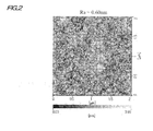
- Figs. 2 and 3 each is an image obtained by photographing the surface of the lower electrode with an atomic force microscope (AFM).
- AFM atomic force microscope
- an insulating layer is formed on a substrate containing single-crystal silicon, and a lower electrode is formed on the insulating layer.
- the surface roughness (Ra) of the lower electrode shown in Fig. 2 is 0.60 nm
- the surface roughness (Ra) of the lower electrode shown in Fig. 3 is 1.04 nm, revealing that the lower electrode shown in Fig. 2 is smaller in the surface roughness, that is, more flat, than the lower electrode of Fig. 3 .
- the surface roughness of the lower electrode is smaller, that is, as the lower electrode is more flat, the adherence to the organic layer in contact with the lower electrode is more enhanced.
- Fig. 4 is a schematic view showing the cross-section of the lower electrode.
- the lower electrode 104 is provided on a silicon substrate 101 through an insulating layer 102.
- the charge blocking layer 15a of the organic layer is stacked on the insulating layer 102 to cover the lower electrode 104.
- a tilted surface 104a is provided in the edge part of the lower electrode 104.
- the tilted surface 104a is tilted at an angle A with respect to the surface (containing the insulating layer 102) of the substrate 101. This angle A is defined as the tilt angle in the edge part of the lower electrode.
- Figs. 5 and 6 each is an image obtained by photographing the edge part of the pixel electrode in the photoelectric conversion element with a scanning electron microscope (SEM). Incidentally, in Figs. 5 and 6 , the edge part of one pixel electrode out of a plurality of pixel electrodes formed by dividing the lower electrode for each pixel is shown.
- SEM scanning electron microscope
- an insulating layer is formed on a substrate, and a pixel electrode is formed by dry etching on the insulating layer.
- an insulating layer is formed on a silicon substrate, and a pixel electrode is formed by dry etching on the insulating layer.
- the blackened region indicates the cross-sectional portion of the organic layer, and the gray region lighter than the region above indicates the cross-sectional portion of the substrate and the pixel electrode provided on the substrate.
- the edge part of the pixel electrode shown in Fig. 5 is tilted at about 50° with respect to the surface of the substrate.
- the edge part of the pixel electrode shown in Fig. 6 is tilted at about 20° with respect to the surface of the substrate.
- the edge part of the pixel electrode is configured in a nearly step-shaped manner to have a tilt angle of 50° or more with respect to the substrate as shown in Fig. 5 , the adherence between the pixel electrode and the organic layer is enhanced as compared with a configuration in which the entire pixel electrode forms a gentle slope with respect to the substrate as shown in Fig. 6 .
- An insulating layer containing silicon oxide was formed on a silicon substrate to a film thickness of 200 nm and on the insulating layer, titanium nitride (3.8 mol of N atom per 3 mol of Ti atom) was patterned by dry etching to a thickness of 100 nm to form a pixel electrode.
- the compound represented by chemical formula 1 molecular weight: 794
- the compounds represented by chemical formulae 4, 5 and 6 were co-deposited to a thickness of 400 nm in total to form an organic layer.
- ITO as an upper electrode was sputtered to a thickness of 10 nm.
- An insulating layer containing silicon oxide was formed on a silicon substrate to a film thickness of 200 nm and on the insulating layer, titanium nitride (3.8 mol of N atom per 3 mol of Ti atom) was patterned by dry etching to a thickness of 100 nm to form a pixel electrode.
- the compound represented by chemical formula 2 (molecular weight: 360) was deposited to a thickness of 100 nm to form an electron blocking layer.
- the compounds represented by chemical formulae 4, 5 and 6 were co-deposited to a thickness of 400 nm in total to form an organic layer.
- ITO as an upper electrode was sputtered to a thickness of 10 nm.
- An insulating layer containing silicon oxide was formed on a silicon substrate to a film thickness of 200 nm and on the insulating layer, titanium nitride (3.8 mol of N atom per 3 mol of Ti atom) was patterned by dry etching to a thickness of 100 nm to form a pixel electrode.
- the compound represented by chemical formula 3 molecular weight: 1,400
- the compounds represented by chemical formulae 4, 5 and 6 were co-deposited to a thickness of 400 nm in total to form an organic layer.
- ITO as an upper electrode was sputtered to a thickness of 10 nm.
- An insulating layer containing silicon oxide was formed on a silicon substrate to a film thickness of 200 nm and on the insulating layer, titanium nitride (4.0 mol of N atom per 3 mol of Ti atom) was patterned by dry etching to a thickness of 100 nm to form a pixel electrode.
- the compound represented by chemical formula 1 molecular weight: 794
- the compounds represented by chemical formulae 4, 5 and 6 were co-deposited to a thickness of 400 nm in total to form an organic layer.
- ITO as an upper electrode was sputtered to a thickness of 10 nm.
- An insulating layer containing silicon oxide was formed on a silicon substrate to a film thickness of 200 nm and on the insulating layer, titanium nitride (3.8 mol of N atom per 3 mol of Ti atom) was patterned by dry etching to a thickness of 200 nm to form a pixel electrode.
- the compound represented by chemical formula 1 molecular weight: 794
- the compounds represented by chemical formulae 4, 5 and 6 were co-deposited to a thickness of 400 nm in total to form an organic layer.
- ITO as an upper electrode was sputtered to a thickness of 10 nm.
- An insulating layer containing silicon oxide was formed on a silicon substrate to a film thickness of 200 nm and on the insulating layer, titanium nitride (3.8 mol of N atom per 3 mol of Ti atom) was patterned by wet etching to a thickness of 100 nm to form a pixel electrode.
- the compound represented by chemical formula 1 molecular weight: 794
- the compounds represented by chemical formulae 4, 5 and 6 were co-deposited to a thickness of 400 nm in total to form an organic layer.
- ITO as an upper electrode was sputtered to a thickness of 10 nm.
- An insulating layer containing silicon oxide was formed on a silicon substrate to a film thickness of 200 nm and on the insulating layer, titanium nitride (3.8 mol of N atom per 3 mol of Ti atom) was patterned by dry etching to a thickness of 100 nm to form a pixel electrode.
- the compound represented by chemical formula 1 molecular weight: 794
- the compounds represented by chemical formulae 4, 5 and 6 were co-deposited to a thickness of 400 nm in total to form an organic layer.
- ITO as an upper electrode was sputtered to a thickness of 10 nm.
- An insulating layer containing silicon oxide was formed on a silicon substrate to a film thickness of 200 nm and on the insulating layer, ITO was patterned by dry etching to a thickness of 100 nm to form a pixel electrode.
- the compound represented by chemical formula 1 molecular weight: 794
- the compounds represented by chemical formulae 4, 5 and 6 were co-deposited to a thickness of 400 nm in total to form an organic layer.
- ITO as an upper electrode was sputtered to a thickness of 10 nm.
- Examples 1 to 7 and Comparative Example 1 are summarized below.
- the arrangement is a substrate/a pixel electrode/an organic layer in tight contact with the pixel electrode/an organic layer/an upper electrode, and the numerical value in the parenthesis is the thickness (unit: nm).
- Table 1 The results of measurements are shown in Table 1.
- Table 1 regarding the photoelectric conversion elements of Examples 1 to 7 and Comparative Example 1, the dark current of the photoelectric conversion elements of Examples and Comparative Example, the evaluation of adherence test, the tilt angle in the edge part of the pixel electrode with respect to the substrate surface, and the average surface roughness are shown.
- “Before Heating” indicates a state before heat treatment
- “After Heating” indicates a state when allowed to naturally cool after heat treatment at 180°C for 3 hours.
- Example 1 the organic layer was not separated with Sellotape (registered trademark), but in Comparative Example 1, the organic layer was completely separated with Sellotape.
- the increase of dark current due to heating can be greatly reduced as compared with Comparative Example 1.
- the reason for enhanced adherence is considered because by using titanium nitride for the pixel electrode, flatness is improved and the bonding force to an organic molecule is thereby enhanced as compared with the case of using ITO.
- the average surface roughness Ra can be made as small as 1.00 nm or less.
- a film having high electrical conductivity can be hardly produced with an average surface roughness Ra of 1.00 nm or less, as a result, the adherence to an organic molecule is reduced.
- a film having high electrical conductivity can be produced while reducing the average surface roughness Ra to 1.00 nm or less, and enhancement of adherence to an organic molecule can be realized.
- the flatness of the pixel electrode is improved and the adherence is enhanced, so that the dark current can be remarkably suppressed.
- the reasons therefor are as follows.
- the photoelectric conversion layer and the lower electrode are put into proximity to each other (an electron blocking layer is inserted between the lower electrode and the photoelectric conversion layer, but due to unevenness, the photoelectric conversion layer comes close to the lower electrode), and when a heat treatment is performed in this state, the molecules undergo thermal motion to put the photoelectric conversion layer into more proximity to the lower electrode, as a result, leakage readily occurs and the dark current is increased.
- the pixel electrode containing titanium nitride is improved in the average surface roughness, whereby the unevenness is suppressed and the photoelectric conversion layer and the lower electrode are kept from coming into proximity. Even when thermal motion of molecules occurs due to a heat treatment in this state, since the distance between the photoelectric conversion layer and the lower electrode is not shortened, no leakage occurs and the dark current is suppressed.
- the molecular weight of the compound in the organic layer in contact with the pixel electrode is less than 400, Tg lowers and therefore, the dark current after heat treatment is increased.
- the molecular weight of the compound in the organic layer is 1,400, adherence is not obtained and therefore, the dark current after heat treatment is increased.
- the molecular weight of the compound in contact with the pixel electrode is more preferably from 400 to 1,300.
- the adherence is enhanced by adjusting the average surface roughness of the pixel electrode to 1.0 nm or less, and this is more preferred.
- the film thickness is 200 nm as in Example 5
- the average surface roughness is increased and the flatness is deteriorated, as a result, the adherence is reduced and separation with tape is generated.
- the tilt angle in the edge part of the pixel electrode with respect to the substrate surface is an acute angle
- the adherence is enhanced.
- the tilt angle in the end with respect to the substrate surface is more preferably 20° or more.
- Example 1 the measurement was the same as above.
- Example 8 in the same manner as in Example 1, an insulating layer containing silicon oxide was formed on a silicon substrate to a film thickness of 200 nm and on the insulating layer, titanium nitride (3.8 mol of N atom per 3 mol of Ti atom) was patterned by dry etching to a thickness of 100 nm to form a pixel electrode.
- the compound represented by chemical formula 1 molecular weight: 794
- the compounds represented by chemical formulae 4, 5 and 6 were co-deposited to a thickness of 400 nm in total to form an organic layer.
- ITO as an upper electrode was sputtered to a thickness of 10 nm.
- Example 2 Sample Pixel Electrode Film Thickness (nm) Organic Layer in Contact with Pixel Electrode Etching Method of Lower Electrode Dark Current Evaluation of Separation Average Surface Roughness Part of Pixel Electrode (nm) Tilt Angle in Edge Pixel Electrode Before Heating After Heating Example 1
- Ti3N3.8 100 chemical formula 1 (molecular weight: 794) dry etching 4.0 ⁇ 10 -10 4.0 ⁇ 10 -10 A 0.60 50
- Example 8 Ti3N3.8 100 Chemical formula 1 (molecular weight: 794) dry etching 5.0 ⁇ 10 -10 1.0 ⁇ 10 -9 B 0.60 5
- Example 9 Ti3N3.8 100 Chemical formula 1 (molecular weight: 794) dry etching 4.0 ⁇ 10 -10 4.0 ⁇ 10 -10 A 0.60 10
- Example 10 Ti3N3.8 100 Chemical formula 1 (molecular weight: 794) dry etching 4.0 ⁇ 10 -10 -10 A 0.60 10
- Example 10 Ti3N3.8 100 Chemical formula 1 (molecular weight: 794) dry etching 4.0 ⁇ 10 -10
- Example 12 in the same manner as in Example 1, an insulating layer containing silicon oxide was formed on a silicon substrate to a film thickness of 200 nm and on the insulating layer, titanium nitride (3.8 mol of N atom per 3 mol of Ti atom) was patterned by dry etching to a thickness of 100 nm to form a pixel electrode.
- the compound represented by chemical formula 1 molecular weight: 794
- the compounds represented by chemical formulae 4, 5 and 6 were co-deposited to a thickness of 400 nm in total to form an organic layer.
- ITO as an upper electrode was sputtered to a thickness of 10 nm.
- Example 12 the composition of titanium nitride was adjusted to 3.9 mol of N atom per 3 mol of Ti atom.
- Example 13 the composition of titanium nitride was adjusted to 1.0 mol of N atom per 3 mol of Ti atom.
- Example 14 the composition of titanium nitride was adjusted to 0.8 mol of N atom per 3 mol of Ti atom.
- the results of measurements are shown in Table 3.
- Table 3 Sample Pixel Electrode Film Thickness (nm) Organic Layer in Contact with Pixel Electrode Etching Method of Lower Electrode Dark Current Before Heating After Heating Example 1
- Ti3N3.8 100 chemical formula 1 (molecular weight: 794) dry etching 4.0 ⁇ 10 -10 4.0 ⁇ 10 -10
- Example 4 Ti3N4 100 chemical formula 1 (molecular weight: 794) dry etching 5.0 ⁇ 10 -10 8.0 ⁇ 10 -10
- Example 12 Ti3N3.9 100 chemical formula 1 (molecular weight: 794) dry etching 4.5 ⁇ 10 -10 4.5 ⁇ 10 -10
- Example 13 Ti3N1.0 100 chemical formula 1 (molecular weight: 794) dry etching 4.8 ⁇ 10 -10 4.8 ⁇ 10 -10
- Example 14 Ti3N0.8 100 chemical formula 1 (molecular weight: 794) dry etching 6.0
- the composition of titanium nitride is preferably 3.9 mol or less of N atom per 3 mol of Ti atom. It is understood that when the composition of titanium nitride is adjusted to from 1.0 to 3.9 mol of N atom per 3 mol of Ti atom, the dark current can be more unfailingly reduced.
- One configuration example of the imaging device equipped with a photoelectric conversion element is described.
- Fig. 7 is a schematic cross-sectional view showing a configuration example of the imaging device.
- the imaging device has a plurality of pixel parts.
- the plurality of pixel parts are two-dimensionally arranged in planar view of the silicon substrate 101 from the light incident side.
- the pixel part contains at least a pixel electrode 104 composed of titanium nitride, an organic layer containing a photoelectric conversion layer 15 and a charge blocking layer 15a, a counter electrode 108 facing the pixel electrode 104, a passivation layer 110, a color filter CF, a partition 112, and a reading circuit 116.
- a pixel electrode 104 is provided on the surface of the insulating layer 102, and a charge blocking layer 15a is provided to cover the insulating layer 102 and the pixel electrode 104.
- the chare blocking layer 15a has a function of preventing injection of an electron into the photoelectric conversion layer 15 from the pixel electrode 104.
- the potential of the counter electrode 108 is made higher than the potential of the reading circuit 116 to allow the current to flow from the counter electrode 108 toward the pixel electrode 104 (that is, a hole is trapped in the pixel electrode 104).
- the reading circuit 116 can be configured to include, for example, a floating diffusion (FD), a reset transistor, an output transistor, a selection transistor and a protective transistor for limiting the potential of FD, and these members each is composed of an nMOS transistor.
- the reading circuit 116, the interconnection layer including a via plug 105, the insulating layer 102 and the pixel electrode 104 in the Figure were produced by a standard CMOS image sensor process.
- the pixel electrode 104 was formed by depositing titanium nitride by a CVD method (film thickness: 30 nm), and the surface roughness Ra was 0.4.
- the dry etching process of titanium nitride was performed under isotropic plasma etching conditions, whereby the titanium nitride was patterned such that the edge part of the pixel electrode 104 is tilted at a tilt angle of 50° from the substrate surface.
- the tilt angle in the edge part was here 50° with respect to the substrate surface, but patterning needs not be necessarily performed to tilt the edge part at 50°.
- the charge blocking layer 15a was formed by depositing the compound of chemical formula 1 to a film thickness of 100 nm. Also, the compounds of formulae 2, 3 and 4 were deposited to form the photoelectric conversion layer 15 with a film thickness of 400 nm.
- the charge blocking layer 15a has a single-layer structure
- the difference between the electron affinity Ea of the n-type organic semiconductor contained in the photoelectric conversion layer 15 and the ionization potential Ip of the charge blocking layer 15a adjacent to the photoelectric conversion layer 15 is designated as ⁇ 1.
- the difference between the electron affinity Ea of the charge blocking layer 15a and the work function of the counter electrode 108 adjacent to the charge blocking layer 15a is designated as ⁇ 2.
- the degree of vacuum was 1 ⁇ 10 -4 Pa or less, and the charge blocking layer 15a and the photoelectric conversion layer 15 were formed by disposing a first metal mask above the substrate.
- the potential of the counter electrode 108 is made high to allow the current to flow from the counter electrode 108 toward the pixel electrode 104 (that is, a hole is trapped in the pixel electrode 104).
- ITO was formed as the counter electrode 108 to a film thickness of 10 nm by high-frequency magnetron sputtering using an ITO target in an atmosphere having a degree of vacuum of 0.1 Pa into which an Ar gas and an O 2 gas were introduced.
- the counter electrode was formed by disposing a second metal mask above the substrate.
- Silicon monoxide was vacuum deposited as a buffer layer 109 to a film thickness of 100 nm.
- the degree of vacuum was set to 1 ⁇ 10 -4 Pa or less, and the buffer layer 109 was formed on the counter electrode 108 by disposing a third metal mask above the substrate.
- the buffer layer 109 has a role in adsorbing and/or reacting a factor that invades through microdefects of the passivation layer 110, whose generation can be hardly made nil due to dusts or the like in the production process, and that deteriorates the organic photoelectric conversion material such as water molecule, and thereby blocking the deterioration factor from reaching the organic photoelectric conversion material below the passivation layer.
- An organic EL production apparatus where a vacuum deposition apparatus for deposing the charge blocking layer 15a, the photoelectric conversion layer 15, the counter electrode 108 and the buffer layer 109 and a sputtering apparatus for depositing the counter electrode 108 each is directly connected to a cluster-type vacuum transport system at a degree of vacuum of 1 ⁇ 10 -4 Pa or less, was used.
- the passivation layer 110 is formed from 0.2 ⁇ m-thick aluminum oxide in an atomic layer deposition apparatus by using trimethylaluminum and water and using Ar as the carrier gas at a substrate temperature of 150°C or less in an atmosphere having a degree of vacuum of 0.5 kPa.
- an auxiliary passivation layer 110a composed of 0.1 ⁇ m-thick silicon nitride was formed.
- the auxiliary passivation layer 110a protects the passivation layer.
- the auxiliary passivation layer 110a was formed by high-frequency magnetron sputtering using a silicon nitride target in an atmosphere having a degree of vacuum of 0.1 Pa into which an Ar gas and an N 2 gas were introduced.
- auxiliary passivation layer 110a On the auxiliary passivation layer 110a, a layer containing a color filter CF, a partition 112 and a light-shielding layer 113 was provided, and on this layer, an overcoat layer 114 was provided.
- the partition 112 has a function of separating color filters CF from each other and efficiently gathering the incident light into the photoelectric conversion layer 15.
- the light-shielding layer 113 has a function of shielding against incident light for the peripheral region excluding the effective pixel region having an array of pixel electrodes 104 in planar view of the substrate 101.
- the adherence between the pixel electrode 104 and the organic layer is enhanced. Also, the heat resistance of the pixel electrode 104 is satisifed, and the increase of dark current can be suppressed.
- the photoelectric conversion element and the imaging device described in the foregoing pages can be used in a digital still camera, an endoscope with imaging apparatus, a mobile terminal, and the like, and can also be utilized for an imaging apparatus such as monitoring camera and on-vehicle camera.
Landscapes
- Physics & Mathematics (AREA)
- Engineering & Computer Science (AREA)
- Chemical & Material Sciences (AREA)
- Electromagnetism (AREA)
- Materials Engineering (AREA)
- Nanotechnology (AREA)
- Spectroscopy & Molecular Physics (AREA)
- Mathematical Physics (AREA)
- Theoretical Computer Science (AREA)
- Crystallography & Structural Chemistry (AREA)
- Solid State Image Pick-Up Elements (AREA)
- Light Receiving Elements (AREA)
Applications Claiming Priority (2)
| Application Number | Priority Date | Filing Date | Title |
|---|---|---|---|
| JP2009199047 | 2009-08-28 | ||
| JP2010079923A JP4802286B2 (ja) | 2009-08-28 | 2010-03-30 | 光電変換素子及び撮像素子 |
Publications (3)
| Publication Number | Publication Date |
|---|---|
| EP2290723A2 true EP2290723A2 (de) | 2011-03-02 |
| EP2290723A3 EP2290723A3 (de) | 2012-02-22 |
| EP2290723B1 EP2290723B1 (de) | 2014-10-08 |
Family
ID=43218488
Family Applications (1)
| Application Number | Title | Priority Date | Filing Date |
|---|---|---|---|
| EP10174286.4A Active EP2290723B1 (de) | 2009-08-28 | 2010-08-27 | Photoelektrisches Umwandlungselement und Abbildungsvorrichtung |
Country Status (6)
| Country | Link |
|---|---|
| US (1) | US8368058B2 (de) |
| EP (1) | EP2290723B1 (de) |
| JP (1) | JP4802286B2 (de) |
| KR (1) | KR20110023808A (de) |
| CN (1) | CN102005538B (de) |
| TW (1) | TWI553929B (de) |
Cited By (1)
| Publication number | Priority date | Publication date | Assignee | Title |
|---|---|---|---|---|
| CN109417085A (zh) * | 2016-07-20 | 2019-03-01 | 索尼公司 | 固态摄像元件和固态摄像装置 |
Families Citing this family (33)
| Publication number | Priority date | Publication date | Assignee | Title |
|---|---|---|---|---|
| JP5270642B2 (ja) * | 2010-03-24 | 2013-08-21 | 富士フイルム株式会社 | 光電変換素子及び撮像素子 |
| JP2011228648A (ja) * | 2010-03-31 | 2011-11-10 | Fujifilm Corp | 撮像素子 |
| US8994132B2 (en) * | 2010-09-27 | 2015-03-31 | Fujifilm Corporation | Photoelectric conversion element, solid-sate imaging element, imaging apparatus, and method for manufacturing photoelectric conversion element |
| JP5810575B2 (ja) * | 2011-03-25 | 2015-11-11 | ソニー株式会社 | 固体撮像装置、および、その製造方法、電子機器 |
| JP5694840B2 (ja) * | 2011-04-20 | 2015-04-01 | 富士フイルム株式会社 | 有機撮像素子および有機撮像素子の製造方法 |
| JP2013055248A (ja) * | 2011-09-05 | 2013-03-21 | Fujifilm Corp | 光電変換素子の製造方法 |
| JP5681597B2 (ja) | 2011-09-20 | 2015-03-11 | 富士フイルム株式会社 | 固体撮像素子の製造方法 |
| KR102093793B1 (ko) * | 2011-10-31 | 2020-03-27 | 삼성전자주식회사 | 광 다이오드 |
| CN102629671B (zh) * | 2012-04-25 | 2015-05-06 | 上海大学 | 硅基微显示器的有机电致发光器件制备方法 |
| US9520449B2 (en) * | 2012-11-06 | 2016-12-13 | Sony Corporation | Photoelectric conversion device, solid-state image pickup unit, and electronic apparatuses having work function adjustment layers and diffusion suppression layers |
| KR101977286B1 (ko) * | 2012-12-27 | 2019-05-30 | 에스케이하이닉스 주식회사 | 듀얼 일함수 게이트스택, 그를 구비한 반도체장치 및 제조 방법 |
| KR101986144B1 (ko) * | 2012-12-28 | 2019-06-05 | 에스케이하이닉스 주식회사 | 고유전층과 금속게이트를 갖는 반도체장치 및 그 제조 방법 |
| JP5873847B2 (ja) | 2013-03-29 | 2016-03-01 | 富士フイルム株式会社 | 固体撮像素子および撮像装置 |
| US9419181B2 (en) * | 2013-05-13 | 2016-08-16 | Infineon Technologies Dresden Gmbh | Electrode, an electronic device, and a method for manufacturing an optoelectronic device |
| JP5937767B2 (ja) * | 2013-09-27 | 2016-06-22 | 富士フイルム株式会社 | 撮像装置及び撮像方法 |
| CN104518090B (zh) * | 2013-09-29 | 2018-09-07 | 中芯国际集成电路制造(上海)有限公司 | 图像传感单元及其形成方法 |
| JP6380752B2 (ja) * | 2014-03-28 | 2018-08-29 | パナソニックIpマネジメント株式会社 | 固体撮像装置、撮像モジュールおよび撮像装置 |
| JP2016062997A (ja) * | 2014-09-16 | 2016-04-25 | ソニー株式会社 | 撮像素子、固体撮像装置及び電子デバイス |
| CN104393023B (zh) * | 2014-12-01 | 2018-01-26 | 京东方科技集团股份有限公司 | 一种阵列基板及其制作方法、显示装置 |
| KR102282218B1 (ko) | 2015-01-30 | 2021-07-26 | 삼성전자주식회사 | 3 차원 영상 획득 장치용 결상 광학계 및 이를 포함하는 3 차원 영상 획득 장치 |
| JP2017168806A (ja) * | 2015-12-21 | 2017-09-21 | ソニー株式会社 | 撮像素子、固体撮像装置及び電子デバイス |
| EP3414786A1 (de) * | 2016-02-12 | 2018-12-19 | SABIC Global Technologies B.V. | Lichtempfindliches laminat, verfahren zur herstellung und bildsensorvorrichtungen |
| US10854430B2 (en) * | 2016-11-30 | 2020-12-01 | Tokyo Electron Limited | Plasma etching method |
| KR102421726B1 (ko) * | 2017-09-25 | 2022-07-15 | 삼성전자주식회사 | 이미지 센서 |
| JP7378755B2 (ja) * | 2017-11-09 | 2023-11-14 | 国立研究開発法人物質・材料研究機構 | プラズモン特性を有する窒化チタン膜及びその製造方法 |
| TWI800636B (zh) * | 2018-04-20 | 2023-05-01 | 日商索尼股份有限公司 | 攝像元件、積層型攝像元件及固體攝像裝置 |
| KR102712560B1 (ko) | 2018-10-31 | 2024-09-30 | 삼성전자주식회사 | 센서 및 전자 장치 |
| JP2021180211A (ja) | 2020-05-11 | 2021-11-18 | パナソニックIpマネジメント株式会社 | 撮像装置 |
| CN116057670A (zh) * | 2020-09-24 | 2023-05-02 | 松下知识产权经营株式会社 | 摄像装置 |
| CN113036006B (zh) * | 2021-03-03 | 2022-06-03 | 同辉电子科技股份有限公司 | 一种提高led芯片提取效率的方法 |
| WO2025047374A1 (ja) * | 2023-08-25 | 2025-03-06 | 京セラ株式会社 | 蓋体、光学部品搭載用パッケージ、光学装置及び光学モジュール |
| WO2025173448A1 (ja) * | 2024-02-13 | 2025-08-21 | パナソニックIpマネジメント株式会社 | 光電変換素子、撮像装置および光電変換素子の製造方法 |
| WO2026042483A1 (ja) * | 2024-08-21 | 2026-02-26 | 株式会社ジャパンディスプレイ | 検出装置及び検出装置の製造方法 |
Citations (4)
| Publication number | Priority date | Publication date | Assignee | Title |
|---|---|---|---|---|
| JPH0134509B2 (de) | 1982-12-25 | 1989-07-19 | Tokyo Shibaura Electric Co | |
| JP2007273945A (ja) | 2006-03-06 | 2007-10-18 | Fujifilm Corp | 光電変換素子及び固体撮像素子 |
| JP2008072090A (ja) | 2006-08-14 | 2008-03-27 | Fujifilm Corp | 光電変換素子及び固体撮像素子 |
| JP4213832B2 (ja) | 1999-02-08 | 2009-01-21 | 富士フイルム株式会社 | 有機発光素子材料、それを使用した有機発光素子およびスチリルアミン化合物 |
Family Cites Families (13)
| Publication number | Priority date | Publication date | Assignee | Title |
|---|---|---|---|---|
| JPH0685933B2 (ja) | 1987-07-31 | 1994-11-02 | 川崎製鉄株式会社 | 熱間仕上圧延における板厚制御方法 |
| JPH02235377A (ja) * | 1989-03-08 | 1990-09-18 | Fujitsu Ltd | 受光素子 |
| JPH03171769A (ja) * | 1989-11-30 | 1991-07-25 | Toshiba Corp | 固体撮像装置及びその製造方法 |
| US6597110B1 (en) | 1999-05-13 | 2003-07-22 | The University Of Southern California | Titanium nitride anode for use in organic light emitting devices |
| US6743988B2 (en) * | 2001-05-23 | 2004-06-01 | Lucent Technologies Inc. | Optically controlled switches |
| US7078785B2 (en) * | 2003-09-23 | 2006-07-18 | Freescale Semiconductor, Inc. | Semiconductor device and making thereof |
| EP1730795A2 (de) * | 2004-03-31 | 2006-12-13 | Matsushita Electric Industrial Co., Ltd. | Organisches fotoelektrisches wandlerelement mit einer zwischen einer elektrode und dem aktivmaterial angeordneten anorganischen pufferschicht |
| JP2005294303A (ja) * | 2004-03-31 | 2005-10-20 | Matsushita Electric Ind Co Ltd | 有機光電変換素子およびその製造方法 |
| JP2007067194A (ja) * | 2005-08-31 | 2007-03-15 | Fujifilm Corp | 有機光電変換素子、および積層型光電変換素子 |
| JP2007273894A (ja) * | 2006-03-31 | 2007-10-18 | Fujifilm Corp | 光電変換素子、固体撮像素子、及び固体撮像素子の製造方法 |
| EP1970959A3 (de) | 2007-03-12 | 2013-07-31 | FUJIFILM Corporation | Photoelektrisches Umwandlungselement und Festkörperbilderzeugungsvorrichtung |
| US20090293954A1 (en) * | 2008-05-30 | 2009-12-03 | Semiconductor Energy Laboratory Co., Ltd. | Photoelectric Conversion Device And Method For Manufacturing The Same |
| JP5365221B2 (ja) * | 2009-01-29 | 2013-12-11 | ソニー株式会社 | 固体撮像装置、その製造方法および撮像装置 |
-
2010
- 2010-03-30 JP JP2010079923A patent/JP4802286B2/ja active Active
- 2010-08-25 US US12/868,321 patent/US8368058B2/en active Active
- 2010-08-27 EP EP10174286.4A patent/EP2290723B1/de active Active
- 2010-08-27 TW TW099128832A patent/TWI553929B/zh active
- 2010-08-27 CN CN201010267919.9A patent/CN102005538B/zh active Active
- 2010-08-27 KR KR1020100083452A patent/KR20110023808A/ko not_active Ceased
Patent Citations (4)
| Publication number | Priority date | Publication date | Assignee | Title |
|---|---|---|---|---|
| JPH0134509B2 (de) | 1982-12-25 | 1989-07-19 | Tokyo Shibaura Electric Co | |
| JP4213832B2 (ja) | 1999-02-08 | 2009-01-21 | 富士フイルム株式会社 | 有機発光素子材料、それを使用した有機発光素子およびスチリルアミン化合物 |
| JP2007273945A (ja) | 2006-03-06 | 2007-10-18 | Fujifilm Corp | 光電変換素子及び固体撮像素子 |
| JP2008072090A (ja) | 2006-08-14 | 2008-03-27 | Fujifilm Corp | 光電変換素子及び固体撮像素子 |
Non-Patent Citations (1)
| Title |
|---|
| J. VAC. SCI. TECHNOL., vol. A17, no. 4, July 1999 (1999-07-01), pages 1765 - 1772 |
Cited By (4)
| Publication number | Priority date | Publication date | Assignee | Title |
|---|---|---|---|---|
| CN109417085A (zh) * | 2016-07-20 | 2019-03-01 | 索尼公司 | 固态摄像元件和固态摄像装置 |
| CN109417085B (zh) * | 2016-07-20 | 2023-05-12 | 索尼公司 | 固态摄像元件和固态摄像装置 |
| US11730004B2 (en) | 2016-07-20 | 2023-08-15 | Sony Group Corporation | Solid-state imaging element and solid-state imaging apparatus |
| US12200949B2 (en) | 2016-07-20 | 2025-01-14 | Sony Group Corporation | Solid-state imaging element and solid-state imaging apparatus |
Also Published As
| Publication number | Publication date |
|---|---|
| CN102005538B (zh) | 2014-08-13 |
| EP2290723B1 (de) | 2014-10-08 |
| KR20110023808A (ko) | 2011-03-08 |
| TWI553929B (zh) | 2016-10-11 |
| US20110049492A1 (en) | 2011-03-03 |
| CN102005538A (zh) | 2011-04-06 |
| TW201126783A (en) | 2011-08-01 |
| US8368058B2 (en) | 2013-02-05 |
| JP2011071469A (ja) | 2011-04-07 |
| EP2290723A3 (de) | 2012-02-22 |
| JP4802286B2 (ja) | 2011-10-26 |
Similar Documents
| Publication | Publication Date | Title |
|---|---|---|
| EP2290723B1 (de) | Photoelektrisches Umwandlungselement und Abbildungsvorrichtung | |
| JP5087304B2 (ja) | 固体撮像素子の製造方法 | |
| JP5108339B2 (ja) | 固体撮像素子 | |
| KR101664633B1 (ko) | 광전 변환 소자 및 촬상 소자 | |
| US7659499B2 (en) | Photoelectric conversion device and solid-state imaging device | |
| US8298855B2 (en) | Photoelectric conversion device, imaging device, and process for producing the photoelectric conversion device | |
| US8822808B2 (en) | Photoelectric conversion device, method for manufacturing the same, photo sensor and imaging device | |
| JP6025243B2 (ja) | 光電変換素子及びそれを用いた撮像素子 | |
| KR101634886B1 (ko) | 고체 촬상 소자 | |
| US20110241151A1 (en) | Imaging device | |
| US20120080675A1 (en) | Photoelectric converter, method of manufacturing photoelectric converter and imaging device | |
| US9559148B2 (en) | Solid-state imaging device and imaging apparatus | |
| KR101619679B1 (ko) | 고체 촬상 소자의 제조 방법 | |
| JP2012169676A (ja) | 固体撮像素子 | |
| JP6128593B2 (ja) | 有機光電変換素子および撮像素子 | |
| JP5683245B2 (ja) | 撮像素子及び撮像素子の製造方法 | |
| JP5469918B2 (ja) | 光電変換素子の製造方法、光電変換素子、及び撮像素子 | |
| JP2007080936A (ja) | 光電変換素子及び固体撮像素子 |
Legal Events
| Date | Code | Title | Description |
|---|---|---|---|
| PUAI | Public reference made under article 153(3) epc to a published international application that has entered the european phase |
Free format text: ORIGINAL CODE: 0009012 |
|
| AK | Designated contracting states |
Kind code of ref document: A2 Designated state(s): AL AT BE BG CH CY CZ DE DK EE ES FI FR GB GR HR HU IE IS IT LI LT LU LV MC MK MT NL NO PL PT RO SE SI SK SM TR |
|
| AX | Request for extension of the european patent |
Extension state: BA ME RS |
|
| PUAL | Search report despatched |
Free format text: ORIGINAL CODE: 0009013 |
|
| AK | Designated contracting states |
Kind code of ref document: A3 Designated state(s): AL AT BE BG CH CY CZ DE DK EE ES FI FR GB GR HR HU IE IS IT LI LT LU LV MC MK MT NL NO PL PT RO SE SI SK SM TR |
|
| AX | Request for extension of the european patent |
Extension state: BA ME RS |
|
| RIC1 | Information provided on ipc code assigned before grant |
Ipc: H01L 51/42 20060101AFI20120113BHEP Ipc: H01L 51/00 20060101ALN20120113BHEP Ipc: H01L 51/44 20060101ALI20120113BHEP |
|
| 17P | Request for examination filed |
Effective date: 20120821 |
|
| RIC1 | Information provided on ipc code assigned before grant |
Ipc: H01L 51/00 20060101ALN20131120BHEP Ipc: H01L 51/42 20060101AFI20131120BHEP Ipc: H01L 51/44 20060101ALI20131120BHEP Ipc: B82Y 10/00 20110101ALI20131120BHEP |
|
| GRAP | Despatch of communication of intention to grant a patent |
Free format text: ORIGINAL CODE: EPIDOSNIGR1 |
|
| INTG | Intention to grant announced |
Effective date: 20140108 |
|
| GRAS | Grant fee paid |
Free format text: ORIGINAL CODE: EPIDOSNIGR3 |
|
| GRAP | Despatch of communication of intention to grant a patent |
Free format text: ORIGINAL CODE: EPIDOSNIGR1 |
|
| INTG | Intention to grant announced |
Effective date: 20140612 |
|
| RIC1 | Information provided on ipc code assigned before grant |
Ipc: H01L 51/44 20060101ALI20140602BHEP Ipc: B82Y 10/00 20110101ALI20140602BHEP Ipc: H01L 51/42 20060101AFI20140602BHEP Ipc: H01L 51/00 20060101ALN20140602BHEP |
|
| GRAA | (expected) grant |
Free format text: ORIGINAL CODE: 0009210 |
|
| AK | Designated contracting states |
Kind code of ref document: B1 Designated state(s): AL AT BE BG CH CY CZ DE DK EE ES FI FR GB GR HR HU IE IS IT LI LT LU LV MC MK MT NL NO PL PT RO SE SI SK SM TR |
|
| REG | Reference to a national code |
Ref country code: GB Ref legal event code: FG4D |
|
| REG | Reference to a national code |
Ref country code: CH Ref legal event code: EP Ref country code: AT Ref legal event code: REF Ref document number: 691038 Country of ref document: AT Kind code of ref document: T Effective date: 20141015 |
|
| REG | Reference to a national code |
Ref country code: IE Ref legal event code: FG4D |
|
| REG | Reference to a national code |
Ref country code: DE Ref legal event code: R096 Ref document number: 602010019349 Country of ref document: DE Effective date: 20141120 |
|
| REG | Reference to a national code |
Ref country code: NL Ref legal event code: VDEP Effective date: 20141008 |
|
| REG | Reference to a national code |
Ref country code: AT Ref legal event code: MK05 Ref document number: 691038 Country of ref document: AT Kind code of ref document: T Effective date: 20141008 |
|
| REG | Reference to a national code |
Ref country code: LT Ref legal event code: MG4D |
|
| PG25 | Lapsed in a contracting state [announced via postgrant information from national office to epo] |
Ref country code: NL Free format text: LAPSE BECAUSE OF FAILURE TO SUBMIT A TRANSLATION OF THE DESCRIPTION OR TO PAY THE FEE WITHIN THE PRESCRIBED TIME-LIMIT Effective date: 20141008 |
|
| PG25 | Lapsed in a contracting state [announced via postgrant information from national office to epo] |
Ref country code: FI Free format text: LAPSE BECAUSE OF FAILURE TO SUBMIT A TRANSLATION OF THE DESCRIPTION OR TO PAY THE FEE WITHIN THE PRESCRIBED TIME-LIMIT Effective date: 20141008 Ref country code: IS Free format text: LAPSE BECAUSE OF FAILURE TO SUBMIT A TRANSLATION OF THE DESCRIPTION OR TO PAY THE FEE WITHIN THE PRESCRIBED TIME-LIMIT Effective date: 20150208 Ref country code: LT Free format text: LAPSE BECAUSE OF FAILURE TO SUBMIT A TRANSLATION OF THE DESCRIPTION OR TO PAY THE FEE WITHIN THE PRESCRIBED TIME-LIMIT Effective date: 20141008 Ref country code: PT Free format text: LAPSE BECAUSE OF FAILURE TO SUBMIT A TRANSLATION OF THE DESCRIPTION OR TO PAY THE FEE WITHIN THE PRESCRIBED TIME-LIMIT Effective date: 20150209 Ref country code: ES Free format text: LAPSE BECAUSE OF FAILURE TO SUBMIT A TRANSLATION OF THE DESCRIPTION OR TO PAY THE FEE WITHIN THE PRESCRIBED TIME-LIMIT Effective date: 20141008 Ref country code: NO Free format text: LAPSE BECAUSE OF FAILURE TO SUBMIT A TRANSLATION OF THE DESCRIPTION OR TO PAY THE FEE WITHIN THE PRESCRIBED TIME-LIMIT Effective date: 20150108 |
|
| PG25 | Lapsed in a contracting state [announced via postgrant information from national office to epo] |
Ref country code: HR Free format text: LAPSE BECAUSE OF FAILURE TO SUBMIT A TRANSLATION OF THE DESCRIPTION OR TO PAY THE FEE WITHIN THE PRESCRIBED TIME-LIMIT Effective date: 20141008 Ref country code: LV Free format text: LAPSE BECAUSE OF FAILURE TO SUBMIT A TRANSLATION OF THE DESCRIPTION OR TO PAY THE FEE WITHIN THE PRESCRIBED TIME-LIMIT Effective date: 20141008 Ref country code: SE Free format text: LAPSE BECAUSE OF FAILURE TO SUBMIT A TRANSLATION OF THE DESCRIPTION OR TO PAY THE FEE WITHIN THE PRESCRIBED TIME-LIMIT Effective date: 20141008 Ref country code: GR Free format text: LAPSE BECAUSE OF FAILURE TO SUBMIT A TRANSLATION OF THE DESCRIPTION OR TO PAY THE FEE WITHIN THE PRESCRIBED TIME-LIMIT Effective date: 20150109 Ref country code: AT Free format text: LAPSE BECAUSE OF FAILURE TO SUBMIT A TRANSLATION OF THE DESCRIPTION OR TO PAY THE FEE WITHIN THE PRESCRIBED TIME-LIMIT Effective date: 20141008 Ref country code: CY Free format text: LAPSE BECAUSE OF FAILURE TO SUBMIT A TRANSLATION OF THE DESCRIPTION OR TO PAY THE FEE WITHIN THE PRESCRIBED TIME-LIMIT Effective date: 20141008 Ref country code: PL Free format text: LAPSE BECAUSE OF FAILURE TO SUBMIT A TRANSLATION OF THE DESCRIPTION OR TO PAY THE FEE WITHIN THE PRESCRIBED TIME-LIMIT Effective date: 20141008 |
|
| REG | Reference to a national code |
Ref country code: DE Ref legal event code: R097 Ref document number: 602010019349 Country of ref document: DE |
|
| PG25 | Lapsed in a contracting state [announced via postgrant information from national office to epo] |
Ref country code: RO Free format text: LAPSE BECAUSE OF FAILURE TO SUBMIT A TRANSLATION OF THE DESCRIPTION OR TO PAY THE FEE WITHIN THE PRESCRIBED TIME-LIMIT Effective date: 20141008 Ref country code: SK Free format text: LAPSE BECAUSE OF FAILURE TO SUBMIT A TRANSLATION OF THE DESCRIPTION OR TO PAY THE FEE WITHIN THE PRESCRIBED TIME-LIMIT Effective date: 20141008 Ref country code: DK Free format text: LAPSE BECAUSE OF FAILURE TO SUBMIT A TRANSLATION OF THE DESCRIPTION OR TO PAY THE FEE WITHIN THE PRESCRIBED TIME-LIMIT Effective date: 20141008 Ref country code: EE Free format text: LAPSE BECAUSE OF FAILURE TO SUBMIT A TRANSLATION OF THE DESCRIPTION OR TO PAY THE FEE WITHIN THE PRESCRIBED TIME-LIMIT Effective date: 20141008 Ref country code: CZ Free format text: LAPSE BECAUSE OF FAILURE TO SUBMIT A TRANSLATION OF THE DESCRIPTION OR TO PAY THE FEE WITHIN THE PRESCRIBED TIME-LIMIT Effective date: 20141008 |
|
| PLBE | No opposition filed within time limit |
Free format text: ORIGINAL CODE: 0009261 |
|
| STAA | Information on the status of an ep patent application or granted ep patent |
Free format text: STATUS: NO OPPOSITION FILED WITHIN TIME LIMIT |
|
| PG25 | Lapsed in a contracting state [announced via postgrant information from national office to epo] |
Ref country code: IT Free format text: LAPSE BECAUSE OF FAILURE TO SUBMIT A TRANSLATION OF THE DESCRIPTION OR TO PAY THE FEE WITHIN THE PRESCRIBED TIME-LIMIT Effective date: 20141008 |
|
| 26N | No opposition filed |
Effective date: 20150709 |
|
| PG25 | Lapsed in a contracting state [announced via postgrant information from national office to epo] |
Ref country code: SI Free format text: LAPSE BECAUSE OF FAILURE TO SUBMIT A TRANSLATION OF THE DESCRIPTION OR TO PAY THE FEE WITHIN THE PRESCRIBED TIME-LIMIT Effective date: 20141008 |
|
| PG25 | Lapsed in a contracting state [announced via postgrant information from national office to epo] |
Ref country code: MC Free format text: LAPSE BECAUSE OF FAILURE TO SUBMIT A TRANSLATION OF THE DESCRIPTION OR TO PAY THE FEE WITHIN THE PRESCRIBED TIME-LIMIT Effective date: 20141008 Ref country code: LU Free format text: LAPSE BECAUSE OF FAILURE TO SUBMIT A TRANSLATION OF THE DESCRIPTION OR TO PAY THE FEE WITHIN THE PRESCRIBED TIME-LIMIT Effective date: 20150827 |
|
| REG | Reference to a national code |
Ref country code: CH Ref legal event code: PL |
|
| PG25 | Lapsed in a contracting state [announced via postgrant information from national office to epo] |
Ref country code: CH Free format text: LAPSE BECAUSE OF NON-PAYMENT OF DUE FEES Effective date: 20150831 Ref country code: LI Free format text: LAPSE BECAUSE OF NON-PAYMENT OF DUE FEES Effective date: 20150831 |
|
| REG | Reference to a national code |
Ref country code: IE Ref legal event code: MM4A |
|
| REG | Reference to a national code |
Ref country code: FR Ref legal event code: PLFP Year of fee payment: 7 |
|
| PG25 | Lapsed in a contracting state [announced via postgrant information from national office to epo] |
Ref country code: IE Free format text: LAPSE BECAUSE OF NON-PAYMENT OF DUE FEES Effective date: 20150827 |
|
| PG25 | Lapsed in a contracting state [announced via postgrant information from national office to epo] |
Ref country code: MT Free format text: LAPSE BECAUSE OF FAILURE TO SUBMIT A TRANSLATION OF THE DESCRIPTION OR TO PAY THE FEE WITHIN THE PRESCRIBED TIME-LIMIT Effective date: 20141008 |
|
| PG25 | Lapsed in a contracting state [announced via postgrant information from national office to epo] |
Ref country code: HU Free format text: LAPSE BECAUSE OF FAILURE TO SUBMIT A TRANSLATION OF THE DESCRIPTION OR TO PAY THE FEE WITHIN THE PRESCRIBED TIME-LIMIT; INVALID AB INITIO Effective date: 20100827 Ref country code: SM Free format text: LAPSE BECAUSE OF FAILURE TO SUBMIT A TRANSLATION OF THE DESCRIPTION OR TO PAY THE FEE WITHIN THE PRESCRIBED TIME-LIMIT Effective date: 20141008 Ref country code: BG Free format text: LAPSE BECAUSE OF FAILURE TO SUBMIT A TRANSLATION OF THE DESCRIPTION OR TO PAY THE FEE WITHIN THE PRESCRIBED TIME-LIMIT Effective date: 20141008 |
|
| REG | Reference to a national code |
Ref country code: FR Ref legal event code: PLFP Year of fee payment: 8 |
|
| REG | Reference to a national code |
Ref country code: DE Ref legal event code: R082 Ref document number: 602010019349 Country of ref document: DE Representative=s name: KLUNKER IP PATENTANWAELTE PARTG MBB, DE |
|
| PG25 | Lapsed in a contracting state [announced via postgrant information from national office to epo] |
Ref country code: TR Free format text: LAPSE BECAUSE OF FAILURE TO SUBMIT A TRANSLATION OF THE DESCRIPTION OR TO PAY THE FEE WITHIN THE PRESCRIBED TIME-LIMIT Effective date: 20141008 |
|
| PG25 | Lapsed in a contracting state [announced via postgrant information from national office to epo] |
Ref country code: BE Free format text: LAPSE BECAUSE OF FAILURE TO SUBMIT A TRANSLATION OF THE DESCRIPTION OR TO PAY THE FEE WITHIN THE PRESCRIBED TIME-LIMIT Effective date: 20141008 |
|
| PG25 | Lapsed in a contracting state [announced via postgrant information from national office to epo] |
Ref country code: MK Free format text: LAPSE BECAUSE OF FAILURE TO SUBMIT A TRANSLATION OF THE DESCRIPTION OR TO PAY THE FEE WITHIN THE PRESCRIBED TIME-LIMIT Effective date: 20141008 |
|
| REG | Reference to a national code |
Ref country code: FR Ref legal event code: PLFP Year of fee payment: 9 |
|
| PG25 | Lapsed in a contracting state [announced via postgrant information from national office to epo] |
Ref country code: AL Free format text: LAPSE BECAUSE OF FAILURE TO SUBMIT A TRANSLATION OF THE DESCRIPTION OR TO PAY THE FEE WITHIN THE PRESCRIBED TIME-LIMIT Effective date: 20141008 |
|
| REG | Reference to a national code |
Ref country code: DE Ref legal event code: R079 Ref document number: 602010019349 Country of ref document: DE Free format text: PREVIOUS MAIN CLASS: H01L0051420000 Ipc: H10K0030000000 |
|
| P01 | Opt-out of the competence of the unified patent court (upc) registered |
Effective date: 20230515 |
|
| PGFP | Annual fee paid to national office [announced via postgrant information from national office to epo] |
Ref country code: DE Payment date: 20250702 Year of fee payment: 16 |
|
| PGFP | Annual fee paid to national office [announced via postgrant information from national office to epo] |
Ref country code: GB Payment date: 20250703 Year of fee payment: 16 |
|
| PGFP | Annual fee paid to national office [announced via postgrant information from national office to epo] |
Ref country code: FR Payment date: 20250703 Year of fee payment: 16 |