EP2290741A1 - Perpendikulärer Übergang von einer Streifenleitung zu einem Wellenleiter - Google Patents
Perpendikulärer Übergang von einer Streifenleitung zu einem Wellenleiter Download PDFInfo
- Publication number
- EP2290741A1 EP2290741A1 EP10172035A EP10172035A EP2290741A1 EP 2290741 A1 EP2290741 A1 EP 2290741A1 EP 10172035 A EP10172035 A EP 10172035A EP 10172035 A EP10172035 A EP 10172035A EP 2290741 A1 EP2290741 A1 EP 2290741A1
- Authority
- EP
- European Patent Office
- Prior art keywords
- waveguide
- stripline
- transition
- conductive
- transmission line
- Prior art date
- Legal status (The legal status is an assumption and is not a legal conclusion. Google has not performed a legal analysis and makes no representation as to the accuracy of the status listed.)
- Withdrawn
Links
- 230000007704 transition Effects 0.000 title claims abstract description 55
- 230000005540 biological transmission Effects 0.000 claims abstract description 23
- XAGFODPZIPBFFR-UHFFFAOYSA-N aluminium Chemical compound [Al] XAGFODPZIPBFFR-UHFFFAOYSA-N 0.000 claims description 6
- 229910052782 aluminium Inorganic materials 0.000 claims description 6
- 210000000988 bone and bone Anatomy 0.000 claims description 4
- RYGMFSIKBFXOCR-UHFFFAOYSA-N Copper Chemical compound [Cu] RYGMFSIKBFXOCR-UHFFFAOYSA-N 0.000 claims description 3
- 239000004020 conductor Substances 0.000 claims description 3
- 229910052802 copper Inorganic materials 0.000 claims description 3
- 239000010949 copper Substances 0.000 claims description 3
- 230000005684 electric field Effects 0.000 abstract description 3
- 239000000758 substrate Substances 0.000 description 8
- 239000006096 absorbing agent Substances 0.000 description 3
- 239000000463 material Substances 0.000 description 3
- 238000001465 metallisation Methods 0.000 description 3
- 229920006362 Teflon® Polymers 0.000 description 1
- 239000000919 ceramic Substances 0.000 description 1
- 230000008878 coupling Effects 0.000 description 1
- 238000010168 coupling process Methods 0.000 description 1
- 238000005859 coupling reaction Methods 0.000 description 1
- 238000005530 etching Methods 0.000 description 1
- 230000004048 modification Effects 0.000 description 1
- 238000012986 modification Methods 0.000 description 1
- 238000007747 plating Methods 0.000 description 1
- 230000001902 propagating effect Effects 0.000 description 1
Images
Classifications
-
- H—ELECTRICITY
- H01—ELECTRIC ELEMENTS
- H01P—WAVEGUIDES; RESONATORS, LINES, OR OTHER DEVICES OF THE WAVEGUIDE TYPE
- H01P5/00—Coupling devices of the waveguide type
- H01P5/08—Coupling devices of the waveguide type for linking dissimilar lines or devices
- H01P5/10—Coupling devices of the waveguide type for linking dissimilar lines or devices for coupling balanced lines or devices with unbalanced lines or devices
- H01P5/107—Hollow-waveguide/strip-line transitions
Definitions
- the present invention generally relates to the transmission of radio frequency (RF) energy, and more particularly relates to the transition that efficiently transfers RF energy between a shielded stripline and waveguide.
- RF radio frequency
- Waveguides and antenna feed networks are employed in RF systems that operate in various microwave or millimeter wave frequency bands such as automotive radar, according to one example.
- a transition is employed for the efficient transfer of RF energy propagating in transverse electromagnetic (TEM) mode in a stripline to TE 10 mode of propagation in a waveguide.
- TEM transverse electromagnetic
- Microstrip to waveguide transitions have been employed that are typically fabricated on Teflon® based substrates with ground metallization on one side of the substrate and air-cavity in the supporting aluminum block on the other side. Expensive absorbers are often used to suppress unwanted coupling within the feed network due to cavity modes. As a result, the microstrip implementation generally adds to the overall cost of the feed network.
- a stripline to waveguide transition includes a stripline comprising a conductive transmission line disposed between first and second ground planes and dielectrically isolated therefrom by a dielectric.
- the transition also includes a conductive patch electrically coupled to the conductive transmission line within an opening in the first ground plane.
- the transition further includes a waveguide comprising a waveguide wall defining a waveguide opening.
- the waveguide is arranged substantially perpendicular to the conductive stripline patch.
- the waveguide opening is aligned with the opening in the first ground plane and electrically coupled to the waveguide, wherein the electric field of the stripline transitions to a transverse electric propagation in the waveguide.
- the RF energy transitions between a TEM mode propagation in the stripline and a TE10 mode propagation in the waveguide.
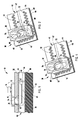
- FIG. 1 is a cross-sectional view of a transceiver device employing a stripline to waveguide transition, according to one embodiment
- FIG. 2 is a perspective view of the stripline to waveguide transition, according to one embodiment
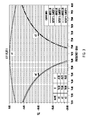
- FIG. 3 is a graph illustrating simulated results achieved with the stripline to waveguide transition shown in FIG. 2 ;
- FIG. 4 is a perspective view of a stripline to waveguide transition, according to another embodiment.
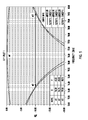
- FIG. 5 is a graph illustrating the simulated results achieved with the stripline to waveguide transition shown in FIG. 4 .
- a cross-sectional view of an RF system 10 comprising a transceiver device or module 12, mounted on an aluminum block 32, coupled through a waveguide 34 in the block 32, followed by a transition 30 to a stripline 40 having stripline feed network 42.
- the stripline 40 and waveguide 34 are arranged substantially perpendicular (ninety degrees) to each other.
- the RF system 10 also includes an antenna or radiator 20.
- the stripline to waveguide transition 30 transitions RF energy between TEM mode propagation in the stripline 40 and TE10 mode propagation in the waveguide 34.
- the RF system 10 may transmit and receive RF energy for use in various systems, such as an automotive radar system, according to one embodiment.
- the transceiver device 12 may include a monolithic millimeter wave integrated circuit (MMIC) 14 mounted onto a low temperature co-fired ceramic (LTCC) substrate 16.
- MMIC 14 may include one or more amplifiers, mixers, and other electrical circuitry.
- the substrate 16 is shown mounted on the conductive block 32 which has the waveguide 34 formed therein.
- the waveguide 34 may be realized in aluminum/copper/FR4 or any other rigid support, according to various embodiments.
- the waveguide 34 is perpendicular to the stripline 40 and its transmission line 42.
- the stripline 40 includes a conductive strip or transmission line 42 separated from first (upper) and second (lower) ground planes 44 and 46 by a dielectric 48 such that line 42 is sandwiched by the dielectric 48.
- RF energy is coupled to the antenna or radiator strip 20 on the antenna dielectric substrate 18 through an aperture 45 in the bottom ground plane 46, according to one embodiment.
- a slot radiator or other radiator may be employed.
- the stripline 40 is a shielded transmission line with conductive strip 42 sandwiched between two dielectric substrates 48, with ground metallization 44 and 46 on either sides of the structure. As there is no need of air-cavity and absorber material, a properly designed stripline 40 offers a cost-effective implementation of the feed network, apart from certain electrical advantages.
- the stripline 40 is connected by its transmission line 42 to a conductive stripline patch 60.
- the stripline to waveguide transition 30 is further illustrated in more detail and is shown absent other components of the RF system 10.
- the waveguide 34 is generally shown as a rectangular hole with rounded corners, with conductive inner walls, often constructed in a block of conductive material, such as aluminum/copper or rigid substrate materials such as FR4 or other dielectric with conductive plated inner walls.
- the waveguide 34 extends from the bottom of the transceiver 12 to a waveguide opening 54 in the upper ground plane 44 of the stripline 40 and is aligned perpendicular to the stripline patch 60.
- the stripline 40 is shown having the conductive transmission line 42 separated from and sandwiched between the first and second ground planes 44 and 46 by the intermediate dielectric 48. As such, the conductive transmission line 42 is electrically isolated from the upper and lower ground planes 44 and 46 which electrically shield the transmission line 42.
- the opening 54 is formed in the upper ground plane 44 of the stripline 40 by etching the metallization in the ground plane 44 to remove an area of the upper ground plane 44 of the stripline 40 to form the opening 54 that generally aligns with the waveguide opening 34.
- the stripline patch 60 is formed of a conductive material fabricated on the dielectric 48 of the stripline 40 and is electrically coupled to the transmission line 42 through an impedance matching transformer 80.
- the transmission line 42 connects to the impedance matching transformer 80 which has a tapered portion and has a predetermined impedance, e.g., 50 ohms.
- the stripline patch 60 may be integrally formed with the transmission line 42.
- the stripline patch 60 is shown in the first embodiment in a generally dog bone shape having substantially parallel opposing sides 62 and 64 and inwardly protruding U-shaped opposing ends 66 and 68. The shape and dimensions of the stripline patch 60 may be optimized for efficient transfer of RF signals in the required signal band.
- the conductive stripline patch 60 is electrically coupled to the conductive strip 42 and is electrically coupled to the overlying waveguide 34 such that the electric field transitions between TEM mode of the stripline 40 and a TE10 mode in the waveguide 34.
- the stripline 40 is further shown having a plurality of plated via holes 52 extending between the top and bottom ground planes 44 and 46 generally located around the outside of the stripline patch 60 and the transmission line 42 so as to form a fence along the stripline 40 that minimizes undesirable parallel plate modes.
- the plurality of via holes 52 may be formed in two roles, generally offset from one another, according to the embodiment shown. According to another embodiment, the plurality of via holes 52 may be formed as a single row. It should be appreciated that the plurality of vias 52 may be provided in various numbers, orientations and shapes may further be provided with a conductive plating to form conductive vias.
- the dielectric 48 may have a thickness and the via hole fence may have a width (edge-to-edge) distance between via hole rows on either side of the stripline 40, as desired to provide proper functioning of the stripline.
- a graph illustrates simulated results of the S-parameters in decibels (dB) versus frequency in gigahertz (GHz) for RF signal transitions achieved with the stripline to waveguide transition 30 shown in FIG. 2 .
- the specific stripline to waveguide transition was designed at a nominal frequency of seventy-six and one-half gigahertz (76.5 GHz), according to one example.
- the stripline to waveguide transition advantageously transitions RF signals between the waveguide and stripline in an efficient manner centered about a frequency of about seventy-six and one-half gigahertz (76.5 GHz).
- a stripline to waveguide transition 30 is illustrated according to another embodiment.
- the conductive stripline patch 60 is shown having a generally oval shape with parallel or slightly rounded opposing sides 72 and 74 and rounded opposing ends 76 and 78, in contrast to the dog bone shape of the first embodiment.
- the conductive stripline patch 60 may be configured having various shapes and sizes which may be optimized for efficient transfer of RF signals in the required operating bandwidth. While dog bone shape and oval shape stripline patches 60 are illustrated in the embodiments shown, it should be appreciated that other sizes and shapes, such as a dumbbell shape patch may be provided, according to other embodiments.
- a graph illustrates simulated results in decibels (dB) versus frequency in gigahertz (GHz) for RF signal transitions achieved with the stripline to waveguide transition 30 shown in FIG. 4 .
- the stripline to waveguide transition 30 provides an efficient transition of RF energy centered about a frequency of seventy-six and one-half gigahertz (76.5 GHz).
- the stripline to waveguide transition 30 advantageously provides for transition or transfer of RF energy from TEM mode of propagation in stripline 40 to the transverse electric propagation of the waveguide 34.
- the stripline to waveguide transition 30 advantageously does not require an expensive air-cavity to be machined into the supporting aluminum block, nor does it require an expensive absorber material. Additionally, the transition 30 may advantageously be effectively integrated within an antenna and transceiver in a single multilayer substrate.
Landscapes
- Waveguide Aerials (AREA)
Applications Claiming Priority (1)
| Application Number | Priority Date | Filing Date | Title |
|---|---|---|---|
| US12/538,931 US20110037530A1 (en) | 2009-08-11 | 2009-08-11 | Stripline to waveguide perpendicular transition |
Publications (1)
| Publication Number | Publication Date |
|---|---|
| EP2290741A1 true EP2290741A1 (de) | 2011-03-02 |
Family
ID=42813111
Family Applications (1)
| Application Number | Title | Priority Date | Filing Date |
|---|---|---|---|
| EP10172035A Withdrawn EP2290741A1 (de) | 2009-08-11 | 2010-08-05 | Perpendikulärer Übergang von einer Streifenleitung zu einem Wellenleiter |
Country Status (2)
| Country | Link |
|---|---|
| US (1) | US20110037530A1 (de) |
| EP (1) | EP2290741A1 (de) |
Cited By (3)
| Publication number | Priority date | Publication date | Assignee | Title |
|---|---|---|---|---|
| WO2013056729A1 (en) * | 2011-10-18 | 2013-04-25 | Telefonaktiebolaget L M Ericsson (Publ) | A microstrip to closed waveguide transition |
| CN111193087A (zh) * | 2018-11-14 | 2020-05-22 | 日本电产株式会社 | 波导装置以及信号发生装置 |
| WO2021094506A1 (en) * | 2019-11-14 | 2021-05-20 | Uhland Goebel | Microwave system and apparatus |
Families Citing this family (12)
| Publication number | Priority date | Publication date | Assignee | Title |
|---|---|---|---|---|
| US8680936B2 (en) | 2011-11-18 | 2014-03-25 | Delphi Technologies, Inc. | Surface mountable microwave signal transition block for microstrip to perpendicular waveguide transition |
| JP5880120B2 (ja) * | 2012-02-20 | 2016-03-08 | 富士通株式会社 | 導波管変換器 |
| JP6515558B2 (ja) * | 2015-02-04 | 2019-05-22 | 富士通株式会社 | 積層型導波路、無線通信モジュール、及び、無線通信システム |
| US10490874B2 (en) * | 2016-03-18 | 2019-11-26 | Te Connectivity Corporation | Board to board contactless interconnect system using waveguide sections connected by conductive gaskets |
| JP6415790B2 (ja) * | 2016-07-05 | 2018-10-31 | 三菱電機株式会社 | 導波管−平面導波路変換器 |
| KR102471197B1 (ko) | 2016-08-25 | 2022-11-28 | 삼성전자 주식회사 | 안테나 장치 및 이를 포함하는 전자 장치 |
| US10957971B2 (en) * | 2019-07-23 | 2021-03-23 | Veoneer Us, Inc. | Feed to waveguide transition structures and related sensor assemblies |
| EP3886244B1 (de) * | 2020-03-26 | 2024-02-21 | Rosemount Tank Radar AB | Mikrowellenübertragungsanordnung, kommunikations- und/oder messsystem und radarfüllstandsmesssystem |
| EP4016620A1 (de) | 2020-12-16 | 2022-06-22 | Nxp B.V. | Package mit einem ic-chip und einem wellenleiter-anreger |
| US11539107B2 (en) | 2020-12-28 | 2022-12-27 | Waymo Llc | Substrate integrated waveguide transition including a metallic layer portion having an open portion that is aligned offset from a centerline |
| CN115207588A (zh) * | 2021-04-09 | 2022-10-18 | 华为技术有限公司 | 一种转接装置、电子设备、终端和转接装置的制备方法 |
| US11978954B2 (en) | 2021-06-02 | 2024-05-07 | The Boeing Company | Compact low-profile aperture antenna with integrated diplexer |
Citations (6)
| Publication number | Priority date | Publication date | Assignee | Title |
|---|---|---|---|---|
| GB865474A (en) * | 1958-08-25 | 1961-04-19 | Cossor Ltd A C | Improvements in and relating to radio frequency coupling devices |
| US4562416A (en) * | 1984-05-31 | 1985-12-31 | Sanders Associates, Inc. | Transition from stripline to waveguide |
| EP0249310A1 (de) * | 1986-06-10 | 1987-12-16 | Canadian Marconi Company | Hohlleiter-Bandleiter-Übergang |
| JPH08139504A (ja) * | 1994-11-14 | 1996-05-31 | Nec Corp | 導波管・平面線路変換器 |
| WO2008114580A1 (ja) * | 2007-03-22 | 2008-09-25 | Hitachi Chemical Co., Ltd. | トリプレート線路-導波管変換器 |
| EP1986265A1 (de) * | 2007-04-27 | 2008-10-29 | Delphi Technologies, Inc. | Wellenleiter für Kopplungsvorrichtungen von Mikrostreifenleitungen |
Family Cites Families (3)
| Publication number | Priority date | Publication date | Assignee | Title |
|---|---|---|---|---|
| US5363464A (en) * | 1993-06-28 | 1994-11-08 | Tangible Domain Inc. | Dielectric/conductive waveguide |
| JP2605654B2 (ja) * | 1995-03-31 | 1997-04-30 | 日本電気株式会社 | 複合マイクロ波回路モジュール及びその製造方法 |
| CN101006610B (zh) * | 2005-03-16 | 2012-04-25 | 日立化成工业株式会社 | 平面天线组件 |
-
2009
- 2009-08-11 US US12/538,931 patent/US20110037530A1/en not_active Abandoned
-
2010
- 2010-08-05 EP EP10172035A patent/EP2290741A1/de not_active Withdrawn
Patent Citations (7)
| Publication number | Priority date | Publication date | Assignee | Title |
|---|---|---|---|---|
| GB865474A (en) * | 1958-08-25 | 1961-04-19 | Cossor Ltd A C | Improvements in and relating to radio frequency coupling devices |
| US4562416A (en) * | 1984-05-31 | 1985-12-31 | Sanders Associates, Inc. | Transition from stripline to waveguide |
| EP0249310A1 (de) * | 1986-06-10 | 1987-12-16 | Canadian Marconi Company | Hohlleiter-Bandleiter-Übergang |
| JPH08139504A (ja) * | 1994-11-14 | 1996-05-31 | Nec Corp | 導波管・平面線路変換器 |
| WO2008114580A1 (ja) * | 2007-03-22 | 2008-09-25 | Hitachi Chemical Co., Ltd. | トリプレート線路-導波管変換器 |
| EP2136433A1 (de) * | 2007-03-22 | 2009-12-23 | Hitachi Chemical Company, Ltd. | Triplate-leitungs-/-wellenleiterumsetzer |
| EP1986265A1 (de) * | 2007-04-27 | 2008-10-29 | Delphi Technologies, Inc. | Wellenleiter für Kopplungsvorrichtungen von Mikrostreifenleitungen |
Non-Patent Citations (1)
| Title |
|---|
| SHIH Y-C ET AL: "Waveguide-to-microstrip transitions for millimeter-wave applications", INTERNATIONAL MICROWAVE SYMPOSIUM. NEW YORK, MAY 25 - 27, 1988; [INTERNATIONAL MICROWAVE SYMPOSIUM], NEW YORK, IEEE, US, 25 May 1988 (1988-05-25), pages 473 - 475, XP010069916 * |
Cited By (5)
| Publication number | Priority date | Publication date | Assignee | Title |
|---|---|---|---|---|
| WO2013056729A1 (en) * | 2011-10-18 | 2013-04-25 | Telefonaktiebolaget L M Ericsson (Publ) | A microstrip to closed waveguide transition |
| US9306264B2 (en) | 2011-10-18 | 2016-04-05 | Telefonaktiebolaget L M Ericsson (Publ) | Transition between a microstrip protruding into an end of a closed waveguide having stepped sidewalls |
| CN111193087A (zh) * | 2018-11-14 | 2020-05-22 | 日本电产株式会社 | 波导装置以及信号发生装置 |
| WO2021094506A1 (en) * | 2019-11-14 | 2021-05-20 | Uhland Goebel | Microwave system and apparatus |
| US12489187B2 (en) | 2019-11-14 | 2025-12-02 | Uhland Goebel | Microwave system and apparatus |
Also Published As
| Publication number | Publication date |
|---|---|
| US20110037530A1 (en) | 2011-02-17 |
Similar Documents
| Publication | Publication Date | Title |
|---|---|---|
| EP2290741A1 (de) | Perpendikulärer Übergang von einer Streifenleitung zu einem Wellenleiter | |
| EP1501152B1 (de) | Signalübergangsvorrichtung für Millimeterwellenbereich | |
| EP3460908B1 (de) | Phasengesteuerte gruppenantenne | |
| US8576023B1 (en) | Stripline-to-waveguide transition including metamaterial layers and an aperture ground plane | |
| US8089327B2 (en) | Waveguide to plural microstrip transition | |
| TWI710163B (zh) | 射頻連接設置 | |
| EP2497146B1 (de) | Verlustarme planare breitband-übertragungsleitung zu wellenleiterübergang | |
| EP1492165B1 (de) | Elektronisches Bauelement-Modul | |
| US8179214B2 (en) | Waveguide connection between a multilayer waveguide substrate and a metal waveguide substrate including a choke structure in the multilayer waveguide | |
| EP2899807A1 (de) | Doppelpolarisierte antenne | |
| EP2945222A1 (de) | Mikrowellen- oder Millimeterwellen-HF-Teil mit Pin-Grid-Array (PGA)- und/oder Ball-Grid-Array (BGA)-Technologien | |
| US11303004B2 (en) | Microstrip-to-waveguide transition including a substrate integrated waveguide with a 90 degree bend section | |
| EP2315304B1 (de) | Streifenleitungsabschlussschaltung mit Resonatoren | |
| EP2600533B1 (de) | Sender-Empfänger-Anordnung | |
| CN109802695A (zh) | 一种信号收发装置以及基站 | |
| JP2002198709A (ja) | 高周波用配線基板 | |
| US10594041B2 (en) | Cavity backed slot antenna with in-cavity resonators | |
| EP3240101B1 (de) | Hochfrequenzverbindung zwischen einer leiterplatte und einem wellenleiter | |
| PL207180B1 (pl) | Przejście między linią mikropaskową a falowodem | |
| KR101496302B1 (ko) | 마이크로스트립 라인과 도파관 사이 밀리미터파 천이 방법 | |
| US8008997B2 (en) | Printed circuit board filter having rows of vias defining a quasi cavity that is below a cutoff frequency | |
| KR101812490B1 (ko) | 기판 집적형 도파관의 표면실장을 위한 전이구조 설계 및 그 제조방법 | |
| US20230088793A1 (en) | Transition structure between transmission line of multilayer pcb and waveguide | |
| CN116325346A (zh) | 射频连接器 | |
| EP1480289A1 (de) | Elektronisches Komponenten-Modul |
Legal Events
| Date | Code | Title | Description |
|---|---|---|---|
| PUAI | Public reference made under article 153(3) epc to a published international application that has entered the european phase |
Free format text: ORIGINAL CODE: 0009012 |
|
| AK | Designated contracting states |
Kind code of ref document: A1 Designated state(s): AL AT BE BG CH CY CZ DE DK EE ES FI FR GB GR HR HU IE IS IT LI LT LU LV MC MK MT NL NO PL PT RO SE SI SK SM TR |
|
| AX | Request for extension of the european patent |
Extension state: BA ME RS |
|
| STAA | Information on the status of an ep patent application or granted ep patent |
Free format text: STATUS: THE APPLICATION IS DEEMED TO BE WITHDRAWN |
|
| 18D | Application deemed to be withdrawn |
Effective date: 20110904 |