EP2290796A2 - Alimentations à découpage et procédés de contrôle associés - Google Patents
Alimentations à découpage et procédés de contrôle associés Download PDFInfo
- Publication number
- EP2290796A2 EP2290796A2 EP10174949A EP10174949A EP2290796A2 EP 2290796 A2 EP2290796 A2 EP 2290796A2 EP 10174949 A EP10174949 A EP 10174949A EP 10174949 A EP10174949 A EP 10174949A EP 2290796 A2 EP2290796 A2 EP 2290796A2
- Authority
- EP
- European Patent Office
- Prior art keywords
- switching
- power supply
- peak current
- signal
- mode power
- Prior art date
- Legal status (The legal status is an assumption and is not a legal conclusion. Google has not performed a legal analysis and makes no representation as to the accuracy of the status listed.)
- Granted
Links
Images


Classifications
-
- H—ELECTRICITY
- H02—GENERATION; CONVERSION OR DISTRIBUTION OF ELECTRIC POWER
- H02M—APPARATUS FOR CONVERSION BETWEEN AC AND AC, BETWEEN AC AND DC, OR BETWEEN DC AND DC, AND FOR USE WITH MAINS OR SIMILAR POWER SUPPLY SYSTEMS; CONVERSION OF DC OR AC INPUT POWER INTO SURGE OUTPUT POWER; CONTROL OR REGULATION THEREOF
- H02M3/00—Conversion of DC power input into DC power output
- H02M3/22—Conversion of DC power input into DC power output with intermediate conversion into AC
- H02M3/24—Conversion of DC power input into DC power output with intermediate conversion into AC by static converters
- H02M3/28—Conversion of DC power input into DC power output with intermediate conversion into AC by static converters using discharge tubes with control electrode or semiconductor devices with control electrode to produce the intermediate AC
- H02M3/325—Conversion of DC power input into DC power output with intermediate conversion into AC by static converters using discharge tubes with control electrode or semiconductor devices with control electrode to produce the intermediate AC using devices of a triode or a transistor type requiring continuous application of a control signal
- H02M3/335—Conversion of DC power input into DC power output with intermediate conversion into AC by static converters using discharge tubes with control electrode or semiconductor devices with control electrode to produce the intermediate AC using devices of a triode or a transistor type requiring continuous application of a control signal using semiconductor devices only
- H02M3/33507—Conversion of DC power input into DC power output with intermediate conversion into AC by static converters using discharge tubes with control electrode or semiconductor devices with control electrode to produce the intermediate AC using devices of a triode or a transistor type requiring continuous application of a control signal using semiconductor devices only with automatic control of the output voltage or current, e.g. flyback converters
- H02M3/33515—Conversion of DC power input into DC power output with intermediate conversion into AC by static converters using discharge tubes with control electrode or semiconductor devices with control electrode to produce the intermediate AC using devices of a triode or a transistor type requiring continuous application of a control signal using semiconductor devices only with automatic control of the output voltage or current, e.g. flyback converters with digital control
-
- H—ELECTRICITY
- H02—GENERATION; CONVERSION OR DISTRIBUTION OF ELECTRIC POWER
- H02M—APPARATUS FOR CONVERSION BETWEEN AC AND AC, BETWEEN AC AND DC, OR BETWEEN DC AND DC, AND FOR USE WITH MAINS OR SIMILAR POWER SUPPLY SYSTEMS; CONVERSION OF DC OR AC INPUT POWER INTO SURGE OUTPUT POWER; CONTROL OR REGULATION THEREOF
- H02M1/00—Details of apparatus for conversion
- H02M1/0003—Details of control, feedback or regulation circuits
- H02M1/0032—Control circuits allowing low power mode operation, e.g. in standby mode
-
- Y—GENERAL TAGGING OF NEW TECHNOLOGICAL DEVELOPMENTS; GENERAL TAGGING OF CROSS-SECTIONAL TECHNOLOGIES SPANNING OVER SEVERAL SECTIONS OF THE IPC; TECHNICAL SUBJECTS COVERED BY FORMER USPC CROSS-REFERENCE ART COLLECTIONS [XRACs] AND DIGESTS
- Y02—TECHNOLOGIES OR APPLICATIONS FOR MITIGATION OR ADAPTATION AGAINST CLIMATE CHANGE
- Y02B—CLIMATE CHANGE MITIGATION TECHNOLOGIES RELATED TO BUILDINGS, e.g. HOUSING, HOUSE APPLIANCES OR RELATED END-USER APPLICATIONS
- Y02B70/00—Technologies for an efficient end-user side electric power management and consumption
- Y02B70/10—Technologies improving the efficiency by using switched-mode power supplies [SMPS], i.e. efficient power electronics conversion e.g. power factor correction or reduction of losses in power supplies or efficient standby modes
Definitions
- the present disclosure relates generally to switching mode power supplies and associated methods of control.
- Switching mode power supplies are used in various applications.
- Multi-mode control is widely adopted in switching mode power supplies because of the generally high conversion efficiency.
- the multi-mode control comprises a pulse skip mode, i.e., the so-called burst mode.
- burst mode the equivalent frequency may become very low, which may generate audible noise if the equivalent frequency is lower than 20kHZ.
- Figure 1 is a schematic diagram of a switching mode power supply in accordance with several embodiments of the technology.
- FIG 2 is a schematic diagram of a controller suitable for use in the switching mode power supply of Figure 1 in accordance with several embodiments of the technology.
- Figure 3 is a graph illustrating an example of multi-mode operation of the controller in Figure 2 .
- Figure 4 shows a waveform of a switching signal used to control the switching circuit when the switching mode power supply in Figure 2 is in burst mode.
- Figure 5 shows an example of a light load peak current processor suitable for use in the controller of Figure 2 .
- FIG. 1 is a schematic diagram of a switching mode power supply 100 in accordance with several embodiments of the technology.
- the switching mode power supply 100 is configured as a flyback converter.
- the switching mode power supply 100 includes a rectifier bridge 101, a transformer 102, a feedback circuit 103, a controller 104, and a current sense resistor (R S ).
- the transformer 102 in one embodiment, includes a primary winding 102-1, a main secondary winding 102-2, and an auxiliary secondary winding 102-3.
- the rectifier bridge 101 receives an AC input signal (V IN ), and converts it into a DC signal received by the primary winding 102-1 of the transformer 102.
- the transformer 102 is controlled by the controller 104 to generate DC output voltages on the secondary windings 102-2, 102-3 of the transformer 102.
- the controller 104 controls the current flow through the primary winding 102-1 of the transformer to effectively switch the transformer 102 on and off.
- the main secondary winding 102-2 provides a DC output voltage (V OUT ) at the output node via a first diode (D 1 ) and an output capacitor (C OUT ).
- the auxiliary secondary winding 102-3 provides a DC voltage source (V CC ) to supply the controller 104 via a second diode (D 2 ), a resistor (R C ) and a capacitor (C 1 ). Also illustrated in Figure 1 is an input capacitor (C IN ) that stores and filters the DC input voltage.
- V CC DC voltage source
- D 2 second diode
- R C resistor
- C 1 capacitor
- C IN input capacitor
- the feedback circuit 103 generates a feedback signal (V FB ) that is inversely proportional to the output voltage (V OUT ) on the main secondary winding 102-2 of the transformer 102.
- the feedback circuit 103 comprises an opto-coupler, a first feedback resistor (R FB1 ), a Zener diode (D 3 ), and a second feedback resistor (R FB2 ).
- the feedback signal is used by the controller 104 to control the switching frequency and the peak current of the switching regulator 100 as a function of the output voltage (V OUT ).
- the opto-coupler includes a photodiode 103-1 and a phototransistor 103-2.
- the intensity of the light emitted by the photodiode 103-1 is inversely proportional to the output voltage (V OUT ).
- the feedback signal (V FB ) is inversely proportional to the output voltage (V OUT ), i.e., it increases as the output voltage (V OUT ) becomes lower and decreases as the output voltage (V OUT ) becomes higher.
- the feedback circuit 103 and controller 104 may be configured such that the feedback signal (V FB ) is proportional to the output voltage (V OUT ) or otherwise varies in relation to the output voltage (V OUT ).
- the controller 104 includes a switching circuit that controls current flow through the primary winding 102-1 of the transformer 102.
- the power supplied to the output node may thus be controlled by varying the frequency at which the switching circuit switches the current through the primary winding 102-1 on and off. This is commonly referred to as the switching frequency of the transformer.
- the controller 104 further includes a frequency control circuit that controls the switching frequency as a function of the feedback signal (V FB ), which is inversely proportional to the output voltage (V OUT ) on the transformer's main secondary winding 102-2.
- the controller 104 includes a current limiting circuit that sets a peak current limit that may be proportional to the output voltage (V OUT ) by causing the switching circuit to suspend current flow through the primary winding 102-1 when the current reaches the peak current limit.
- both the switching frequency and the peak current limit may be regulated based on the output voltage (V OUT ) in order to improve system performance.
- the controller 104 may be configured to cause the switching frequency to decrease as the output voltage (V OUT ) becomes lower, and set the lowest switching frequency when the switching mode power supply enters burst mode.
- the peak current limit may further decrease as the load becomes lighter when the switching mode power supply enters burst mode.
- the controller 104 may be further configured to set the peak current limit proportionally to the output voltage (V OUT ) so that a high efficiency at lighter loads and a high average efficiency is achieved and noises are eliminated in burst mode.
- FIG 2 is a schematic diagram of a controller 200 suitable for use in the switching mode power supply 100 of Figure 1 in accordance with several embodiments of the technology.
- the controller 200 includes a switching circuit 230 (e.g., a MOSFET switch); a frequency control circuit 201, a subtracter 202, a burst mode control circuit 205, a logical circuit 206, a driver 207, a mode transition circuit 209, and a current limiting circuit 208, 210.
- a switching circuit 230 e.g., a MOSFET switch
- the frequency control circuit 201 includes a current source (I S ), an electronic switch (S 1 ), a comparator (U 1 ), a Zener diode (D 4 ), and a resistor (R).
- the frequency control circuit 201 also includes an external capacitor (C 0 ) shown in Figure 1 .
- the electronic switch (S 1 ) is controlled to be on and off by the logical circuit 206. When the electronic switch (S 1 ) is on, the voltage drop across the external capacitor (C 0 ) is reset to zero. When the electronic switch (S 1 ) is off, voltage drop across the external capacitor (C 0 ) increases because of the charge effect of the current source (I S ).
- the comparator (U 1 ) When the voltage drop across the external capacitor (C 0 ) reaches the voltage at the inverting input terminal of the comparator (U 1 ), the comparator (U 1 ) outputs a high level signal to the logical circuit 206, which will provide a logic signal to turn on the electronic switch (S 1 ). Thus the voltage drop across the external capacitor is reset again.
- the burst mode control circuit 205 comprises a hysteresis comparator which receives a voltage reference (V ref ) at one input terminal and receives the output signal (V SUB -V FB ) of the subtracter 202 at the other input terminal.
- the logical circuit 206 comprises a RS flip-flop (U 5 ), which receives the output signal of the frequency control circuit 201 at its set terminal (S), and receives the output signal of the current limiting circuit at its reset terminal (R).
- the logical circuit 206 further comprises an AND gate (U 0 ) which receives the output signal (Q) of the RS flip-flop at its first input terminal, and receives a burst mode signal provided by the burst mode control circuit 205 at its second input terminal.
- U 0 an AND gate which receives the output signal (Q) of the RS flip-flop at its first input terminal, and receives a burst mode signal provided by the burst mode control circuit 205 at its second input terminal.
- the current limiting circuit 208 includes an oscillator (U 2 ) which provides oscillation signals, a pulse processor (U 3 ), and a light load peak current processor (U 4 ).
- the oscillator (U 2 ) provides oscillation signals only when the switching mode power supply enters burst mode.
- the pulse processor (U 3 ) receives the oscillation signals and the logical signal, and provides pulse processed signal (V CL ) based thereupon.
- the light load peak current processor (U 4 ) receives the pulse processed signal (V CL ), and provides a light load peak current processed signal (V th ) based thereupon.
- the current limiting circuit 210 includes a comparator 204, which is coupled to the switch circuit 230 via a leading edge blanking circuit (LEB); a peak current reference judging circuit 203, which receives a voltage reference (V sense ) in one input terminal, and receives the light load peak current processed signal (V th ) or the output signal (V SUB -V FB ) of the subtracter 202 via a status switch (S 2 ) at the other input terminal, and provides a peak current limit (V ir ) based thereupon.
- LEB leading edge blanking circuit
- the LEB circuit is a known circuit that reduces spikes in the signal by introducing a short delay. It should be understood, however, that in other embodiments there could be no LEB circuit.
- the peak current reference judging circuit 203 compares the two input signals and selects the lower one to be its output signal, i.e., the peak current limit (V ir ).
- the mode transition circuit 209 receives the burst mode signal and provides a mode control signal to control the status switch (S 2 ) to be coupled to the output of the light load peak current processor (U 4 ) or to the output of the subtracter.
- the status switch (S 2 ) when the burst mode signal indicates that the switching mode power supply enters burst mode, the status switch (S 2 ) is controlled to be coupled to the output of the light load peak current processor (U 4 ); when the burst mode signal indicates that the switching mode power supply is not under burst mode, the status switch (S 2 ) is controlled to be coupled to the output of the subtracter.
- the switching mode power supply During operation of the switching mode power supply, if the load varies, i.e., the output voltage (V OUT ) varies, the feedback signal (V FB ) varies accordingly which is inversely proportional to the output voltage (V OUT ) as illustrated hereinbefore. As a result, when the load becomes lighter, the switching mode power supply will enter the following modes as depicted in Figure 3 :
- the status switch (S2) is controlled to be coupled to the output of the subtracter 202. Because VSUB-VFB>Vsense, the peak current reference judging circuit 203 selects the voltage reference (Vsense) as the peak current limit (Vir). Thus the peak current limit (Vir) is constant during this mode. On the other hand, the voltage at the inverting input terminal of the comparator (U1) of the frequency control circuit 201 is the feedback signal (VFB).
- the switching frequency (f s ) of the switching mode power supply decreases as the feedback signal (V FB ) increases, i.e., as the load becomes lighter.
- the switching mode power supply is under mode I when the switching frequency varies as a function of the feedback signal and the peak current limit is constant.
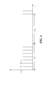
- Figure 4 shows a waveform of the switching signal used to control the switching circuit 230 when the switching mode power supply in Figure 2 is in burst mode.
- the y-axis represents the switching signal
- the x-axis represents time (t).
- Ts is the switching cycle of the switching mode power supply
- X is the switching number when there is switching cycles
- Y is the switching number when there is no switching cycles.
- the embodiments in the technology can at least reduce or prevent the equivalent frequency (f eq ) from dropping into the audible range by further reducing the peak current limit when the switching mode power supply is in burst mode.
- the oscillator (U 2 ) outputs a series of instructions to the pulse processor (U 3 ), so that the pulse processor (U 3 ) starts to sense the switching signals, and record X and Y to get the equivalent frequency (f eq ).
- the pulse processor (U 3 ) further compares X, Y, and the equivalent frequency (f eq ) with preset X set , Y set , and f eqset .
- the pulse processed signal (V CL ) increases; if the equivalent frequency f eq is higher than the preset frequency f eqset , the pulse processed signal (V CL ) decreases.
- the pulse processor (U 3 ) then provides the pulse processed signal (V CL ) to the light load peak current processor (U 4 ), so as to get the light load peak current processed signal (V th ) which varies inversely to the pulse processed signal (V CL ).
- X is regulated to the preset X set
- Y is regulated to the preset Y set
- f eq is regulated to the preset f eqset when the load is rather light.
- the operation of the light load peak current processor (U 4 ) will be described in more detail below.
- Figure 5 depicts an example of a light load peak current processor 300 suitable for use in the controller 200 of Figure 2 .
- the light load peak current processor 300 comprises a first amplifier (A 1 ), a second amplifier (A 2 ), six transistors (Q 1 ⁇ Q 6 ), and three resistors (R 1 ⁇ R 3 ).
- the first transistor (Q 1 ), the second transistor (Q 2 ), the third transistor (Q 3 ), and the fourth transistor (Q 4 ) are p-channel transistors; the fifth transistor (Q 5 ) and the sixth transistor (Q 6 ) are n-channel transistors.
- the non-inverting input terminal of the first amplifier (A1) is coupled to the pulse processed signal (V CL ), the inverting input terminal of the first amplifier (A 1 ) is coupled to the emitter of the fifth transistor (Q 5 ), and the output terminal of the first amplifier (A 1 ) is coupled to the base of the fifth transistor (Q 5 ).
- the first resistor (R 1 ) is coupled between the inverting input terminal of the first amplifier (A 1 ) and ground. That is, the first amplifier (A 1 ), the first resistor (R 1 ), and the fifth transistor (Q 5 ) form a voltage follower.
- the collector of the fifth transistor (Q 5 ) is coupled to the collector of the first transistor (Q 1 ).
- the first transistor (Q 1 ) and the second transistor (Q 2 ) form a first current mirror, wherein the current ratio of the current flow through the first transistor (Q 1 ) and the second transistor (Q 2 ) is 1: m.
- the third transistor (Q 3 ) and the fourth transistor (Q 4 ) form a second current mirror, wherein the current ratio of the current flow through the third transistor (Q 3 ) and the fourth transistor (Q 4 ) is 1: n.
- the second amplifier (A 2 ), the sixth transistor (Q 6 ), and the second resistor (R 2 ) forms a second voltage follower.
- the non-inverting input terminal of the second amplifier (A 2 ) is coupled to a second voltage reference (V R ).
- the collector of the sixth transistor (Q 6 ) is coupled to the collectors of the second transistor (Q 2 ) and the third transistor (Q 3 ).
- the third resistor (R 3 ) is coupled between the collector of the fourth transistor (Q 4 ) and ground.
- the voltage drop across the third resistor (R 3 ) is the output signal of the light load peak current processor 300, i.e., it is the light load peak current processed signal (V th ).
- I 2 m ⁇ I 1
- I 4 n ⁇ I 3
- the light load peak current processed signal (V th ) is inversely proportional to the pulse processed signal (V CL ).
- the pulse processed signal (V CL ) is inversely proportional to the equivalent frequency (f eq ). So the light load peak current processed signal (V th ) is proportional to the equivalent frequency (f eq ). If the equivalent frequency (f eq ) becomes lower, so does the light load peak current processed signal (V th ).
- the light load peak current processed signal (V th ) is lower than the voltage reference (V sense ) at this time. So the peak current reference judging circuit 203 selects the light load peak current processed signal (V th ) as the peak current limit (V ir ). That is, the peak current limit of the switching mode power supply decreases as the load becomes further lighter. In this way, the equivalent frequency (f eq ) increases, which avoids audible noises.
- the status switch (S 2 ) is controlled to be coupled to the output of the subtracter 202 by the mode transition circuit 209. Then the switching mode power supply enters mode I, mode II, or mode III.
Landscapes
- Engineering & Computer Science (AREA)
- Power Engineering (AREA)
- Dc-Dc Converters (AREA)
Applications Claiming Priority (1)
| Application Number | Priority Date | Filing Date | Title |
|---|---|---|---|
| CN2009103064362A CN101645656B (zh) | 2009-09-01 | 2009-09-01 | 电流峰值压缩方法及采用该方法的控制电路 |
Publications (3)
| Publication Number | Publication Date |
|---|---|
| EP2290796A2 true EP2290796A2 (fr) | 2011-03-02 |
| EP2290796A3 EP2290796A3 (fr) | 2013-11-20 |
| EP2290796B1 EP2290796B1 (fr) | 2016-11-09 |
Family
ID=41657396
Family Applications (1)
| Application Number | Title | Priority Date | Filing Date |
|---|---|---|---|
| EP10174949.7A Active EP2290796B1 (fr) | 2009-09-01 | 2010-09-01 | Convertisseur à découpage et un mode rafale |
Country Status (3)
| Country | Link |
|---|---|
| US (1) | US8391030B2 (fr) |
| EP (1) | EP2290796B1 (fr) |
| CN (1) | CN101645656B (fr) |
Families Citing this family (17)
| Publication number | Priority date | Publication date | Assignee | Title |
|---|---|---|---|---|
| US9735673B2 (en) * | 2011-03-30 | 2017-08-15 | Infineon Technologies Ag | Burst-mode operation of a switching converter |
| CN102201738B (zh) * | 2011-05-18 | 2014-12-31 | 上海新进半导体制造有限公司 | 一种电源转换器的噪音控制电路和方法 |
| CN102664525B (zh) | 2012-05-08 | 2014-08-27 | 成都芯源系统有限公司 | 一种开关电源电路 |
| ITMI20121231A1 (it) * | 2012-07-16 | 2014-01-17 | St Microelectronics Srl | Metodo di controllo burst-mode per basso consumo in ingresso in convertitori risonanti e relativo dispositivo di controllo |
| CN102801305B (zh) * | 2012-08-14 | 2015-07-08 | 成都芯源系统有限公司 | 峰值电流信号产生电路,开关电源电路及其方法 |
| EP2731247B1 (fr) * | 2012-11-13 | 2021-03-17 | Delta Electronics, Inc. | Procédé pour convertisseur indirect |
| CN103219900B (zh) * | 2013-04-17 | 2016-08-10 | 上海新进半导体制造有限公司 | 一种消除pfm开关电源噪声的电路、方法及开关电源 |
| CN104348357B (zh) * | 2013-07-31 | 2018-02-09 | 通嘉科技股份有限公司 | 用以降低电源转换器的触碰电流的控制电路及其操作方法 |
| CN103532352B (zh) * | 2013-10-25 | 2016-01-06 | 上海灿矽半导体科技有限公司 | 用于消除开关电源轻载音频噪声的控制电路和控制方法 |
| US9680383B2 (en) * | 2014-11-07 | 2017-06-13 | Power Integrations, Inc. | Input overvoltage protection using current limit |
| US9450478B1 (en) * | 2015-04-10 | 2016-09-20 | Power Integrations, Inc. | Load responsive jitter |
| US9742265B2 (en) * | 2015-06-17 | 2017-08-22 | Chicony Power Technology Co., Ltd. | Power supply method for avoiding audio noise and power supply apparatus for avoiding audio noise |
| CN105553263B (zh) * | 2015-12-28 | 2018-04-06 | 成都芯源系统有限公司 | 恒定导通时长控制的开关电源及其控制电路和控制方法 |
| US10205394B2 (en) * | 2016-09-16 | 2019-02-12 | Power Integrations, Inc. | Switched mode power converter controller with ramp time modulation with jitter frequency |
| CN110247554B (zh) * | 2018-03-09 | 2020-09-11 | 台达电子工业股份有限公司 | 变换装置与其控制方法 |
| US10250118B1 (en) * | 2018-04-16 | 2019-04-02 | Nxp B.V. | PWM mode boost switching regulator with programmable pulse skip mode |
| CN110518800B (zh) * | 2018-05-21 | 2020-06-12 | 台达电子工业股份有限公司 | 一种反激变换器及其控制方法 |
Family Cites Families (9)
| Publication number | Priority date | Publication date | Assignee | Title |
|---|---|---|---|---|
| KR100379057B1 (ko) * | 1999-04-10 | 2003-04-08 | 페어차일드코리아반도체 주식회사 | 버스트 모드 스위칭 모드 파워 서플라이 |
| US7211991B2 (en) * | 2000-08-08 | 2007-05-01 | Power Integrations, Inc. | Method and apparatus for reducing audio noise in a switching regulator |
| US6525514B1 (en) * | 2000-08-08 | 2003-02-25 | Power Integrations, Inc. | Method and apparatus for reducing audio noise in a switching regulator |
| CN1855680B (zh) * | 2005-04-26 | 2011-05-25 | 美国芯源系统股份有限公司 | 开关电源的控制方法及采用该控制方法的产品 |
| CN101167236B (zh) * | 2005-07-15 | 2010-08-25 | 半导体元件工业有限责任公司 | 电源控制器及其方法 |
| US7233504B2 (en) * | 2005-08-26 | 2007-06-19 | Power Integration, Inc. | Method and apparatus for digital control of a switching regulator |
| US7911808B2 (en) * | 2007-02-10 | 2011-03-22 | Active-Semi, Inc. | Primary side constant output current controller with highly improved accuracy |
| US7983061B2 (en) * | 2008-02-22 | 2011-07-19 | System General Corporation | Switching controller capable of reducing acoustic noise for power converters |
| CN101425753B (zh) * | 2008-12-22 | 2010-08-04 | 深圳市明微电子股份有限公司 | 一种开关电源线电压补偿方法及自适应采样器 |
-
2009
- 2009-09-01 CN CN2009103064362A patent/CN101645656B/zh active Active
-
2010
- 2010-08-31 US US12/873,103 patent/US8391030B2/en active Active
- 2010-09-01 EP EP10174949.7A patent/EP2290796B1/fr active Active
Non-Patent Citations (1)
| Title |
|---|
| None |
Also Published As
| Publication number | Publication date |
|---|---|
| US20110051470A1 (en) | 2011-03-03 |
| EP2290796A3 (fr) | 2013-11-20 |
| CN101645656A (zh) | 2010-02-10 |
| EP2290796B1 (fr) | 2016-11-09 |
| CN101645656B (zh) | 2011-09-14 |
| US8391030B2 (en) | 2013-03-05 |
Similar Documents
| Publication | Publication Date | Title |
|---|---|---|
| EP2290796A2 (fr) | Alimentations à découpage et procédés de contrôle associés | |
| US8824173B2 (en) | Systems and methods for constant voltage control and constant current control | |
| US10291131B2 (en) | Systems and methods for peak current adjustments in power conversion systems | |
| KR100856900B1 (ko) | 버스트 모드 스위칭 모드 파워 서플라이 | |
| US10483856B2 (en) | Systems and methods with prediction mechanisms for synchronization rectifier controllers | |
| CN101286701B (zh) | 开关电源 | |
| US20180109195A1 (en) | Systems and methods for voltage control and current control of power conversion systems with multiple operation modes | |
| US20180013352A1 (en) | Systems and methods for regulating power conversion systems with output detection and synchronized rectifying mechanisms | |
| JP5532135B2 (ja) | スイッチング制御回路及びスイッチング電源装置 | |
| US20090201705A1 (en) | Energy converting apparatus, and semiconductor device and switching control method used therein | |
| US10630187B2 (en) | Switching power supply device and semiconductor device | |
| US9847711B2 (en) | Switching power supply device control circuit and switching power supply device | |
| JP2005117814A (ja) | スイッチング電源装置 | |
| JP2009153364A (ja) | スイッチング電源装置 | |
| JP2017127109A (ja) | スイッチング電源装置 | |
| CN112134461B (zh) | 用于多输出电压功率转换器的多模式控制 | |
| US10135347B2 (en) | Switching power supply device | |
| JP7707843B2 (ja) | 電源回路 | |
| US12431810B2 (en) | Isolated switching converter for peak power demand and control method thereof | |
| CN110768533A (zh) | 电源控制器与相关的控制方法 | |
| US20110149612A1 (en) | Control Method and Controller with constant output current control | |
| JP2006158042A (ja) | スイッチング電源装置 | |
| WO2010125751A1 (fr) | Dispositif de commutation d'alimentation électrique | |
| JP7400188B2 (ja) | 制御装置 | |
| JP2003033017A (ja) | スイッチング電源装置 |
Legal Events
| Date | Code | Title | Description |
|---|---|---|---|
| PUAI | Public reference made under article 153(3) epc to a published international application that has entered the european phase |
Free format text: ORIGINAL CODE: 0009012 |
|
| AK | Designated contracting states |
Kind code of ref document: A2 Designated state(s): AL AT BE BG CH CY CZ DE DK EE ES FI FR GB GR HR HU IE IS IT LI LT LU LV MC MK MT NL NO PL PT RO SE SI SK SM TR |
|
| AX | Request for extension of the european patent |
Extension state: BA ME RS |
|
| PUAL | Search report despatched |
Free format text: ORIGINAL CODE: 0009013 |
|
| AK | Designated contracting states |
Kind code of ref document: A3 Designated state(s): AL AT BE BG CH CY CZ DE DK EE ES FI FR GB GR HR HU IE IS IT LI LT LU LV MC MK MT NL NO PL PT RO SE SI SK SM TR |
|
| AX | Request for extension of the european patent |
Extension state: BA ME RS |
|
| RIC1 | Information provided on ipc code assigned before grant |
Ipc: H02M 3/335 20060101AFI20131016BHEP |
|
| 17P | Request for examination filed |
Effective date: 20140515 |
|
| 17Q | First examination report despatched |
Effective date: 20150302 |
|
| RAP1 | Party data changed (applicant data changed or rights of an application transferred) |
Owner name: MONOLITHIC POWER SYSTEMS, INC. |
|
| GRAP | Despatch of communication of intention to grant a patent |
Free format text: ORIGINAL CODE: EPIDOSNIGR1 |
|
| INTG | Intention to grant announced |
Effective date: 20160520 |
|
| GRAS | Grant fee paid |
Free format text: ORIGINAL CODE: EPIDOSNIGR3 |
|
| GRAA | (expected) grant |
Free format text: ORIGINAL CODE: 0009210 |
|
| AK | Designated contracting states |
Kind code of ref document: B1 Designated state(s): AL AT BE BG CH CY CZ DE DK EE ES FI FR GB GR HR HU IE IS IT LI LT LU LV MC MK MT NL NO PL PT RO SE SI SK SM TR |
|
| REG | Reference to a national code |
Ref country code: GB Ref legal event code: FG4D |
|
| REG | Reference to a national code |
Ref country code: AT Ref legal event code: REF Ref document number: 844729 Country of ref document: AT Kind code of ref document: T Effective date: 20161115 Ref country code: CH Ref legal event code: EP |
|
| REG | Reference to a national code |
Ref country code: IE Ref legal event code: FG4D |
|
| REG | Reference to a national code |
Ref country code: DE Ref legal event code: R096 Ref document number: 602010037786 Country of ref document: DE |
|
| PG25 | Lapsed in a contracting state [announced via postgrant information from national office to epo] |
Ref country code: LV Free format text: LAPSE BECAUSE OF FAILURE TO SUBMIT A TRANSLATION OF THE DESCRIPTION OR TO PAY THE FEE WITHIN THE PRESCRIBED TIME-LIMIT Effective date: 20161109 |
|
| REG | Reference to a national code |
Ref country code: LT Ref legal event code: MG4D |
|
| REG | Reference to a national code |
Ref country code: NL Ref legal event code: MP Effective date: 20161109 |
|
| REG | Reference to a national code |
Ref country code: AT Ref legal event code: MK05 Ref document number: 844729 Country of ref document: AT Kind code of ref document: T Effective date: 20161109 |
|
| PG25 | Lapsed in a contracting state [announced via postgrant information from national office to epo] |
Ref country code: LT Free format text: LAPSE BECAUSE OF FAILURE TO SUBMIT A TRANSLATION OF THE DESCRIPTION OR TO PAY THE FEE WITHIN THE PRESCRIBED TIME-LIMIT Effective date: 20161109 Ref country code: NL Free format text: LAPSE BECAUSE OF FAILURE TO SUBMIT A TRANSLATION OF THE DESCRIPTION OR TO PAY THE FEE WITHIN THE PRESCRIBED TIME-LIMIT Effective date: 20161109 Ref country code: SE Free format text: LAPSE BECAUSE OF FAILURE TO SUBMIT A TRANSLATION OF THE DESCRIPTION OR TO PAY THE FEE WITHIN THE PRESCRIBED TIME-LIMIT Effective date: 20161109 Ref country code: GR Free format text: LAPSE BECAUSE OF FAILURE TO SUBMIT A TRANSLATION OF THE DESCRIPTION OR TO PAY THE FEE WITHIN THE PRESCRIBED TIME-LIMIT Effective date: 20170210 Ref country code: NO Free format text: LAPSE BECAUSE OF FAILURE TO SUBMIT A TRANSLATION OF THE DESCRIPTION OR TO PAY THE FEE WITHIN THE PRESCRIBED TIME-LIMIT Effective date: 20170209 |
|
| PG25 | Lapsed in a contracting state [announced via postgrant information from national office to epo] |
Ref country code: ES Free format text: LAPSE BECAUSE OF FAILURE TO SUBMIT A TRANSLATION OF THE DESCRIPTION OR TO PAY THE FEE WITHIN THE PRESCRIBED TIME-LIMIT Effective date: 20161109 Ref country code: AT Free format text: LAPSE BECAUSE OF FAILURE TO SUBMIT A TRANSLATION OF THE DESCRIPTION OR TO PAY THE FEE WITHIN THE PRESCRIBED TIME-LIMIT Effective date: 20161109 Ref country code: PL Free format text: LAPSE BECAUSE OF FAILURE TO SUBMIT A TRANSLATION OF THE DESCRIPTION OR TO PAY THE FEE WITHIN THE PRESCRIBED TIME-LIMIT Effective date: 20161109 Ref country code: FI Free format text: LAPSE BECAUSE OF FAILURE TO SUBMIT A TRANSLATION OF THE DESCRIPTION OR TO PAY THE FEE WITHIN THE PRESCRIBED TIME-LIMIT Effective date: 20161109 Ref country code: PT Free format text: LAPSE BECAUSE OF FAILURE TO SUBMIT A TRANSLATION OF THE DESCRIPTION OR TO PAY THE FEE WITHIN THE PRESCRIBED TIME-LIMIT Effective date: 20170309 Ref country code: IS Free format text: LAPSE BECAUSE OF FAILURE TO SUBMIT A TRANSLATION OF THE DESCRIPTION OR TO PAY THE FEE WITHIN THE PRESCRIBED TIME-LIMIT Effective date: 20170309 Ref country code: HR Free format text: LAPSE BECAUSE OF FAILURE TO SUBMIT A TRANSLATION OF THE DESCRIPTION OR TO PAY THE FEE WITHIN THE PRESCRIBED TIME-LIMIT Effective date: 20161109 |
|
| PG25 | Lapsed in a contracting state [announced via postgrant information from national office to epo] |
Ref country code: SK Free format text: LAPSE BECAUSE OF FAILURE TO SUBMIT A TRANSLATION OF THE DESCRIPTION OR TO PAY THE FEE WITHIN THE PRESCRIBED TIME-LIMIT Effective date: 20161109 Ref country code: EE Free format text: LAPSE BECAUSE OF FAILURE TO SUBMIT A TRANSLATION OF THE DESCRIPTION OR TO PAY THE FEE WITHIN THE PRESCRIBED TIME-LIMIT Effective date: 20161109 Ref country code: CZ Free format text: LAPSE BECAUSE OF FAILURE TO SUBMIT A TRANSLATION OF THE DESCRIPTION OR TO PAY THE FEE WITHIN THE PRESCRIBED TIME-LIMIT Effective date: 20161109 Ref country code: RO Free format text: LAPSE BECAUSE OF FAILURE TO SUBMIT A TRANSLATION OF THE DESCRIPTION OR TO PAY THE FEE WITHIN THE PRESCRIBED TIME-LIMIT Effective date: 20161109 Ref country code: DK Free format text: LAPSE BECAUSE OF FAILURE TO SUBMIT A TRANSLATION OF THE DESCRIPTION OR TO PAY THE FEE WITHIN THE PRESCRIBED TIME-LIMIT Effective date: 20161109 |
|
| REG | Reference to a national code |
Ref country code: DE Ref legal event code: R097 Ref document number: 602010037786 Country of ref document: DE |
|
| PG25 | Lapsed in a contracting state [announced via postgrant information from national office to epo] |
Ref country code: BG Free format text: LAPSE BECAUSE OF FAILURE TO SUBMIT A TRANSLATION OF THE DESCRIPTION OR TO PAY THE FEE WITHIN THE PRESCRIBED TIME-LIMIT Effective date: 20170209 Ref country code: BE Free format text: LAPSE BECAUSE OF FAILURE TO SUBMIT A TRANSLATION OF THE DESCRIPTION OR TO PAY THE FEE WITHIN THE PRESCRIBED TIME-LIMIT Effective date: 20161109 Ref country code: IT Free format text: LAPSE BECAUSE OF FAILURE TO SUBMIT A TRANSLATION OF THE DESCRIPTION OR TO PAY THE FEE WITHIN THE PRESCRIBED TIME-LIMIT Effective date: 20161109 Ref country code: SM Free format text: LAPSE BECAUSE OF FAILURE TO SUBMIT A TRANSLATION OF THE DESCRIPTION OR TO PAY THE FEE WITHIN THE PRESCRIBED TIME-LIMIT Effective date: 20161109 |
|
| PLBE | No opposition filed within time limit |
Free format text: ORIGINAL CODE: 0009261 |
|
| STAA | Information on the status of an ep patent application or granted ep patent |
Free format text: STATUS: NO OPPOSITION FILED WITHIN TIME LIMIT |
|
| 26N | No opposition filed |
Effective date: 20170810 |
|
| PG25 | Lapsed in a contracting state [announced via postgrant information from national office to epo] |
Ref country code: SI Free format text: LAPSE BECAUSE OF FAILURE TO SUBMIT A TRANSLATION OF THE DESCRIPTION OR TO PAY THE FEE WITHIN THE PRESCRIBED TIME-LIMIT Effective date: 20161109 |
|
| REG | Reference to a national code |
Ref country code: CH Ref legal event code: PL |
|
| GBPC | Gb: european patent ceased through non-payment of renewal fee |
Effective date: 20170901 |
|
| PG25 | Lapsed in a contracting state [announced via postgrant information from national office to epo] |
Ref country code: MC Free format text: LAPSE BECAUSE OF FAILURE TO SUBMIT A TRANSLATION OF THE DESCRIPTION OR TO PAY THE FEE WITHIN THE PRESCRIBED TIME-LIMIT Effective date: 20161109 |
|
| REG | Reference to a national code |
Ref country code: IE Ref legal event code: MM4A |
|
| PG25 | Lapsed in a contracting state [announced via postgrant information from national office to epo] |
Ref country code: LU Free format text: LAPSE BECAUSE OF NON-PAYMENT OF DUE FEES Effective date: 20170901 |
|
| REG | Reference to a national code |
Ref country code: FR Ref legal event code: ST Effective date: 20180531 |
|
| PG25 | Lapsed in a contracting state [announced via postgrant information from national office to epo] |
Ref country code: LI Free format text: LAPSE BECAUSE OF NON-PAYMENT OF DUE FEES Effective date: 20170930 Ref country code: CH Free format text: LAPSE BECAUSE OF NON-PAYMENT OF DUE FEES Effective date: 20170930 Ref country code: IE Free format text: LAPSE BECAUSE OF NON-PAYMENT OF DUE FEES Effective date: 20170901 Ref country code: GB Free format text: LAPSE BECAUSE OF NON-PAYMENT OF DUE FEES Effective date: 20170901 |
|
| PG25 | Lapsed in a contracting state [announced via postgrant information from national office to epo] |
Ref country code: FR Free format text: LAPSE BECAUSE OF NON-PAYMENT OF DUE FEES Effective date: 20171002 |
|
| PG25 | Lapsed in a contracting state [announced via postgrant information from national office to epo] |
Ref country code: MT Free format text: LAPSE BECAUSE OF NON-PAYMENT OF DUE FEES Effective date: 20170901 |
|
| PG25 | Lapsed in a contracting state [announced via postgrant information from national office to epo] |
Ref country code: HU Free format text: LAPSE BECAUSE OF FAILURE TO SUBMIT A TRANSLATION OF THE DESCRIPTION OR TO PAY THE FEE WITHIN THE PRESCRIBED TIME-LIMIT; INVALID AB INITIO Effective date: 20100901 |
|
| PG25 | Lapsed in a contracting state [announced via postgrant information from national office to epo] |
Ref country code: CY Free format text: LAPSE BECAUSE OF NON-PAYMENT OF DUE FEES Effective date: 20161109 |
|
| PG25 | Lapsed in a contracting state [announced via postgrant information from national office to epo] |
Ref country code: MK Free format text: LAPSE BECAUSE OF FAILURE TO SUBMIT A TRANSLATION OF THE DESCRIPTION OR TO PAY THE FEE WITHIN THE PRESCRIBED TIME-LIMIT Effective date: 20161109 |
|
| PG25 | Lapsed in a contracting state [announced via postgrant information from national office to epo] |
Ref country code: TR Free format text: LAPSE BECAUSE OF FAILURE TO SUBMIT A TRANSLATION OF THE DESCRIPTION OR TO PAY THE FEE WITHIN THE PRESCRIBED TIME-LIMIT Effective date: 20161109 |
|
| PG25 | Lapsed in a contracting state [announced via postgrant information from national office to epo] |
Ref country code: AL Free format text: LAPSE BECAUSE OF FAILURE TO SUBMIT A TRANSLATION OF THE DESCRIPTION OR TO PAY THE FEE WITHIN THE PRESCRIBED TIME-LIMIT Effective date: 20161109 |
|
| PGFP | Annual fee paid to national office [announced via postgrant information from national office to epo] |
Ref country code: DE Payment date: 20250929 Year of fee payment: 16 |