EP2291712B1 - Monocristaux volumineux de polyène phénolique à configuration figée, couches minces cristallines et guides d'ondes optiques destinés à des applications électro-optiques et d'ondes thz - Google Patents
Monocristaux volumineux de polyène phénolique à configuration figée, couches minces cristallines et guides d'ondes optiques destinés à des applications électro-optiques et d'ondes thz Download PDFInfo
- Publication number
- EP2291712B1 EP2291712B1 EP09741647.3A EP09741647A EP2291712B1 EP 2291712 B1 EP2291712 B1 EP 2291712B1 EP 09741647 A EP09741647 A EP 09741647A EP 2291712 B1 EP2291712 B1 EP 2291712B1
- Authority
- EP
- European Patent Office
- Prior art keywords
- substrate
- crystals
- single crystal
- electro
- optical
- Prior art date
- Legal status (The legal status is an assumption and is not a legal conclusion. Google has not performed a legal analysis and makes no representation as to the accuracy of the status listed.)
- Active
Links
Images




Classifications
-
- G—PHYSICS
- G02—OPTICS
- G02F—OPTICAL DEVICES OR ARRANGEMENTS FOR THE CONTROL OF LIGHT BY MODIFICATION OF THE OPTICAL PROPERTIES OF THE MEDIA OF THE ELEMENTS INVOLVED THEREIN; NON-LINEAR OPTICS; FREQUENCY-CHANGING OF LIGHT; OPTICAL LOGIC ELEMENTS; OPTICAL ANALOGUE/DIGITAL CONVERTERS
- G02F1/00—Devices or arrangements for the control of the intensity, colour, phase, polarisation or direction of light arriving from an independent light source, e.g. switching, gating or modulating; Non-linear optics
- G02F1/35—Non-linear optics
- G02F1/355—Non-linear optics characterised by the materials used
- G02F1/361—Organic materials
- G02F1/3611—Organic materials containing Nitrogen
-
- G—PHYSICS
- G02—OPTICS
- G02F—OPTICAL DEVICES OR ARRANGEMENTS FOR THE CONTROL OF LIGHT BY MODIFICATION OF THE OPTICAL PROPERTIES OF THE MEDIA OF THE ELEMENTS INVOLVED THEREIN; NON-LINEAR OPTICS; FREQUENCY-CHANGING OF LIGHT; OPTICAL LOGIC ELEMENTS; OPTICAL ANALOGUE/DIGITAL CONVERTERS
- G02F1/00—Devices or arrangements for the control of the intensity, colour, phase, polarisation or direction of light arriving from an independent light source, e.g. switching, gating or modulating; Non-linear optics
- G02F1/01—Devices or arrangements for the control of the intensity, colour, phase, polarisation or direction of light arriving from an independent light source, e.g. switching, gating or modulating; Non-linear optics for the control of the intensity, phase, polarisation or colour
- G02F1/061—Devices or arrangements for the control of the intensity, colour, phase, polarisation or direction of light arriving from an independent light source, e.g. switching, gating or modulating; Non-linear optics for the control of the intensity, phase, polarisation or colour based on electro-optical organic material
-
- G—PHYSICS
- G02—OPTICS
- G02F—OPTICAL DEVICES OR ARRANGEMENTS FOR THE CONTROL OF LIGHT BY MODIFICATION OF THE OPTICAL PROPERTIES OF THE MEDIA OF THE ELEMENTS INVOLVED THEREIN; NON-LINEAR OPTICS; FREQUENCY-CHANGING OF LIGHT; OPTICAL LOGIC ELEMENTS; OPTICAL ANALOGUE/DIGITAL CONVERTERS
- G02F1/00—Devices or arrangements for the control of the intensity, colour, phase, polarisation or direction of light arriving from an independent light source, e.g. switching, gating or modulating; Non-linear optics
- G02F1/01—Devices or arrangements for the control of the intensity, colour, phase, polarisation or direction of light arriving from an independent light source, e.g. switching, gating or modulating; Non-linear optics for the control of the intensity, phase, polarisation or colour
- G02F1/061—Devices or arrangements for the control of the intensity, colour, phase, polarisation or direction of light arriving from an independent light source, e.g. switching, gating or modulating; Non-linear optics for the control of the intensity, phase, polarisation or colour based on electro-optical organic material
- G02F1/065—Devices or arrangements for the control of the intensity, colour, phase, polarisation or direction of light arriving from an independent light source, e.g. switching, gating or modulating; Non-linear optics for the control of the intensity, phase, polarisation or colour based on electro-optical organic material in an optical waveguide structure
-
- G—PHYSICS
- G02—OPTICS
- G02F—OPTICAL DEVICES OR ARRANGEMENTS FOR THE CONTROL OF LIGHT BY MODIFICATION OF THE OPTICAL PROPERTIES OF THE MEDIA OF THE ELEMENTS INVOLVED THEREIN; NON-LINEAR OPTICS; FREQUENCY-CHANGING OF LIGHT; OPTICAL LOGIC ELEMENTS; OPTICAL ANALOGUE/DIGITAL CONVERTERS
- G02F1/00—Devices or arrangements for the control of the intensity, colour, phase, polarisation or direction of light arriving from an independent light source, e.g. switching, gating or modulating; Non-linear optics
- G02F1/01—Devices or arrangements for the control of the intensity, colour, phase, polarisation or direction of light arriving from an independent light source, e.g. switching, gating or modulating; Non-linear optics for the control of the intensity, phase, polarisation or colour
- G02F1/21—Devices or arrangements for the control of the intensity, colour, phase, polarisation or direction of light arriving from an independent light source, e.g. switching, gating or modulating; Non-linear optics for the control of the intensity, phase, polarisation or colour by interference
- G02F1/225—Devices or arrangements for the control of the intensity, colour, phase, polarisation or direction of light arriving from an independent light source, e.g. switching, gating or modulating; Non-linear optics for the control of the intensity, phase, polarisation or colour by interference in an optical waveguide structure
-
- G—PHYSICS
- G02—OPTICS
- G02F—OPTICAL DEVICES OR ARRANGEMENTS FOR THE CONTROL OF LIGHT BY MODIFICATION OF THE OPTICAL PROPERTIES OF THE MEDIA OF THE ELEMENTS INVOLVED THEREIN; NON-LINEAR OPTICS; FREQUENCY-CHANGING OF LIGHT; OPTICAL LOGIC ELEMENTS; OPTICAL ANALOGUE/DIGITAL CONVERTERS
- G02F2203/00—Function characteristic
- G02F2203/13—Function characteristic involving THZ radiation
-
- G—PHYSICS
- G02—OPTICS
- G02F—OPTICAL DEVICES OR ARRANGEMENTS FOR THE CONTROL OF LIGHT BY MODIFICATION OF THE OPTICAL PROPERTIES OF THE MEDIA OF THE ELEMENTS INVOLVED THEREIN; NON-LINEAR OPTICS; FREQUENCY-CHANGING OF LIGHT; OPTICAL LOGIC ELEMENTS; OPTICAL ANALOGUE/DIGITAL CONVERTERS
- G02F2203/00—Function characteristic
- G02F2203/15—Function characteristic involving resonance effects, e.g. resonantly enhanced interaction
Definitions
- the invention concerns Phenolic Configurationally Locked Polyene compounds, which are, in crystalline form, especially suited as highly efficient nonlinear optical organic material.
- the invention also concerns methods for growth of crystalline thin films or bulk crystals.
- the compounds are suited and the methods may be used for manufacturing optical elements for several bulk and integrated optical applications, e.g. for electro-Optics and THz-Wave applications.
- nonlinear optical organic materials are of great interest for various applications in optical telecommunication [1, 2, 3, 4] and terahertz wave applications [5, 6, 7]. Due to their almost purely electronic response, organic materials show extremely fast optical nonlinearities compared to their inorganic counterparts, and therefore promise to meet future requirements for ultra-high bandwidth photonic devices (up to 200 GHz an more) for next-generation fiber-optical data transmission networks (ultrafast internet), local-area networks and on-chip applications, as well as sensor applications and field detection.
- a highly asymmetric electronic response of the material to the external electric field is required.
- a noncentrosymmetric arrangement of the molecules may be induced by spontaneous self-assembly by intermolecular interactions in the crystalline lattice or external poling in a polymer matrix.
- chromophore density and photochemical stability [8] are significantly superior to those of polymers.
- the state-of-the-art organic nonlinear optical crystals are ionic stilbazolium salts with large electro-optic coefficients of more than 50 pm/V at 1.3 and 1.55 ⁇ m, such as DAST (4'-dimethylamino- N -methyl-4-stilbazolium tosylate) [11] and DSTMS (4'-dimethylamino- N -methyl-4-stilbazolium 2,4,6-trimethylbenzenesulfonate) [7].
- their thermal stability is insufficient for applying melt-based crystal growth techniques, which considerably limits the applicability of these crystals for very large scale integrated photonic structures.
- they have a tendency to form a centrosymmetric hydrated phase in presence of water. Therefore, there is a strong interest to develop new highly nonlinear optical organic crystals with a possibility of melt-based material processing.
- CLP configurationally locked polyene
- the invention is based on the development of non-ionic organic configurationally locked polyene (CLP) single crystals containing a phenolic electron donor with very large electro-optic response and high thermal and environmental stability.
- CLP non-ionic organic configurationally locked polyene
- R1 and R2 being identical or different, are independently chosen from the group consisting of: H (Hydrogen), D (Deutrium), any perhalogenated, halogenated or non-halogenated aliphatic or aromatic group, wherein at least one carbon atom of this aliphatic or aromatic group is optionally functionalized with at least one of: hydroxy, ether, ester, amino, silyl, and siloxy group.
- Phenolic CLP crystals OH1 with orthorhombic space group Pna2 1 (point group mm2) exhibit large second-order nonlinear optical figures of merit, high thermal stability and very favorable crystal growth characteristics. Higher solubility in methanol and a larger temperature difference between the melting temperature and the decomposition temperature of OH1 compared to analogous CLP crystals, are of advantage for solution and melt crystal growth, respectively.
- Acentric bulk OH1 crystals of large sizes with side lengths of more than 1 cm with excellent optical quality have been successfully grown from methanol solution.
- the OH1 crystals exhibit a large macroscopic nonlinearity with four times larger powder second harmonic generation efficiency than that of analogous CLP crystals containing dimethyl amino electron donor.
- a very high potential of OH1 crystals for broadband THz wave emitters in the full frequency range of 0.1-3 THz by optical rectification of 160 fs pulses has been demonstrated.
- OH1 exhibits excellent nonlinear optical and electro-optical properties.
- OH1 shows a large birefringence of ⁇ n >0.55 and a low absorption of ⁇ 1 cm -1 in a large wavelength range between 800 and 1400 nm.
- the electro-optic coefficients r 333 , r 223 and r 113 have been measured at the wavelengths of 633, 785, 1064, and 1319 nm.
- Phenolic CLP crystals OH3 without a methyl group on the cyclohexene ring exhibit an isomorphic structure to OH2 crystals with ⁇ p ⁇ 13°.
- the method according to the invention for growing a thin single crystal film of OH1 comprises the following steps: providing the compound in a liquid state, in particular in solution or in melt; providing the substrate; growing crystals on at least one surface of the substrate.
- the substrate for example a Silicon, Silicate glass (SiO 2 ), Borosilicate glass, polymer substrate, is functionalized at at least one surface, by -OH, or -CNgroups. This may for example be achieved by treating the surface by solutions, e.g. with Piranha solution (mixture of H 2 SO 4 and H 2 O 2 ), or by silanization.
- Piranha solution mixture of H 2 SO 4 and H 2 O 2
- silanization silanization
- the substrate may be unstructured (planar, homogenous material), for example a standard glass slide or Silicon wafer. It may also be a prefabricated substrate that comprises a surface structured with at least one recesses, and/or a surface structured with at least one projecting element.
- the substrate may also comprise electrically conductive elements, in particular electrodes, e.g. made of gold.
- it may also comprise at least two layers made of different material, e.g. a Si-SiO x combination. Structures may be provided in the outermost layer, such that for example projecting elements made of one material are arranged on an otherwise planar layer of another material.
- Such a prefabricated substrate is a good basis for manufacture of integrated optical elements (photonic elements) or plasmonic elements, wherein the single crystal layer is grown on the whole substrate or in certain regions thereof.
- the resulting optical element thus comprises at two or more materials with different conducting, dielectric, optical, and electro-optical properties, one of them the organic electro-optic material constituted by the CLP crystal.
- the single crystal layer may be grown from solution or from melt.
- the compound OH1 is especially suited for crystal growth from solution, in particular methanol solution, by slow evaporation or by slow cooling. Very good results are observed when immersing the substrate partly in the solution, such that the substrate is oriented along or oblique with respect to the direction of gravity, in particular under an angle of 0-50°, and slowly evaporating the solvent. Due to capillary or adhesive forces, the surface of the substrate is wetted by the solution. At the upper end of the wetted surface area, local supersaturation of the solution occurs due to evaporation. Nucleation starts here.
- Acentric OH2 and OH3 crystals have been grown from methanol and acetonitrile solution. Because of their thermal stability, melting and nucleation characteristics, the compounds OH2 and OH3 are especially suited to grow crystals from melt, using techniques like Czochralski, Bridgman-Stockbarger or zone melting to grow bulk crystals.
- the melt may be also applied to the surface of a planar substrate or may filled into the structures of a prefabricated substrate. In the latter case, structures of electro-optic material are achieved that may, in combination with the substrate, serve as photonic elements, e.g. waveguides, resonators and the like.
- Another option is to further structure the single crystal layer after crystallization, e.g. by known processes like photolithography and etching. Further layers with appropriate optical properties may be applied to such a structured crystal layer, e.g. a polymer layer, electrodes, in order to form an integrated optical element.
- a structured crystal layer e.g. a polymer layer, electrodes
- An integrated optical element manufactured by this method comprises a substrate with at least one surface and at least one single crystal layer that covers the surface at least partially.
- the substrate preferably comprises at least one electrically conductive structure acting as electrode and being connectable to a voltage source. It is shown below that OH1 grows also on a substrate comprising gold or chromium electrodes.
- Another method according to the invention is especially suited for growing a bulk single crystal of a predetermined thickness of the OH1.
- the method comprises the steps of providing the compound solved in a solvent; and controlling the cooling rate.
- the morphology (thickness to side length ratio) of OH1 crystals is controlled by choosing an appropriate cooling rate. Because of the high metastable zone width, there is a lot of freedom in choosing different supersaturation ratios during the growth; the concentration should only remain within the wide metastable zone ranges of the seeded solution to keep the high optical quality of the grown crystals. In general, a higher supersaturation ratio (achieved by a faster cooling rate) will give thicker OH1 crystals.
- Single crystals of the compound represented by formula I are grown, which have a non-centrosymmetric structure, which is close to optimal for electro-optic applications and generation of THz waves in the 0.1-40 THz region by optical rectification or by difference-frequency generation.
- Such material enables generation of THz waves for security applications, such as explosive, biothreat and weapon detection; for applications in material testing, such as detection of defects in paper, plastics and carton; and for material spectroscopy.
- the electro-optic crystal has low absorption in the 0.1-3 THz wavelength range and with the velocity-matching condition fulfilled in this range, leading to high efficiency THz wave generation via optical rectification of femtosecond pulses.
- the electro-optic crystal has electro-optic figure of merits n 3 r of more than 400 pm/V in the visible and infrared wavelength range.
- the compound allows for fabrication of high optical quality single crystalline thin films of material of very large area (>150 mm 2 ) and thickness between 0.05 and 20 ⁇ m on amorphous or crystalline substrates.
- low-loss high-efficiency active integrated and very large scale integrated photonic devices can be manufactured, such as waveguides, directional couplers, microring resonators, photonic bandgap structures, and sensing elements (for detecting e.g. molecules or liquids at the surface) fabricated in single crystalline electro-optic crystals.
- the OH1 chromophore was synthesized by consecutive Knoevenagel condensations [16]. For introducing phenolic electron and hydrogen bond donor sites 4-hydroxybenzaldehyde was used for the synthesis.
- Figure 1 shows the absorption spectra of OH1 molecules in various polar and nonpolar solvents.
- the wavelength of the maximum absorption ⁇ max is considerably shifted depending on the environmental conditions (i.e. on the different solvents): 427 nm in THF, 425 nm in methanol, 421 nm in chloroform, 417 nm in acetonitrile, and 414 nm in dioxane.
- This can be attributed to intermolecular hydrogen bond formation between the phenolic group of the OH1 molecule and the solvent. This binding is affecting the electron donating strength and results in a change of the wavelength of maximum absorption ⁇ max .
- Table 1 Comparison of crystal properties for the OH1 crystals, analogous DAT2 crystals, and the state-of-the-art organic nonlinear optical crystal salt DAST. Powder SHG measured at a fundamental wavelength of 1.9 ⁇ m relative to that of DAT2 powder (about two orders of magnitude larger than that of urea).
- the thermal stability of the OH1 chromophore was investigated using thermogravimetric analysis (TGA) and differential scanning calorimetry (DSC) under nitrogen atmosphere (scan rate: 10 °C/min).
- TGA thermogravimetric analysis
- DSC differential scanning calorimetry
- the melting temperature T m is defined here as the peak position in the DSC scan.
- the thermal weight-loss temperature T i was estimated as the temperature at the intercept of the leading edge of the weight loss by the base line of the TGA scans.
- the OH1 chromophore exhibits a very high weight-loss temperature T i of 325 °C, which involves sublimation and/or decomposition.
- the OH1 crystals exhibit a large temperature difference ⁇ T of about 113 °C between the thermal weight-loss temperature T i and the melting temperature T m .
- the high thermal stability of OH1 crystals is an advantage for applying a melt-based crystal growth that is difficult for the ionic salts, e.g. DAST that decomposes at the melting temperature.
- CLP crystals studied previously are soluble in polar solvents such as acetone, acetonitrile and dimethylformamide and in a nonpolar solvent methylenechloride, while the solubility in methanol or ethanol is too low for growing bulk crystals [13, 17, 14].
- polar solvents such as acetone, acetonitrile and dimethylformamide
- methylenechloride nonpolar solvent methylenechloride
- Due to the highly polar phenolic OH group the OH1 crystals are well dissolved in methanol, compared to, e.g., DAT2 crystals that have a dimethylamino group and exhibit poor solubility as listed in Table 1.
- the higher solubility of OH1 crystals is of advantage for solution growth because of a better material transport leading to faster growth rates and/or larger crystal dimensions.
- non-ionic type OH1 crystals are insoluble in water, in contrast to highly soluble ionic DAST crystals, which easily form a centrosymmetric hydrated phase with water. Therefore, OH1 crystals possess better environmental stability, and allow for wet structuring processes. After growing, the larger surfaces of the crystals were polished to ⁇ /4 surface quality for optical characterization.
- the crystal structure of OH1 grown from methanol solution was determined by X-ray diffraction.
- the grown OH1 crystals have a noncentrosymmetric structure, orthorombic with space group symmetry Pna2 1 and point group symmetry mm2.
- the main supramolecular interactions of the OH1 crystals are strong hydrogen bonds of C ⁇ N...H-O with a H...N distance of about 2.12 ⁇ . With the help of these two hydrogen bonding sites at opposite ends, nearly planar OH1 molecules build a hydrogen-bonded polar polymer-like chain in the crystalline solid.
- the polar polymer-like chains are stacked up one by one, forming acentric layers.
- the polar direction of the acentric layers makes an angle of about 20° with the polar crystallographic c axis in the bc plane (see Figure 3 ).
- OH1 crystals feature a relatively high point-group symmetry compared to other organic crystals. They belong to the orthorhombic crystal system, for that the dielectric axes coincide with the crystallographic axes. This is of advantage since it allows a much simpler crystal preparation and orientation for optical characterization and applications. Most of the known highly nonlinear optical crystals feature lower crystal symmetry, typically crystallizing in monoclinic crystal systems: for example DAT2 [13], PyM3 [14], and DAST [18, 19].
- OH1 crystals exhibit a large transparency range from 700 to 1400 nm.
- Three absorption bands observed in the infrared region at about 1.5, 1.7, and 1.8 ⁇ m correspond to overtones of the O-H and C-H stretching vibrations.
- the absorption edge is shifted to shorter wavelength by about 40 nm with respect to the one in DAST [12].
- the larger transparency range in the visible and the lower cut-off wavelength of OH1 crystals can be used for applications in the red and near-IR wavelength range and may also lead to a better photostability [8].
- the first hyperpolarizability ⁇ was determined experimentally by electric field induced second harmonic generation measurements (EFISH) at the wavelength 1907 nm
- EFISH electric field induced second harmonic generation measurements
- Table 2 the molecular hyperpolarizability ⁇ measured by EFISH for the OH1 chromophore varies considerably in different solvents, chloroform and dioxane. We attribute this difference to different intermolecular interactions between the OH1 molecules and the solvent molecules, inducing a change of the electron donating strength, changing also the wavelength of maximum absorption ⁇ max .
- Table 2 Hyperpolarizabilities ⁇ and dipole moments ⁇ g for OH1 and DAT2 molecules.
- the OH1 molecules in the crystalline state have a large angle of about 42° between the direction of the maximum first hyperpolarizability ⁇ max and the dipole moment ⁇ .
- the Kurtz and Perry powder test was performed at the fundamental wavelength of 1.9 ⁇ m.
- the reason for the about four times higher SHG efficiency of the OH1 crystals compared to the analogous DAT2 crystals can be related to the ordering of the chromophores in the crystalline lattice [1].
- the maximum diagonal coefficient ⁇ eff iii can be estimated as ⁇ max cos 3 ⁇ p .
- the angle ⁇ p between the main direction of the first-order hyperpolarizability and the polar axis was quite large (82°) and for MH2 with the highest powder SHG efficiency it was still 67° [14]. Therefore, the order parameter cos 3 ⁇ p is considerably improved in OH1 crystals and this is the first CLP crystal with a highly polar alignment of the chromophores.
- the maximal component of the effective hyperpolarizability tensor is by a factor of about two larger in OH1 compared to DAT2. Therefore, larger components of ⁇ ijk eff lead to a considerably higher SHG efficiency of OH1 crystals.
- Terahertz time-domain spectroscopy is a powerful technique for an increasing number of applications [5, 6]. It relies on few-cycle pulses of electromagnetic radiation with a spectral content in the 0.1 to 5 THz range that can be generated through optical rectification of sub-picosecond pump laser pulses in second-order nonlinear optical materials.
- Organic crystals such as DAST have been demonstrated to be very efficient emitters of terahertz pulses [20, 21, 22].
- the 160 fs pump laser pulses stem from an optical parametric amplifier pumped by an amplified Ti:Sapphire laser.
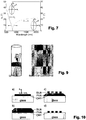
- the terahertz pulse energy from OH1 - proportional to the time integral of the square of the amplitude in Figure 7a - was 8 % larger than that from DAST.
- a significant difference between the two emitter materials is observed in the frequency spectra of their time-domain waveforms as shown in Figure 7b .
- DAST suffers from a phonon resonance centered at 1.1 THz that leads to an increased absorption and consequently to a drastically lower amplitude emitted at this frequency.
- OH1 single crystals were grown by slow evaporation of methanol as a solvent. Crystals with good optical quality were obtained with dimensions up to 4 ⁇ 4 ⁇ 2 mm 3 by the slow evaporation technique. Additionally we have grown thin films with the capillary method [23, 15] between two glass substrates with dimensions up to 3x3 mm 2 and thicknesses between 5 and 100 ⁇ m. Although, thin film growth of organic electro-optic crystals is generally a challenge and far from trivial, e.g. for DAST [24, 23], high quality OH1 thin films could be grown. X-ray analysis has shown that both bulk and thin film crystals grown from methanol, form plates with the largest surface perpendicular to the a -axis.
- the second method is based on an interferometric measurement [25, 26].
- the 1.5 mm thick sample was placed on a rotation stage in one arm of a Michelson interferometer.
- An intensity modulation as a function of the rotation angle ⁇ can be detected due to constructive and destructive interference of the two interferometric arms as the effective pathlength of the light in the crystal is changed.
- Similar to the first measurement method described above only the angles with maximum intensity were extracted and used for the determination of the refractive index.
- n 1 can be determined using p -polarized light.
- the measurement was performed at three different wavelengths, i.e. 633, 785, and 1319 nm.
- Fig. 6 shows the results obtained from both measurement methods.
- OH1 features a large birefringence for light polarized along the polar axis x 3 and the other two axes.
- ⁇ n is larger than 0.5 in the whole wavelength range up to 2.2 ⁇ m.
- the crystal is uniaxial since the refractive index n 1 matches n 2 at this wavelength.
- Fig. 7 shows a calculation of the orientation of the optical axes as a function of ⁇ . For wavelengths below ⁇ * the optical axes lie in the x 1 x 3 -plane at an angle ⁇ 2 ( ⁇ ) from the polar x 3 -axis. For ⁇ > ⁇ * the optical axes lie in the x 2 x 3 -plane at an angle ⁇ 1 ( ⁇ ).
- Table 3 Electro-optic coefficients of OH1. The electric field was applied in the x 3 -direction and modulated at a frequency of 1 kHz. The values are comparable to the largest coefficients of the well known organic salt DAST.
- the phenolic CLP chromophores were synthesized by Knoevenagel condensations according to literature. The materials were purified by recrystallization in methanol or ethylacetate.
- Powder SHG efficiency was measured at a fundamental wavelength of 1.9 ⁇ m relative to that of OH1 powder.
- ⁇ max the wavelength of the maximum absorption in methanol solution
- T i the thermal weight-loss temperature
- T m the melting temperature
- ⁇ max the maximal first-order hyperpolarizability
- ⁇ ijk eff the components of the effective non-resonant hyperpolarizability tensor in the crystallographic system.
- the investigated phenolic CLP chromophores containing different number of methyl substituents on the non- ⁇ -conjugated part of the cyclohexene ring exhibit similar wavelength of the maximum absorption ⁇ max , thermal weight-loss temperature T i and microscopic molecular nonlinearity (maximal first-order hyperpolarizability ⁇ max ).
- the microscopic molecular nonlinearity and the thermal stability are related to the length of the ⁇ -conjugated bridge and the existence of the cyclohexene ring preventing cis-trans isomerization, respectively. Therefore, the structural modifications on the non- ⁇ -conjugated part of cyclohexene ring do not affect the microscopic molecular nonlinearity and thermal stability, but only lead to different crystalline packing and macroscopic nonlinearity.
- Single crystals of the investigated phenolic CLP derivatives were grown from methanol or acetonitrile solution by the slow evaporation method at 30 or 45 °C.
- the Kurtz and Perry powder test was performed at a fundamental wavelength of 1.9 ⁇ m by measuring the reflected second harmonic generation (SHG) efficiency.
- All phenolic CLP crystals exhibit strong SHG activities.
- the powder SHG efficiency of OH3 crystals is comparable to that of OH1 crystals.
- the OH2 crystalline powder exhibits the SHG powder efficiency twice as large as OH1 powder and comparable to DAST powder. Therefore all phenolic CLP crystals investigated here are attractive for second-order nonlinear optical applications.
- phenolic CLP crystals OH2 and OH3 Single crystal structures for the phenolic CLP crystals were determined by X-ray diffraction and are given in Table 4.
- the phenolic CLP crystals OH2 and OH3 have a monoclinic with space group symmetry Cc (point group m).
- the main supramolecular interactions of the phenolic CLP crystals OH1, OH2 and OH3 are strong hydrogen bonds of C ⁇ N...H-O With the help of these two hydrogen-bonding sites at opposite ends, OH molecules build head-to-tail hydrogen bonds in the crystalline solid.
- OH2 and OH3 crystals have an isomorphic structure.
- OH2 crystals Due to highest powder SHG activities of the OH2 crystals these crystals investigated in more detail. Large size single crystals of OH2 were grown from methanol and acetonitrile solution by the slow evaporation method in an oven at 45 ° C. Orange-red crystals in the shape of plate, typically 3 ⁇ 2 ⁇ 0.5 mm in size were obtained in one week. OH2 crystals exhibit a large transparency range from 600 to 1650 nm. While OH1 crystals exhibit an absorption band at about 1.5 ⁇ m, OH2 crystals exhibit very low absorption in the optical telecommunication wavelength range (1.3-1.6 ⁇ m). The larger transparency range in the visible and the low absorption in the 1.3-1.6 ⁇ m range of OH2 crystals are of advantage for optical telecommunications and near-IR wavelength range photonic applications.
- the maximum diagonal coefficient ⁇ iii eff can be estimated as ⁇ max cos 3 ⁇ p .
- ⁇ max molecular nonlinearity
- ⁇ max of OH1 and OH2 chromophores similar molecular nonlinearity
- the maximal component of the effective hyperpolarizability tensor is larger in OH2 crystals compared to OH1 crystals.
- the amorphous glass slides were sonicated in a water/methanol mixture solution.
- a "piranha" solution H 2 SO 4 /H 2 O 2 70:30 v/v
- the substrates were rinsed repeatedly with deionized water and washed with methanol.
- the substrates were dried with argon gas. This procedure resulted in OH-modified substrates.
- 3 mM of 4-trichlorosilyl butyronitrile and octadecyltrichlorosilane in chloroform were prepared. Then, the OH-modified substrates were immersed for 3 h. They were washed and sonicated in chloroform.
- OH1 solution with a concentration of 0.1 g OH1 in 100 ml methanol was prepared in a small glass bottle.
- the substrates were leaning in the solution against the glass wall at an angle of about 25°, as shown in Fig. 9a .
- the bottles with OH1 solution and a slide glass were kept in an oven at 38°C and were not completely closed, leading to the evaporation of the solvent at a rate of about 4 ml/day. As the solvent was evaporating, the OH1 crystal was growing along the surface of substrates ( Fig. 9a ).
- OH1 crystals grew nicely on the upper part of the glass substrate.
- the grown thin-film crystals show large single crystalline domains of above 150 mm 2 with high optical quality ( Fig. 9b ).
- the thicknesses ranged from 5 to 20 ⁇ m.
- Substrates with pre-fabricated electrodes were also used for thin film growth.
- the normal slide glasses were patterned with gold electrodes and subsequently cleaned by piranha solution.
- the growth procedures were as above.
- Thin OH1 single crystalline films grew on gold-patterned substrate ( Fig. 28d ).
- the crystals grow with their polar axis parallel to the substrate.
- the grown thin film crystals were manually polished to ⁇ /4 surface quality. This step resulted in a homogenous, planparallel, and high optical quality thin film with a thickness of 3-4 ⁇ m that were further used for waveguide fabrication.
- the OH1 solutions in methanol were prepared with different concentrations and filtered through filter paper.
- the substrates having modified surfaces were immersed at an angle of about 30° from the vertical direction in the OH1 methanol solutions in a cylindrical container of 4 cm diameter.
- the containers were placed in an oven of constant temperature (40 °C).
- the methanol solvent evaporated slowly at a rate of about 2 mL/ day and OH1 crystals nucleated and grew on the modified substrates.
- the thickness of the films was determined by a Tencor Alphastep P11 profilometer.
- hydrophilic glass substrates functionalized with -OH and -CN groups by piranha solution treatment and silanization with 4-trichlorosilyl butyronitrile, respectively. Since the OH and CN groups are the hydrogen bonding donor and acceptor sites in OH1 crystals, the OH- and CN-modified surfaces can act as a mimic crystal surface and can interact with OH1 molecules. For comparison, hydrophobic CH 3 -modified glass substrates were also prepared by silanization with octadecyltrichlorosilane.
- Single crystalline thin films of OH1 were grown from methanol solution on the modified substrates. Different from the growth techniques using a capillary effect occurring between two glass substrates only one substrate was used. This substrate was immersed at an angle of about 30° from the vertical direction in the OH1 methanol solution in an oven at constant temperature (40 °C).
- the solutions had a very low concentration, typically 1 order of magnitude lower (0.1-0.6 g of OH 1/100 g of methanol) than the saturated concentration (3.74 g of OH 1/100 g of methanol at 40 °C) to prevent spurious nucleation in the solution.
- OH1 crystals first nucleated and then continued to grow on the modified substrates.
- the resulting OH1 crystals grown directly on amorphous modified substrates are shown in Fig. 28 .
- the OH1 crystals grew very well and fully covered the OH- and CN-functionalized substrates (see Fig. 28a,b ).
- OH1 crystals did not grow, forming only small amorphous droplets (see Fig. 28c ).
- the reason for the nucleation is an enhanced evaporation in this wetting layer compared to the rest of the solution and the concentration in this region may become locally supersaturated.
- OH1 molecules having strong hydrogen bond donor OH sites and acceptor CN sites strongly interact with hydrogen bond donor OH groups or acceptor CN groups on the modified surface of the substrates. Therefore, by evaporation-induced local supersaturation in the wetting layer on strongly hydrophilic substrates and strong specific interactions between OH1 molecules and modified substrates, the first few thin nuclei are formed at the top of the wetting layer. After forming the first nuclei, OH1 molecules continue to crystallize following the evaporation direction on the substrate.
- the molecules are continuously supplied by the concentration difference between the wetting layer and bulk solution (see Fig. 27a ). Since the growth is seeded by the first nuclei, the concentration of the solution in the wetting layer remains within the solution metastable zone, and therefore further spontaneous nucleation does not occur anymore on the substrate as well as within the solution.
- Our investigations show that the metastable zone of the OH1/methanol system is relatively large, and therefore this condition is easy to achieve. This allows for growing crystals with very large-area single domains having essentially unlimited domain length.
- the OH1 solution has a larger contact angle, and the liquid-solid surface tension is higher than on CN- and OH-modified surfaces (see Fig. 27b ).
- the air-solution interface moves down by solvent evaporation, the meniscus area is stretched and the meniscus is unstable. As a consequence, the meniscus is either split into a droplet and a new meniscus, or the contact line of the meniscus just slips down.
- the CH 3 -functionalized surface cannot interact with OH1 molecules. Therefore, as shown in Fig. 28c , OH1 crystals did not grow on the CH 3 -functionalized substrates.
- OH-modified surfaces can be easily prepared by piranha solution, while CN-modified surfaces need the piranha treatment and also silanization that is sensitive to humidity and the content of impurities. Therefore, using OH-modified substrates for large-area single-crystalline thin films of OH1 results in a facile process without any additional complicated procedure.
- X-ray diffraction patterns were recorded in the reflection mode. As shown in Fig. 29a , very sharp peaks were observed, indicating a high crystalline quality.
- the Bragg peaks could be assigned to (200), (400), (600), (800), and (1000) crystallographic planes. Therefore, the large crystal surface corresponds to the bc crystallographic plane, and due to the orthorhombic crystal system of the crystals, the a -axis is perpendicular to the surface of the thin films.
- the OH1 crystals on the substrates grow normal to the crystallographic a -axis direction and form specific interactions with hydrogen bonds as illustrated in Fig. 29b .
- We determined the directions of the b- and polar c-axes by measuring the change of the transmittance under crossed polarizers.
- the optical principal axis with a lower transmission for light polarized along it is the polar c-axis.
- the polar c-axis is oriented along the evaporation direction (growth direction) of the solvent with a small variation for different single-crystalline domains (up to 20 degree). This can be related to the fact that the growth rate of OH1 is the fastest along the polar axis direction. Therefore domains with the polar axis matching the growth direction will predominate.
- Fig. 30 shows a transmittance spectrum of the single crystalline domain on the OH-modified substrate for light polarized along the c-axis, using a pinhole of about 1 mm diameter.
- the spectrum shows interference fringes due to the multiple reflections of light at the film/air and film/substrate interfaces. This confirms that the films are of high optical quality without noticeable scattering centers.
- the thickness of the films can be controlled by the concentration of the solution.
- Fig. 31 shows the measured film thickness as a function of the concentration of the initial solution. We observed that the thickness of the films is generally larger for higher concentrations of the initial solution.
- the thickness variation becomes smaller with an increase in the initial solution concentration, which indicates that one can most likely avoid the thickness variation by properly adjusting the growth conditions (concentration, temperature, tilt angle) to achieve the mass balance, that is, to match the growth and the solvent evaporation rate to the amount of the material in the solution. Nevertheless, this small thickness variation is not relevant for integrated electro-optic modulators in our case, since for the optimized electrode configurations waveguides are aligned perpendicularly to the polar c-axis, where there are no thickness variations. Using the thin films grown as presented above, we have successfully fabricated single crystalline waveguides and already demonstrated efficient electro-optic modulation.
- the ELSSI method may be applicable to other organic crystals, as long as they can nucleate and grow well from the solution, as well as have a large enough metastable zone to avoid spontaneous nucleation during growth. Obviously the growth parameters and substrate surface properties need to be adjusted for a different material/solution system.
- the waveguide pattern was then transferred into the crystal by reactive-ion etching (RIE).
- RIE reactive-ion etching
- Organic materials can be etched with high etch rates using oxygen as reactive agent. Since both, resist and crystal are organic compounds it is important to optimize the etch process for OH1, thereby obtaining the best selectivity against SU8.
- the etch rate of OH1 could be substantially increased by adding CF 4 to the oxygen as etch gas.
- Fig. 12 shows the etch rate of OH1 as a function of the CF 4 concentration.
- the total gas flow was 52 sccm for all combinations of gases, while the chamber pressure was kept at 200 ⁇ bar for the experimental determination of the etch rates.
- the forward rf-power was set to 200 W.
- etch rate exhibits a sharp maximum at a gas flow ratio of CF 4 : O 2 ⁇ 23%. At this point an etch rate selectivity of OH1 against SU8 of approximately 1:1.35 was obtained.
- a lower chamber pressure of 25 ⁇ bar with the same ratio of etch gases. This led to a lower etch rate with the same selectivity between crystal and resist and an improved surface quality of OH1.
- the etch time was adjusted in order to fully etch away the remaining resist and PVA protection layer on the waveguides.
- the absorption coefficient, as measured in OH1 bulk crystals leads to a loss of 46 dB/cm for TE modes and 13 dB/cm for TM modes, assuming ⁇ 1 ⁇ 2 . In the range from 800 nm up to 1400 nm light is only very weakly absorbed by OH1 enabling the fabrication of potentially efficient waveguides with losses below 1 dB/cm.
- the scattered light is proportional to the guided light intensity I ( z ) at all positions z along the waveguide, and the propagation loss ⁇ can be calculated by analyzing the variation of the scattered light intensity.
- the electric field inside the waveguide with the given electrode configuration was calculated with the simulation package Femlab from COMSOL.
- the electric field in the guiding material is smaller than in the air due to the difference in the dielectric constant ⁇ r .
- ⁇ r ; x 3 5.26 as the dielectric constant along the polar axis of OH1, which is an extrapolated value from THz-frequency range measurements.
- the results of the electro-optic coefficient measurement and the calculated average electric field in the waveguide are given in Table 6. We have obtained a little more than 70% of the bulk values we measured.
- the geometry of the electrodes has not been optimized and can be considerably improved by reducing the electrode spacing d.
- a cladding with a similar dielectric constant as OH1 will further reduce the half-wave voltage of the device.
- the proposed geometry leads to an increase of the electro-optic efficiency by a factor of more than 20. Consequently, a reduction of the half-wave voltage ⁇ length product V ⁇ ⁇ L to 0.39 Vcm and 1.3 Vcm at the wavelengths of 632.8 nm and 852 nm may be achieved, respectively, based on the r-coefficient we have determined experimentally. With such waveguides it is therefore possible to combine low driving power with extremely fast response of organic materials, which should enable switching and modulation at a high rate of up to 200 GHz and above.
- the first step is to pattern the waveguide geometry in a substrate material and to equip it with electrodes.
- a cover is anodically bonded to the substrate to delimit the volume for the crystallization of the EO active material.
- material powder is placed on the substrate at the edge of the cover and melted such that the melt can flow through the waveguide channels into the structure and crystallize there.
- chromium and 50 nm amorphous silicon were deposited on a borosilicate glass wafer by standard photolithographic processing, and a standard lift-off technique (see Fig. 14a ).
- the chromium was used as electrical contacts to the waveguide in the final structure and silicon was required for anodic bonding.
- grooves with typical dimensions of 1.5-5 ⁇ m width were structured in-between the electrodes into the commercial photoresist AZ6632 and then transferred to the borosilicate substrate wafer by subsequent reactive ion etching (see Fig. 14b ).
- a cover borosilicate glass shorter than the length of the structured grooves was anodically bonded to the structured substrate wafer, such that the left and right ends of the grooves in the substrate protruded from the edges of the cover glass and the material melt could flow in (see Fig. 14c ).
- Anodic bonding is one of a number of techniques used in the semiconductor industry for wafer bonding [31, 32, 33]. It is well-established and was in 2004 reported to account for the majority of all packaging applications for microelectromechanical (MEMS) devices [33].
- the substrate and cover material is a commercial standard borosilicate glass suitable for anodic bonding to silicon due to a thermal expansion coefficient that matches the one of silicon in order to avoid thermal stress.
- the borosilicate wafers had a thickness of 200 ⁇ 25 ⁇ m, an averaged roughness of the surface of less than 1.5 nm and a total thickness variation of less than 10 ⁇ m.
- the anode of a high voltage power supply was contacted to the deposited chromium and the cathode to a wolfram plate pressed slightly against the cover glass.
- the bonding process was performed at a temperature of 456°C by applying a dc voltage of 700 V to the two electrodes.
- the silicon deposited on top of chromium acts as a sodium diffusion barrier. It has been shown that in similar geometries also very thin layers of 20 nm silicon are sufficient as sodium diffusion barriers [34].
- the aluminium stripe attached to one side of the sample should ensure an asymmetry in the temperature profile along the channels to prevent several nucleation points.
- the total growth time is with less than eight hours relatively short, which is another advantage compared to e.g. solution grown thin films that typically require 2-10 weeks growth time [15].
- SEM scanning electron microscopy
- slotted silicon waveguide configurations allow for a considerable improvement of the tunability of EO modulators, sensors and all-optical switching devices over the current state of the art [35, 36].
- the essential feature of a slot waveguide is that two high-index silicon stripes are separated by a small distance on the order of 20-140 nm filled with a lower-index material.
- the optical field intensity in such a structure tends to concentrate within the low-index slot for the polarization perpendicular to the slot. Therefore and also due to the close proximity of the electrical contacts in a slotted geometry filled with a EO active material, a very large refractive index change for a given modulation voltage can be obtained compared to a more conventional waveguide with external electrodes.
- the nanometer size channels were realized with a simple one-layer approach and a standard lift-off process.
- the commercial photoresist ma-N 415 was spin coated on the borosilicate substrate.
- a standard UV lithography process was performed to generate the required ridges in the photoresist with widths between 3 and 11 ⁇ m .
- Approximately 20 nm silicon was then deposited preserving the undercut for subsequent lift-off.
- the fabricated pattern in silicon was terminated by anodic bonding of a second borosilicate wafer to the structure and the crystals grown in these structures as described in the previous section.
- a microscope image and a scanning electron micrograph of the grown crystals are shown in Fig. 16 and 17 respectively.
- a crystal thickness of approximately 25 nm perpendicular to the c-face corresponds, according to the unit cell parameters, to only approximately a dozen unit cells in this direction.
- the lateral crystalline dimension of the reported nanowires could be increased by two orders of magnitude and therefore the growth of ultra-thin large-area crystals was possible as well.
- the processing to achieve these nanosheets was analogous to the one depicted in Fig. 14 , except that the chromium-silicon bonding areas were structured much further apart, such that channel dimensions of about 90 nm height and 0.5 mm width were formed. Inspection of the grown nanosheets under the microscope between crossed polarizers showed that the crystal orientation is usually preserved for domain sizes on the order of 10'000 ⁇ m 2 . In these preliminary experiments small gaps within the nanosheets appeared (black spots in Fig. 18 ), where crystalline material is absent.
- the nanosheets produced in this way are highly interesting also because with their help the crystals can be grown in closed waveguide configurations, such as microrings (see Fig. 18 ) and photonic crystal structures .
- Waveguide structures of any shape can be fabricated by RIE in the substrate borosilicate wafer (analogously to the straight waveguide structuring in Fig. 14 ) and they can be filled by flowing the melt through the nanosize channels to the fabricated structure.
- the orientation of the crystal in the waveguide-structure is determined by the corresponding single crystalline domain of the nanosheet.
- the demonstration of electro-optical amplitude modulation in such structures proves, for the first time to our knowledge, the compatibility of crystalline materials with the silicon-photonics technology.
- the experimental determined half-wave voltage V ⁇ ⁇ L is 45 ⁇ 10 Vcm, in agreement with theory.
- An optimized electrode-waveguide system can further reduce V ⁇ . L to 2.0 Vcm for TM-modes and even 0.17 Vcm for TE-modes.
- the proposed cladding modulation significantly reduces fabrication complexity of crystalline electro-optic waveguides, compared to previously developed techniques.
- the attachment of the active cladding material is generally applicable to a wide range of crystalline materials.
- crystalline electro-optic materials feature an excellent long term stability of the chromophore orientation, superior photochemical stability, and do not require high-field poling prior to operation.
- Silicon-on-insulator nanowire waveguides are very attactive for very large scale photonic integrated circuits (PICs) [37, 38]. Due to the high index contrast between Si and SiO 2 , compact splitters, couplers and micron-sized bend radii can be realized. Various passive linear functions such as wavelength division multiplexing (WDM) filters based on arrayed waveguide gratings (AWGs) [39] as well as microring resonators (MRRs) [40] have been demonstrated. Another advantage of this technology is its close relation to complementary metal-oxide semiconductor (CMOS) technology, which allows the application of its matured processes and the access of its huge knowledge base. Integrated optics in silicon is also interesting for cost reasons.
- CMOS complementary metal-oxide semiconductor
- Silicon-on-insulator wafers are considerably more attractive in price compared to more exotic materials such as the III-V semiconductor compounds or the insulator LiNbO 3 .
- Phase modulators in SOI rib waveguides have been fabricated for many years [41]. However, these modulators are based on current injection, which keeps the bandwidth within the GHz region. This limitation does not meet todays requirements for high-speed optical communication. Nano-slot waveguides have been proposed in combination with an electro-optic polymer cladding in order to reduce modulation voltages by orders of magnitude [42]. However, technological difficulties and stability issues with the polymers involved have led to moderate success up to date.
- Type a) is the conventional one, in which the waveguide core material is electro-optically active. This modulation scheme is used most often, for example in commercial LiNbO 3 high-speed modulators.
- the other two types b) and c) can be directly combined with the highly advanced SOI technology.
- Cladding modulation is the scheme used for type b), where an electro-optic refractive index change in the cladding material results in a change of the effective index, corresponding to the guided mode in the SOI waveguide structure.
- Type c) is a non-conventional waveguide structure, in which the modal intensity is enhanced in the sub-100 nm wide slot consisting of the active material embedded in a silicon wire single-mode waveguide [43].
- the silicon structures can be used as electrodes, provided they are adequately conductive. Especially for type c), this can lead to high electric fields for low applied switching voltages [42].
- FIGS 20 a) and b ) show the simulated intensity distribution for the type b) and c) waveguide structures with a typical refractive index of an organic electro-optic cladding material ( n ⁇ 1.6).
- n an organic electro-optic cladding material
- the advantage of the slotted structure in Fig. 20 b) is the strong modal confinement and high light intensity in the active material, which is especially interesting for higher order nonlinear optical effects that are intensity dependent.
- the narrow slot functioning as the gap between the two silicon ridge electrodes, results in high electric field strength for comparably small applied voltages. This leads to a high electro-optic refractive index change at small modulation voltages.
- the advantages of the slotted waveguide structure come at the expense of the technological difficulties of patterning narrow slots into the silicon below the resolution capabilities of standard optical lithography processes, and filling the slots homogeneously with an appropriately ordered electro-optic material.
- MZ Mach-Zehnder
- Fig. 19 Due to the favorable growth properties of OH1, it was chosen as the active cladding material for Mach-Zehnder (MZ) modulators of type b) in Fig. 19 .
- the crystalline thin films grow with their x 1 -axis perpendicular to the substrate surface.
- the direction of the polar axis can be controlled by the growth process described above.
- the ideal alignment is the one with the polar x 3 -axis perpendicular to the electrodes on both sides of the waveguides, which results in the deployment of the electro-optic coefficient r 113 and r 333 for TM- and TE-modes, respectively.
- the sensitivity factor ⁇ n i ⁇ n eff / ⁇ n i
- n i is an important term in the context of electro-optic cladding modulation, since it determines the efficiency of the change in effective index ⁇ n eff of a guided mode as a result of the refractive index change of the cladding material ⁇ n i .
- Fig. 21 b) shows the modulation efficiency ⁇ n i as a function of the silicon core height h , taking into account the material parameters of OH1.
- the TM-mode is more advantegous than the TE-mode, reaching efficiencies as high as 80% for silicon heights below 180 nm.
- Silicon-on-insulator wafers from Soitec were used as starting material for the fabrication of integrated MZ-type modulators.
- the substrate featured a single-crystalline Silicon layer with a thickness of 200 nm.
- the thickness of the buried oxide was 2 ⁇ m.
- the process steps of the device fabrication are depicted in Fig. 22 .
- a) Waveguides and MZ-structures were patterned using standard optical lithography processes using ma-N 1410 as a negative photoresist.
- the patterns in the resist were transferred into the SOI-layer by reactive-ion etching (RIE) on a machine from Oxford Instruments (Plasmalab 80).
- RIE reactive-ion etching
- Total etching time for an etch depth of 240 nm at 200 W forward power was 12 min.
- a combination of different etch gases was used including O 2 , Ar, CF 4 and CHF3.
- a mask aligner from Karl Süss (MA6) was used for the alignment and exposure of the positive photoresist (AZ 6632) with a sufficient thickness for metal lift-off.
- the oxide was necessary to reduce reflections and guiding losses in the regions where the electrodes cross the waveguides in order to contact the inside of the MZ-structures.
- Metal lift-off was performed in an ultrasonic bath in acetone, revealing the MZ-structures shown in Fig. 23 .
- the interaction length within the MZ-interferometer was 0.5 mm long.
- Large-domain, single-crystalline OH1 was subsequently grown directly onto the prepared substrates with the dielectric x 1 -axis of the crystal normal to the substrate surface. The growth details are described above, leading to 2-5 ⁇ m thick single-crystalline thin films with their polar x 3 -axis directed perpendicular to the electrodes.
- the device was covered with a 2 ⁇ m thick, spin coated polyvinyl alcohol (PVA) protection layer.
- PVA polyvinyl alcohol
- the waveguides were wider than the ideal wire width of w ⁇ 400-500 nm with the consequence of allowing multiple modes to propagate.
- the cladding modulation efficiencies for these structures have been determined numerically.
- wire widths w >1 ⁇ m the efficiencies for the first guided mode remain constant, as shown in Fig. 24 .
- the efficiency for TE fundamental modes is considerably smaller due to the strong confinement of the light intensity for this polarization.
- the integrated MZ-interferometers were analyzed using a standard end-fire coupling setup.
- a sinusoidal modulation signal V(t) was applied to the electrodes of the MZ-structures.
- the modulation signal generated by the photodiode was visualized on an oscilloscope.
- Table 8 contains the calculated half-wave voltages, considering a field overlap ⁇ 1.
- ⁇ n i The cladding modulation efficiency ⁇ n i is given by ⁇ n eff / ⁇ n i
- Exp Experimental device.
- Ideal Proposed MZ-structure with single-mode SOI wire waveguides. Mode ⁇ ni ; exp [%] V ⁇ ,exp ⁇ L [Vcm] ideal w ⁇ h [nm ⁇ nm] ⁇ n i ; ideal [%] V ⁇ ,ideal ⁇ L [Vcm] TM 60 31 ⁇ 1 400 ⁇ 180 80 2.0 TE 13 9 ⁇ 1 400x150 60 0.17
- Electro-optic amplitude modulators based on integrated Mach-Zehnder interferometer structures with single crystalline OH1 as cladding material.
- Silicon-on-insulator wafers were used with a 200 nm thick SOI layer.
- the waveguide structures were patterned with conventional optical lithography, producing waveguides with widths of 3 ⁇ m and up.
- multimode waveguides were used with the advantage of a simpler fabrication using optical lithography.
- the interferometer arms were 0.5 mm long and electrodes were deposited on both sides of the waveguide with a total gap of 7 ⁇ m.
- OH1 was chosen as cladding material, since it offers the possibility of growing single crystalline thin films on top of the integrated photonic structures.
- Mode-solver simulations have shown that the TM- and TE-modes guided by the silicon wires exhibit a high efficiency for cladding modulation.
- a refractive index change in the cladding material results in a high change in effective index of the guided fundamental mode with an efficiency of up to 80% in the ideal configuration. This is due to the fact that considerable modal intensity is guided outside the waveguide core.
- Electro-optic modulation has been demonstrated in various operation points on the switching curve.
- This result proves the compatibility of the electro-optically active organic material OH1 with the highly advanced passive SOI technology.
- This work demonstrates an interesting way how to exploit the advantages of the passive SOI technology in combination with the ultra-fast electro-optic activity in organic crystalline materials, with highly stable chromophore orientation.
- An optimized waveguide-electrode structure which can be obtained using e.g.
- e-beam lithography has the potential to decrease the half-wave voltage ⁇ length product to 2 Vcm and even to 0.2 Vcm for TM- and TE-modes, respectively.
- the modulation bandwidth can be extended beyond the limits of todays commercially available modulators based on LiNbO 3 , due to the ultra-fast electro-optic response, previously demonstrated in OH1 as a THz-wave emitter.
- the proposed configuration for cladding modulation can be readily applied to other crystalline materials and circumvents technological issues present in the context of slotted waveguide structures as well as conventionally fabricated active waveguides.
- the metastable-zone width is a very important parameter for both inducing the nucleation and growth of high optical quality and large size single crystals.
- the metastable zone width for OH1 in methanol is very large, around 40°C, as shown in Fig. 25 . (For example, for the benchmark DAST crystals in methanol the metastable zone is only about 7°C wide in the same temperature range).
- the very large metastable-zone width is related to strong hydrogen-bonding interactions between the OH1 molecules and the methanol molecules. Table 9. Solubility of OH1 in different solvents (g /100g solvent). Acetone Acetonitrile Ethanol Methanol Methylene chloride 25 °C 25.9 4.32 2.34 2.15 1.4 40 °C 41.8 5.3 2.5 3.4 1.9
- nucleation in an impurity-free solution at a certain temperature will easily appear only when the solution concentration exceeds the upper boundary of the metastable zone.
- nucleation is achieved in the following way: starting from the saturated solution, the solvent is left to evaporate at a constant temperature or the temperature of the solution is decreased; nucleation will appear after the solution concentration exceeds the metastable zone boundary.
- the nucleation will be induced at the air/solution/container interfaces and also solution/container interfaces.
- the spontaneously nucleated crystals of OH1 can be grown with a different morphology depending on the nucleation conditions. Thin crystals will be obtained if the supersaturation is low (lower than 0.05), while thicker crystals will appear at higher supersaturations. The thickness will also depend on the number of nuclei (which will affect the supersaturation ratio), which can be controlled by the interface or impurity conditions, as well as the evaporation rate.
- Slow evaporation method can yield in case of OH1/methanol large-area (1 cm 2 and more) crystals with a high optical quality, but the thickness limited to a few mm.
- Thicker crystals (up to 1cm and more) of a high optical quality can be grown by a slow cooling method from a seeded solution. For this: Best seed crystals grown by spontaneous nucleation are chosen. Several crystallographic faces can be observed on these crystals, as shown in Fig. 26 .
- a seed crystal is attached to a holder, so that their -c side (see Fig. 26 ) is at the holder.
- the seed will grow mostly along the (0,1,1) and (0,-1,1) faces and in thickness (along the ⁇ a direction).
- the morphology can be controlled by choosing an appropriate cooling rate. Because of the high metastable zone width, there is a lot of freedom in choosing different supersaturation ratios during the growth; the concentration should only remain within the wide metastable zone ranges of the seeded solution to keep the high optical quality of the grown crystals. In general, a higher supersaturation ratio (achieved by a faster cooling rate) will give thicker OH1 crystals.
- the morphology of these crystals can be also modified by using other solvents or solvent combinations, e.g. methanol/ethanol mixtures. This will modify the phase diagram and therefore the growth characteristics.
- OH1 crystals having side lengths of more than 1 cm and high optical quality can be grown very fast, in less than 1 week, by either slow evaporation or slow cooling methods. (For example, for the benchmark DAST crystal this time is 4-6 weeks).
- Bulk and thin-film phenolic CLP crystals can be used for second-order nonlinear optical applications, such as frequency conversion, including terahertz wave generation (see Fig. 32 ), and electro-optic applications, including high-speed switching and modulation and integrated photonic structures, such as those illustrated in Fig. 33 .
- Fig. 32 shows: a) Schematic of terahertz-wave generation by difference-frequency generation, where two optical waves having closely spaced wavelengths ⁇ 1 and ⁇ 2 interact in a phenolic CLP crystal to generate a single-frequency terahertz wave, whose frequency can be tuned by tuning the wavelength of one or both of the pumping beams. b) Schematic of terahertz-wave generation by optical rectification, where various frequency components of a short pump optical pulse interact in a phenolic CLP crystal to create a broadband terahertz signal.
- Fig 33 a) The basic design of a microring resonator consists of a circular waveguide coupled to a straight port waveguide. b) Schematic view of a microring resonator with two port waveguides. c) Schematic drawing of a Mach-Zehnder interferometer. d) Combination of a microring resonator and a Mach-Zehnder interferometer. e) Schematic representation of a microring-resonator array in an optical network acting as active wavelength division multiplexer. f) Schematic of a photonic crystal waveguide modulator. Phenolic CLP crystal is used either as core waveguiding material or as active cladding material of higher-index waveguides (like silicon wires) or embedded inside slotted higher-index waveguides.
Landscapes
- Physics & Mathematics (AREA)
- Nonlinear Science (AREA)
- General Physics & Mathematics (AREA)
- Optics & Photonics (AREA)
- Optical Modulation, Optical Deflection, Nonlinear Optics, Optical Demodulation, Optical Logic Elements (AREA)
Claims (13)
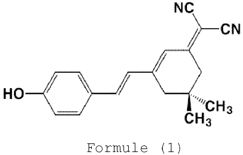
- Film mince monocristallin disposé sur un substrat prévu pour des applications optiques non linéaires, le film mince monocristallin étant constitué d'un composé de polyène à configuration bloquée présentant un donneur d'électrons phénolique, le composé étant représenté par la formule (1)

- Film mince monocristallin selon la revendication 1, dans lequel le substrat est un substrat amorphe ou cristallin et le film mince monocristallin a une superficie > 150 mm2 et une épaisseur comprise entre 0,05 et 20 µm.
- Procédé pour faire croître un film mince monocristallin d'un composé de polyène à configuration bloquée présentant un donneur d'électrons phénolique, le composé étant représenté par la formule (1)
 - prévoir un ou plusieurs substrats, au moins une surface du ou des substrats étant une surface hydrophile,- appliquer le composé dissous dans un solvant sur la ou les surfaces du substrat,- faire croître un film mince monocristallin sur une ou plusieurs surfaces du ou des substrats en mouillant la ou les surfaces avec la solution grâce aux forces capillaires ou d'adhérence et permettre sur la ou les surfaces une sursaturation locale induite par évaporation,
la ou les surfaces hydrophiles du ou des substrats étant une ou plusieurs surfaces modifiées par OH ou CN. - Procédé selon la revendication 3, dans lequel le substrat comprend : un semiconducteur tel que le silicium (amorphe ou cristallin) ou un semiconducteur III-V (par exemple GaAs, InP, AlGaAs), du verre à base de silice, par exemple un verre au silicate (SiO2) ou un verre au borosilicate, un polymère tel que le polyméthacrylate de méthyle (PMMA), un polycarbonate (amorphe), le téflon (polytétrafluoroéthylène), un polymère à base de benzocyclobutène (BCB) et/ou un polymère minéral-organique hybride.
- Procédé selon l'une des revendications 3 ou 4, dans lequel l'étape consistant à prévoir un substrat comprend l'obtention d'un substrat préfabriqué qui comprend une surface structurée par un ou plusieurs creux et/ou une surface structurée par un ou plusieurs éléments en saillie, la surface comprenant facultativement des éléments électriquement conducteurs, en particulier des anodes, le substrat comprenant facultativement deux ou plusieurs couches en matériaux différents et l'étape de croissance de cristaux sur la ou les surfaces du substrat comprenant la croissance des cristaux dans le ou les creux et/ou sur les parties de surface qui entourent le ou les éléments en saillie.
- Procédé selon l'une des revendications 3 à 5, dans lequel deux substrats séparés par un petit interstice sont prévus, le composé est appliqué à l'état fondu et le film mince monocristallin est mis à croître dans le petit interstice.
- Procédé pour faire croître une masse de film mince monocristallin d'un composé de polyène à configuration bloquée présentant un donneur d'électrons phénolique, le composé étant représenté par la formule (1)
 - prévoir le composé dissous dans un solvant, de préférence le méthanol,- prévoir un cristal d'inoculation relié à un support de telle sorte que le côté -c du cristal d'inoculation soit relié au support à l'intérieur de la solution,- contrôler la morphologie du cristal en contrôlant au moins la vitesse de refroidissement.
 - Procédé selon la revendication 7, dans lequel le cristal d'inoculation est mis à croître par nucléation spontanée induite par une particule étrangère ou par une fluctuation induite de l'extérieur.
- Élément optique intégré ou dispositif optique non linéaire, en particulier pour la commutation optique, le filtrage optique ou la modulation optique, y compris les applications à grande vitesse, ou pour la conversion de fréquences, y compris la production et la détection d'ondes de l'ordre des THz, en particulier un dispositif photonique tel qu'un guide d'ondes, un coupleur directionnel, un résonateur à micro-anneau, une structure à bande photonique interdite, un commutateur optique, un filtre optique, un modulateur optique, un élément de détection, un détecteur de champ, un convertisseur de fréquences, de préférence un convertisseur de fréquences servant à la détection de rayonnement infrarouge, infrarouge lointain ou de l'ordre des THz, comprenant un film mince monocristallin sur un substrat fabriqué en recourant à un procédé selon l'une des revendications 1 à 3 ou un monocristal massif fabriqué en recourant à un procédé selon l'une des revendications 7 ou 8.
- Élément optique intégré selon la revendication 9, dans lequel le substrat comprend : un semiconducteur tel que le silicium (amorphe ou cristallin) ou un semiconducteur III-V (par exemple GaAs, InP, AlGaAs), du verre à base de silice, par exemple un verre au silicate (SiO2) ou un verre au borosilicate, un polymère tel que le polyméthacrylate de méthyle (PMMA), un polycarbonate (amorphe), le téflon (polytétrafluoroéthylène), un polymère à base de benzocyclobutène (BCB) et/ou un polymère minéral-organique hybride.
- Élément optique intégré selon les revendications 9 ou 10, dans lequel le substrat est un substrat préfabriqué qui comprend une surface structurée par un ou plusieurs creux et/ou une surface structurée par un ou plusieurs éléments en saillie, la surface comprenant facultativement des éléments électriquement conducteurs, en particulier des anodes, le substrat comprenant facultativement deux ou plusieurs couches en matériaux différents.
- Élément optique intégré selon la revendication 11, dans lequel le substrat préfabriqué est un substrat doté d'un ou plusieurs creux, de préférence un substrat en verre et dans lequel la couche monocristalline est agencée dans le ou les creux de telle sorte que la couche monocristalline joue le rôle du matériau d'âme d'un guide d'ondes et le substrat joue le rôle du placage du guide d'ondes, ou un substrat doté d'un ou plusieurs éléments en saillie, de préférence en silicium, la couche monocristalline étant agencée autour du ou des éléments en saillie de telle sorte que l'élément en saillie joue le rôle du matériau d'âme d'un guide d'ondes et la couche monocristalline le rôle du placage du guide d'ondes.
- Élément optique intégré selon les revendications 9 à 12, comprenant en outre une ou plusieurs structures électriquement conductrices servant d'électrode et capables de moduler les propriétés optiques de la couche monocristalline par effet électro-optique induit par l'application d'une tension électrique.
Priority Applications (1)
| Application Number | Priority Date | Filing Date | Title |
|---|---|---|---|
| EP09741647.3A EP2291712B1 (fr) | 2008-05-06 | 2009-05-05 | Monocristaux volumineux de polyène phénolique à configuration figée, couches minces cristallines et guides d'ondes optiques destinés à des applications électro-optiques et d'ondes thz |
Applications Claiming Priority (3)
| Application Number | Priority Date | Filing Date | Title |
|---|---|---|---|
| EP08008483 | 2008-05-06 | ||
| PCT/CH2009/000142 WO2009135329A1 (fr) | 2008-05-06 | 2009-05-05 | Monocristaux volumineux de polyène phénolique à configuration figée, couches minces cristallines et guides d'ondes optiques destinés à des applications électro-optiques et d'ondes thz |
| EP09741647.3A EP2291712B1 (fr) | 2008-05-06 | 2009-05-05 | Monocristaux volumineux de polyène phénolique à configuration figée, couches minces cristallines et guides d'ondes optiques destinés à des applications électro-optiques et d'ondes thz |
Publications (2)
| Publication Number | Publication Date |
|---|---|
| EP2291712A1 EP2291712A1 (fr) | 2011-03-09 |
| EP2291712B1 true EP2291712B1 (fr) | 2021-06-02 |
Family
ID=40796212
Family Applications (1)
| Application Number | Title | Priority Date | Filing Date |
|---|---|---|---|
| EP09741647.3A Active EP2291712B1 (fr) | 2008-05-06 | 2009-05-05 | Monocristaux volumineux de polyène phénolique à configuration figée, couches minces cristallines et guides d'ondes optiques destinés à des applications électro-optiques et d'ondes thz |
Country Status (3)
| Country | Link |
|---|---|
| US (1) | US8846969B2 (fr) |
| EP (1) | EP2291712B1 (fr) |
| WO (1) | WO2009135329A1 (fr) |
Families Citing this family (15)
| Publication number | Priority date | Publication date | Assignee | Title |
|---|---|---|---|---|
| KR20130024365A (ko) * | 2011-08-31 | 2013-03-08 | 아주대학교산학협력단 | 비선형 광학용 퀴놀리늄 단결정 |
| EP2881780A1 (fr) * | 2013-12-03 | 2015-06-10 | Karlsruher Institut für Technologie | Matériau optique non linéaire de second ordre |
| CN104007566B (zh) * | 2014-05-23 | 2017-03-29 | 首都师范大学 | 一种基于有机聚合物薄膜的太赫兹波调制器 |
| CN104860879B (zh) * | 2015-04-15 | 2017-03-22 | 齐鲁工业大学 | 一种丙二腈异佛尔酮类铜离子荧光探针及其制备方法 |
| KR101735191B1 (ko) * | 2015-07-08 | 2017-05-12 | 경북대학교 산학협력단 | 화합물 및 시아나이드 이온, 아민계 화합물 또는 구리 이온 검출용 화학 센서 |
| US9995875B2 (en) | 2015-07-28 | 2018-06-12 | The Penn State Research Foundation | Method and apparatus for producing crystalline cladding and crystalline core optical fibers |
| WO2017031366A1 (fr) * | 2015-08-19 | 2017-02-23 | President And Fellows Of Harvard College | Méta-réseaux efficaces multifonctionnels à bande large basés sur des déphaseurs de guides d'ondes diélectriques |
| CN111051409B (zh) * | 2017-08-06 | 2022-12-27 | 阿里尔科学创新有限公司 | 聚合物结晶组合物及其制造方法与用途 |
| US11740399B2 (en) * | 2018-02-06 | 2023-08-29 | Raytheon Company | Low cost dispersive optical elements |
| CN111965858B (zh) * | 2020-08-25 | 2024-02-02 | 济南晶正电子科技有限公司 | 一种电光晶体薄膜及其制备方法,及电光调制器 |
| US11480729B2 (en) | 2020-10-30 | 2022-10-25 | Nokia Solutions And Networks Oy | Thermally compensated slot waveguide |
| CN114936519B (zh) * | 2022-05-12 | 2025-09-05 | 中国人民解放军国防科技大学 | 一种可控模式光滤波器及优化方法 |
| CN115652406B (zh) * | 2022-09-02 | 2026-04-21 | 北京蕴超仿生智能科技发展有限公司 | 一种熔融法制备钙钛矿单晶微米线阵列的方法 |
| CN115613143B (zh) * | 2022-09-02 | 2026-04-17 | 北京蕴超仿生智能科技发展有限公司 | 一种无溶剂制备非线性光学微单晶阵列的方法 |
| CN116987499B (zh) * | 2023-06-29 | 2025-10-10 | 福建师范大学 | 一种有机柔性单晶微环、激光器的制备方法及其应用 |
Family Cites Families (1)
| Publication number | Priority date | Publication date | Assignee | Title |
|---|---|---|---|---|
| FR2636441B1 (fr) * | 1988-09-15 | 1993-11-05 | Rhone Poulenc Chimie | Composes organiques actif en optique non lineaire et dispositifs electrooptiques les contenant |
-
2009
- 2009-05-05 US US12/991,257 patent/US8846969B2/en active Active
- 2009-05-05 WO PCT/CH2009/000142 patent/WO2009135329A1/fr not_active Ceased
- 2009-05-05 EP EP09741647.3A patent/EP2291712B1/fr active Active
Non-Patent Citations (1)
| Title |
|---|
| None * |
Also Published As
| Publication number | Publication date |
|---|---|
| US8846969B2 (en) | 2014-09-30 |
| US20110128610A1 (en) | 2011-06-02 |
| WO2009135329A1 (fr) | 2009-11-12 |
| EP2291712A1 (fr) | 2011-03-09 |
Similar Documents
| Publication | Publication Date | Title |
|---|---|---|
| EP2291712B1 (fr) | Monocristaux volumineux de polyène phénolique à configuration figée, couches minces cristallines et guides d'ondes optiques destinés à des applications électro-optiques et d'ondes thz | |
| Mohlmann et al. | Recent Developtents In Optically Nonlinear Polymers And Related Electro-Optic Devices | |
| Courjal et al. | Lithium niobate optical waveguides and microwaveguides | |
| US5322986A (en) | Methods for preparing polymer stripe waveguides and polymer stripe waveguides prepared thereby | |
| Li et al. | Low-voltage electro-optic switching and modulation of second harmonic generation in lithium niobate resonant waveguide gratings assisted by quasi-BICs | |
| Möhlmann | Developments of optically nonlinear polymers and devices | |
| Slautin et al. | Submicron periodical poling by local switching in ion sliced lithium niobate thin films with a dielectric layer | |
| Figi et al. | Electro-optic single-crystalline organic waveguides and nanowires grown from the melt | |
| Kostritskii et al. | Subsurface disorder and electro-optical properties of proton-exchanged LiNbO 3 waveguides produced by different techniques | |
| Mohlmann et al. | Organic polymers as optically nonlinear media | |
| Figi et al. | Electro-optic tuning and modulation of single-crystalline organic microring resonators | |
| Jazbinsek et al. | Hybrid organic crystal/silicon-on-insulator integrated electro-optic modulators | |
| Mikerin et al. | Compact amplitude electro-optic modulator based on chromophore-containing polyimides | |
| Jazbinsek et al. | Organic electro-optic single crystalline films for integrated optics | |
| EP0482207B1 (fr) | Cristal optique organique lamine non lineaire et procede de fabrication | |
| Wülbern et al. | Polymer based tuneable photonic crystals | |
| JPH06308549A (ja) | 分子性結晶体及びそれを用いた波長変換デバイス | |
| Figi et al. | Integrated electro-optic devices of melt-processable single-crystalline organic films | |
| Hunziker et al. | Electro-optic modulation in high-efficiency crystalline OH1 optical waveguides | |
| Nakayama et al. | Second‐order nonlinearity of nonpoled polymeric thin films doped with pyrylium salts with blue window characteristics | |
| Watanabe et al. | Phase-Matched Second Harmonic Generation in Organic Materials | |
| Zhu et al. | Self-assembled materials and devices that process light | |
| Dalton et al. | Electro-optic polymer modulators | |
| Figi et al. | Organic electro-optic single-crystalline waveguide modulators, microresonators and nanowires fabricated by melt capillary growth | |
| Liu et al. | Waveguide electro-optic modulators based on intrinsically polar self-assembled superlattices (SASs) |
Legal Events
| Date | Code | Title | Description |
|---|---|---|---|
| PUAI | Public reference made under article 153(3) epc to a published international application that has entered the european phase |
Free format text: ORIGINAL CODE: 0009012 |
|
| 17P | Request for examination filed |
Effective date: 20101201 |
|
| AK | Designated contracting states |
Kind code of ref document: A1 Designated state(s): AT BE BG CH CY CZ DE DK EE ES FI FR GB GR HR HU IE IS IT LI LT LU LV MC MK MT NL NO PL PT RO SE SI SK TR |
|
| AX | Request for extension of the european patent |
Extension state: AL BA RS |
|
| RIN1 | Information on inventor provided before grant (corrected) |
Inventor name: FIGI, HARRY Inventor name: HUNZIKER, CHRISTOPH Inventor name: KWON, SEONG-JI Inventor name: KWON, O-PIL Inventor name: JAZBINSEK, MOJCA Inventor name: GUENTER, PETER |
|
| DAX | Request for extension of the european patent (deleted) | ||
| 17Q | First examination report despatched |
Effective date: 20130220 |
|
| RAP1 | Party data changed (applicant data changed or rights of an application transferred) |
Owner name: RAINBOW PHOTONICS AG |
|
| STAA | Information on the status of an ep patent application or granted ep patent |
Free format text: STATUS: EXAMINATION IS IN PROGRESS |
|
| TPAC | Observations filed by third parties |
Free format text: ORIGINAL CODE: EPIDOSNTIPA |
|
| GRAP | Despatch of communication of intention to grant a patent |
Free format text: ORIGINAL CODE: EPIDOSNIGR1 |
|
| STAA | Information on the status of an ep patent application or granted ep patent |
Free format text: STATUS: GRANT OF PATENT IS INTENDED |
|
| INTG | Intention to grant announced |
Effective date: 20210311 |
|
| GRAS | Grant fee paid |
Free format text: ORIGINAL CODE: EPIDOSNIGR3 |
|
| GRAA | (expected) grant |
Free format text: ORIGINAL CODE: 0009210 |
|
| STAA | Information on the status of an ep patent application or granted ep patent |
Free format text: STATUS: THE PATENT HAS BEEN GRANTED |
|
| REG | Reference to a national code |
Ref country code: CH Ref legal event code: EP |
|
| AK | Designated contracting states |
Kind code of ref document: B1 Designated state(s): AT BE BG CH CY CZ DE DK EE ES FI FR GB GR HR HU IE IS IT LI LT LU LV MC MK MT NL NO PL PT RO SE SI SK TR |
|
| REG | Reference to a national code |
Ref country code: GB Ref legal event code: FG4D |
|
| REG | Reference to a national code |
Ref country code: AT Ref legal event code: REF Ref document number: 1399019 Country of ref document: AT Kind code of ref document: T Effective date: 20210615 |
|
| REG | Reference to a national code |
Ref country code: IE Ref legal event code: FG4D |
|
| REG | Reference to a national code |
Ref country code: DE Ref legal event code: R096 Ref document number: 602009063760 Country of ref document: DE |
|
| REG | Reference to a national code |
Ref country code: LT Ref legal event code: MG9D |
|
| PG25 | Lapsed in a contracting state [announced via postgrant information from national office to epo] |
Ref country code: HR Free format text: LAPSE BECAUSE OF FAILURE TO SUBMIT A TRANSLATION OF THE DESCRIPTION OR TO PAY THE FEE WITHIN THE PRESCRIBED TIME-LIMIT Effective date: 20210602 Ref country code: BG Free format text: LAPSE BECAUSE OF FAILURE TO SUBMIT A TRANSLATION OF THE DESCRIPTION OR TO PAY THE FEE WITHIN THE PRESCRIBED TIME-LIMIT Effective date: 20210902 Ref country code: LT Free format text: LAPSE BECAUSE OF FAILURE TO SUBMIT A TRANSLATION OF THE DESCRIPTION OR TO PAY THE FEE WITHIN THE PRESCRIBED TIME-LIMIT Effective date: 20210602 Ref country code: FI Free format text: LAPSE BECAUSE OF FAILURE TO SUBMIT A TRANSLATION OF THE DESCRIPTION OR TO PAY THE FEE WITHIN THE PRESCRIBED TIME-LIMIT Effective date: 20210602 |
|
| REG | Reference to a national code |
Ref country code: NL Ref legal event code: MP Effective date: 20210602 |
|
| REG | Reference to a national code |
Ref country code: AT Ref legal event code: MK05 Ref document number: 1399019 Country of ref document: AT Kind code of ref document: T Effective date: 20210602 |
|
| PG25 | Lapsed in a contracting state [announced via postgrant information from national office to epo] |
Ref country code: NO Free format text: LAPSE BECAUSE OF FAILURE TO SUBMIT A TRANSLATION OF THE DESCRIPTION OR TO PAY THE FEE WITHIN THE PRESCRIBED TIME-LIMIT Effective date: 20210902 Ref country code: PL Free format text: LAPSE BECAUSE OF FAILURE TO SUBMIT A TRANSLATION OF THE DESCRIPTION OR TO PAY THE FEE WITHIN THE PRESCRIBED TIME-LIMIT Effective date: 20210602 Ref country code: SE Free format text: LAPSE BECAUSE OF FAILURE TO SUBMIT A TRANSLATION OF THE DESCRIPTION OR TO PAY THE FEE WITHIN THE PRESCRIBED TIME-LIMIT Effective date: 20210602 Ref country code: GR Free format text: LAPSE BECAUSE OF FAILURE TO SUBMIT A TRANSLATION OF THE DESCRIPTION OR TO PAY THE FEE WITHIN THE PRESCRIBED TIME-LIMIT Effective date: 20210903 Ref country code: LV Free format text: LAPSE BECAUSE OF FAILURE TO SUBMIT A TRANSLATION OF THE DESCRIPTION OR TO PAY THE FEE WITHIN THE PRESCRIBED TIME-LIMIT Effective date: 20210602 |
|
| PG25 | Lapsed in a contracting state [announced via postgrant information from national office to epo] |
Ref country code: SK Free format text: LAPSE BECAUSE OF FAILURE TO SUBMIT A TRANSLATION OF THE DESCRIPTION OR TO PAY THE FEE WITHIN THE PRESCRIBED TIME-LIMIT Effective date: 20210602 Ref country code: CZ Free format text: LAPSE BECAUSE OF FAILURE TO SUBMIT A TRANSLATION OF THE DESCRIPTION OR TO PAY THE FEE WITHIN THE PRESCRIBED TIME-LIMIT Effective date: 20210602 Ref country code: EE Free format text: LAPSE BECAUSE OF FAILURE TO SUBMIT A TRANSLATION OF THE DESCRIPTION OR TO PAY THE FEE WITHIN THE PRESCRIBED TIME-LIMIT Effective date: 20210602 Ref country code: PT Free format text: LAPSE BECAUSE OF FAILURE TO SUBMIT A TRANSLATION OF THE DESCRIPTION OR TO PAY THE FEE WITHIN THE PRESCRIBED TIME-LIMIT Effective date: 20211004 Ref country code: RO Free format text: LAPSE BECAUSE OF FAILURE TO SUBMIT A TRANSLATION OF THE DESCRIPTION OR TO PAY THE FEE WITHIN THE PRESCRIBED TIME-LIMIT Effective date: 20210602 Ref country code: NL Free format text: LAPSE BECAUSE OF FAILURE TO SUBMIT A TRANSLATION OF THE DESCRIPTION OR TO PAY THE FEE WITHIN THE PRESCRIBED TIME-LIMIT Effective date: 20210602 Ref country code: ES Free format text: LAPSE BECAUSE OF FAILURE TO SUBMIT A TRANSLATION OF THE DESCRIPTION OR TO PAY THE FEE WITHIN THE PRESCRIBED TIME-LIMIT Effective date: 20210602 Ref country code: AT Free format text: LAPSE BECAUSE OF FAILURE TO SUBMIT A TRANSLATION OF THE DESCRIPTION OR TO PAY THE FEE WITHIN THE PRESCRIBED TIME-LIMIT Effective date: 20210602 |
|
| REG | Reference to a national code |
Ref country code: DE Ref legal event code: R097 Ref document number: 602009063760 Country of ref document: DE |
|
| PLBE | No opposition filed within time limit |
Free format text: ORIGINAL CODE: 0009261 |
|
| STAA | Information on the status of an ep patent application or granted ep patent |
Free format text: STATUS: NO OPPOSITION FILED WITHIN TIME LIMIT |
|
| PG25 | Lapsed in a contracting state [announced via postgrant information from national office to epo] |
Ref country code: DK Free format text: LAPSE BECAUSE OF FAILURE TO SUBMIT A TRANSLATION OF THE DESCRIPTION OR TO PAY THE FEE WITHIN THE PRESCRIBED TIME-LIMIT Effective date: 20210602 |
|
| 26N | No opposition filed |
Effective date: 20220303 |
|
| PG25 | Lapsed in a contracting state [announced via postgrant information from national office to epo] |
Ref country code: IT Free format text: LAPSE BECAUSE OF FAILURE TO SUBMIT A TRANSLATION OF THE DESCRIPTION OR TO PAY THE FEE WITHIN THE PRESCRIBED TIME-LIMIT Effective date: 20210602 |
|
| REG | Reference to a national code |
Ref country code: BE Ref legal event code: MM Effective date: 20220531 |
|
| PG25 | Lapsed in a contracting state [announced via postgrant information from national office to epo] |
Ref country code: MC Free format text: LAPSE BECAUSE OF FAILURE TO SUBMIT A TRANSLATION OF THE DESCRIPTION OR TO PAY THE FEE WITHIN THE PRESCRIBED TIME-LIMIT Effective date: 20210602 Ref country code: LU Free format text: LAPSE BECAUSE OF NON-PAYMENT OF DUE FEES Effective date: 20220505 |
|
| PG25 | Lapsed in a contracting state [announced via postgrant information from national office to epo] |
Ref country code: IE Free format text: LAPSE BECAUSE OF NON-PAYMENT OF DUE FEES Effective date: 20220505 |
|
| PG25 | Lapsed in a contracting state [announced via postgrant information from national office to epo] |
Ref country code: BE Free format text: LAPSE BECAUSE OF NON-PAYMENT OF DUE FEES Effective date: 20220531 |
|
| PGFP | Annual fee paid to national office [announced via postgrant information from national office to epo] |
Ref country code: FR Payment date: 20230526 Year of fee payment: 15 |
|
| PGFP | Annual fee paid to national office [announced via postgrant information from national office to epo] |
Ref country code: GB Payment date: 20230524 Year of fee payment: 15 |
|
| PG25 | Lapsed in a contracting state [announced via postgrant information from national office to epo] |
Ref country code: HU Free format text: LAPSE BECAUSE OF FAILURE TO SUBMIT A TRANSLATION OF THE DESCRIPTION OR TO PAY THE FEE WITHIN THE PRESCRIBED TIME-LIMIT; INVALID AB INITIO Effective date: 20090505 |
|
| PG25 | Lapsed in a contracting state [announced via postgrant information from national office to epo] |
Ref country code: MK Free format text: LAPSE BECAUSE OF FAILURE TO SUBMIT A TRANSLATION OF THE DESCRIPTION OR TO PAY THE FEE WITHIN THE PRESCRIBED TIME-LIMIT Effective date: 20210602 Ref country code: CY Free format text: LAPSE BECAUSE OF FAILURE TO SUBMIT A TRANSLATION OF THE DESCRIPTION OR TO PAY THE FEE WITHIN THE PRESCRIBED TIME-LIMIT Effective date: 20210602 |
|
| PG25 | Lapsed in a contracting state [announced via postgrant information from national office to epo] |
Ref country code: MT Free format text: LAPSE BECAUSE OF FAILURE TO SUBMIT A TRANSLATION OF THE DESCRIPTION OR TO PAY THE FEE WITHIN THE PRESCRIBED TIME-LIMIT Effective date: 20210602 |
|
| GBPC | Gb: european patent ceased through non-payment of renewal fee |
Effective date: 20240505 |
|
| PG25 | Lapsed in a contracting state [announced via postgrant information from national office to epo] |
Ref country code: FR Free format text: LAPSE BECAUSE OF NON-PAYMENT OF DUE FEES Effective date: 20240531 |
|
| PG25 | Lapsed in a contracting state [announced via postgrant information from national office to epo] |
Ref country code: GB Free format text: LAPSE BECAUSE OF NON-PAYMENT OF DUE FEES Effective date: 20240505 |
|
| PGFP | Annual fee paid to national office [announced via postgrant information from national office to epo] |
Ref country code: DE Payment date: 20250521 Year of fee payment: 17 |
|
| PGFP | Annual fee paid to national office [announced via postgrant information from national office to epo] |
Ref country code: CH Payment date: 20250601 Year of fee payment: 17 |
|
| PG25 | Lapsed in a contracting state [announced via postgrant information from national office to epo] |
Ref country code: TR Free format text: LAPSE BECAUSE OF FAILURE TO SUBMIT A TRANSLATION OF THE DESCRIPTION OR TO PAY THE FEE WITHIN THE PRESCRIBED TIME-LIMIT Effective date: 20210602 |