EP2293045A2 - Capteur à base de guide d'ondes - Google Patents
Capteur à base de guide d'ondes Download PDFInfo
- Publication number
- EP2293045A2 EP2293045A2 EP10175086A EP10175086A EP2293045A2 EP 2293045 A2 EP2293045 A2 EP 2293045A2 EP 10175086 A EP10175086 A EP 10175086A EP 10175086 A EP10175086 A EP 10175086A EP 2293045 A2 EP2293045 A2 EP 2293045A2
- Authority
- EP
- European Patent Office
- Prior art keywords
- light
- waveguide portion
- wavelength
- signal
- waveguide
- Prior art date
- Legal status (The legal status is an assumption and is not a legal conclusion. Google has not performed a legal analysis and makes no representation as to the accuracy of the status listed.)
- Granted
Links
Images

Classifications
-
- G—PHYSICS
- G01—MEASURING; TESTING
- G01N—INVESTIGATING OR ANALYSING MATERIALS BY DETERMINING THEIR CHEMICAL OR PHYSICAL PROPERTIES
- G01N21/00—Investigating or analysing materials by the use of optical means, i.e. using sub-millimetre waves, infrared, visible or ultraviolet light
- G01N21/75—Systems in which material is subjected to a chemical reaction, the progress or the result of the reaction being investigated
- G01N21/77—Systems in which material is subjected to a chemical reaction, the progress or the result of the reaction being investigated by observing the effect on a chemical indicator
- G01N21/7703—Systems in which material is subjected to a chemical reaction, the progress or the result of the reaction being investigated by observing the effect on a chemical indicator using reagent-clad optical fibres or optical waveguides
-
- G—PHYSICS
- G01—MEASURING; TESTING
- G01N—INVESTIGATING OR ANALYSING MATERIALS BY DETERMINING THEIR CHEMICAL OR PHYSICAL PROPERTIES
- G01N21/00—Investigating or analysing materials by the use of optical means, i.e. using sub-millimetre waves, infrared, visible or ultraviolet light
- G01N21/62—Systems in which the material investigated is excited whereby it emits light or causes a change in wavelength of the incident light
- G01N21/63—Systems in which the material investigated is excited whereby it emits light or causes a change in wavelength of the incident light optically excited
- G01N21/64—Fluorescence; Phosphorescence
- G01N21/6428—Measuring fluorescence of fluorescent products of reactions or of fluorochrome labelled reactive substances, e.g. measuring quenching effects, using measuring "optrodes"
-
- G—PHYSICS
- G01—MEASURING; TESTING
- G01N—INVESTIGATING OR ANALYSING MATERIALS BY DETERMINING THEIR CHEMICAL OR PHYSICAL PROPERTIES
- G01N21/00—Investigating or analysing materials by the use of optical means, i.e. using sub-millimetre waves, infrared, visible or ultraviolet light
- G01N21/75—Systems in which material is subjected to a chemical reaction, the progress or the result of the reaction being investigated
- G01N21/77—Systems in which material is subjected to a chemical reaction, the progress or the result of the reaction being investigated by observing the effect on a chemical indicator
- G01N21/7703—Systems in which material is subjected to a chemical reaction, the progress or the result of the reaction being investigated by observing the effect on a chemical indicator using reagent-clad optical fibres or optical waveguides
- G01N21/7746—Systems in which material is subjected to a chemical reaction, the progress or the result of the reaction being investigated by observing the effect on a chemical indicator using reagent-clad optical fibres or optical waveguides the waveguide coupled to a cavity resonator
-
- G—PHYSICS
- G01—MEASURING; TESTING
- G01N—INVESTIGATING OR ANALYSING MATERIALS BY DETERMINING THEIR CHEMICAL OR PHYSICAL PROPERTIES
- G01N21/00—Investigating or analysing materials by the use of optical means, i.e. using sub-millimetre waves, infrared, visible or ultraviolet light
- G01N21/75—Systems in which material is subjected to a chemical reaction, the progress or the result of the reaction being investigated
- G01N21/77—Systems in which material is subjected to a chemical reaction, the progress or the result of the reaction being investigated by observing the effect on a chemical indicator
- G01N21/7703—Systems in which material is subjected to a chemical reaction, the progress or the result of the reaction being investigated by observing the effect on a chemical indicator using reagent-clad optical fibres or optical waveguides
- G01N2021/7706—Reagent provision
- G01N2021/7709—Distributed reagent, e.g. over length of guide
- G01N2021/7716—Distributed reagent, e.g. over length of guide in cladding
-
- G—PHYSICS
- G01—MEASURING; TESTING
- G01N—INVESTIGATING OR ANALYSING MATERIALS BY DETERMINING THEIR CHEMICAL OR PHYSICAL PROPERTIES
- G01N21/00—Investigating or analysing materials by the use of optical means, i.e. using sub-millimetre waves, infrared, visible or ultraviolet light
- G01N21/75—Systems in which material is subjected to a chemical reaction, the progress or the result of the reaction being investigated
- G01N21/77—Systems in which material is subjected to a chemical reaction, the progress or the result of the reaction being investigated by observing the effect on a chemical indicator
- G01N2021/7769—Measurement method of reaction-produced change in sensor
- G01N2021/7786—Fluorescence
Definitions
- the present invention relates to optical sensors in general, and, more particularly, to fluorescence-based chemical sensors.
- PLCs planar lightwave circuits
- telecommunications and data communications systems for example, PLCs including signal couplers, splitters, wavelength-based routers, and the like, have become seemingly ubiquitous.
- chemical detection applications chemical sensors are widely used to detect the presence and/or concentration of one or more chemicals in applications such as homeland defense, biological and chemical warfare detection systems, and pollution monitoring.
- wavelength-division multiplexed telecom systems for example, many different wavelength signals are used, each carrying voice or data information.
- wavelength-division multiplexed telecom systems for example, many different wavelength signals are used, each carrying voice or data information.
- different wavelength signals can be used to signify the presence of different chemicals.
- a waveguide that has highly asymmetric core layer, wherein the light guiding region is very thin in the vertical dimension (e.g., ⁇ 1 micron) but very wide horizontally (e.g., > 100 microns).
- a waveguide is often referred to as a slab waveguide.
- light propagating through the core has an evanescent field that propagates in the cladding layers below and above the core layer.
- a chemically sensitive material is disposed on the upper cladding layer. When in the presence of a target chemical, the chemically sensitive material alters the evanescent field, which changes a property (e.g., amplitude, phase, etc .) of the light propagating through the core.
- a thin slab waveguide facilitates interaction between the chemically sensitive material and the evanescent field.
- a wide slab waveguide enables reasonably large sensing regions as well as increasing the amount of light that propagates through the sensing region.
- slab waveguides Unfortunately, the light emission of a slab waveguide is non-Gaussian. As a result, beams that enter and exit slab waveguides are poorly matched to external optical elements. Further, slab waveguides are typically multi-mode, which exacerbates these issues.
- the fluorescent material is "armed" (i.e., stimulated) by an excitation signal comprising light at a first wavelength (i . e ., an excitation wavelength) by propagating the excitation signal through the waveguide core.
- a first wavelength i . e ., an excitation wavelength
- Light in the evanescent field of the excitation signal is absorbed by the fluorescent material, which puts it into an excited state.
- the excited fluorescent material When exposed to a target chemical, the excited fluorescent material generates an output fluorescence signal at a second wavelength ( i . e ., a fluorescence wavelength).
- the target chemical may be an individual chemical, a chemical compound, an analyte, or a biological substance, for example.
- spectral filters In order to improve detection of the fluorescence signal, spectral filters have been used to block the excitation signal at the photodetector. Unfortunately, there is typically only a slight difference between the wavelengths of the stimulative light and the fluorescence signal. As a result, the formation of a filter that passes the fluorescence wavelength but not the excitation wavelength is extremely difficult and typically quite expensive.
- arrays of fluorescence-based chemical sensor regions formed on a plurality of slab waveguides are used, for example, to enable detection of a plurality of chemicals.
- Excitation and fluorescence signals are typically coupled into and out of the slab waveguides using lenses or diffraction grating elements.
- a detector such as a CCD array, is then used to detect the fluorescence signals from the sensor array.
- crosstalk between the regions can make it difficult to differentiate one fluorescence signal from another.
- the present invention enables a chemical sensor having high signal-to-noise ratio.
- Embodiments of the present invention are particularly suitable for use in environmental chemical sensors, analytical systems, lab-on-a-chip applications, capillary electrophoresis systems, and homeland defense applications.
- Embodiments of the present invention are also suitable for use in wavelength-division multiplexed (WDM) telecommunications and data communications applications.
- WDM wavelength-division multiplexed
- the present invention enables the selective attenuation of one wavelength component of a multi-wavelength signal that propagates in a PLC - while the multi-wavelength signal remains in a waveguide of the PLC.
- the present invention comprises an in-line attenuation region in a surface waveguide, wherein the attenuation region selectively removes or attenuates one wavelength component of a multi-wavelength signal as it propagates through the surface waveguide.
- An embodiment of the present invention comprises a waveguide comprising a sensing region and an attenuation region.
- the sensing region comprises a material whose fluorescence at a fluorescence wavelength is enabled by the receipt of stimulative light that is characterized by an excitation wavelength.
- the sensing region provides to the attenuation region a light signal that comprises stimulative light and a fluorescence signal that is based on the target chemical.
- Stimulative light in the light signal represents output noise that can reduce the sensitivity of the chemical sensor.
- the light signal propagates through the attenuation region, its signal-to-noise ratio is improved by the selective attenuation of stimulative light.
- the attenuation region comprises a wavelength-selective absorbing dye that has a higher absorptivity at the excitation wavelength than at the fluorescence wavelength.
- the dye is optically coupled with a waveguide portion that conveys the light signal through the attenuation region.
- the waveguide portion is shaped to facilitate a longer interaction length between the dye and the waveguide portion.
- the attenuation region comprises a resonant element, such as a ring resonator, that has a resonance at the excitation wavelength.
- a resonant element such as a ring resonator
- the resonant element is also optically coupled with a waveguide that terminates at a beam dump.
- An embodiment of the present invention comprises a sensor comprising: a first sensing region that comprises a first material and a first waveguide portion, wherein the first material and the first waveguide portion are optically coupled, and wherein the first material provides a first fluorescence signal that is characterized by a first fluorescence wavelength when exposed to (1) a first target chemical and (2) light that is characterized by a first excitation wavelength; and a first attenuation region, wherein the first attenuation region comprises a second waveguide portion that receives light from the first sensing region, and wherein the first attenuation region attenuates light in the second waveguide portion such that light characterized by the first excitation wavelength is attenuated more than the first fluorescence signal.
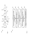
- FIG. 1 depicts a schematic diagram of a chemical sensor in accordance with an illustrative embodiment of the present invention.
- FIG. 2 depicts a method for sensing a target chemical in accordance with the illustrative embodiment of the present invention.
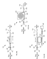
- FIG. 3 depicts a sensing region in accordance with the illustrative embodiment of the present invention.
- FIG. 4A depicts a cross-sectional view of an attenuation region in accordance with the illustrative embodiment of the present invention.
- FIG. 4B depicts a top view of an attenuation region in accordance with the illustrative embodiment of the present invention.
- FIG. 4C depicts a top view of an attenuation region in accordance with a first alternative embodiment of the present invention.
- FIG. 4D depicts a top view of an attenuation region in accordance with a second alternative embodiment of the present invention.
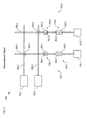
- FIG. 5 depicts a top view of an attenuation region in accordance with a third alternative embodiment of the present invention.
- FIG. 1 depicts a schematic diagram of a chemical sensor in accordance with an illustrative embodiment of the present invention.
- Sensor 100 is a scanning sensor that comprises source 102, sensing region 108, attenuation region 116, and detector 120.
- Sensor 100 provides electrical output signal 122, which is based on the presence of target chemical 110 at sensing region 108.
- FIG. 2 depicts a method for sensing a target chemical in accordance with the illustrative embodiment of the present invention.
- FIG. 2 is described with continuing reference to FIG. 1 .
- Method 200 begins with operation 201, wherein source 102 provides light signal 104 to sensing region 108.
- Light signal 104 comprises stimulative light 106.
- Source 102 is a narrow linewidth light source that provides light signal 104.
- Light signal 104 comprises stimulative light 106, which is substantially coherent light characterized by a wavelength suitable for enabling fluorescence in sensing region 108 ( i . e ., an excitation wavelength for fluorescent material 302, described below and with respect to FIG. 3 ).
- source 102 is other than a monochromatic light source, such as a light emitting diode (LED), mercury lamp, and the like.
- LED light emitting diode
- source 102 must merely provide light suitable for stimulating the material included in sensing region 108. It will be clear to one skilled in the art, after reading this specification, how to specify, make, and use source 102.
- FIG. 3 depicts a sensing region in accordance with the illustrative embodiment of the present invention.
- Sensing region 108 is an optical transducer that provides a fluorescence signal based on the presence of target chemical 110.
- Sensing region 108 comprises fluorescent material 302 and waveguide portion 304.
- Fluorescent material 302 is a material that provides fluorescence signal 114 by fluorescing at a fluorescence wavelength when exposed to both target chemical 110 and stimulative light 106.
- stimulative light 106 is characterized by a wavelength of 650 nanometers (nm)
- fluorescence signal 114 is characterized by a wavelength of 680 nm.
- These wavelengths are merely representative, however, and one skilled in the art will recognize that fluorescent material 302 can be selected from a wide range of fluorescent materials having excitation wavelengths and/or fluorescence wavelengths other than 650 nm and 680 nm, respectively. It will be clear to one skilled in the art, after reading this specification, how to specify, make, and use fluorescent material 302.
- Waveguide portion 304 is a portion of a planar lightwave circuit that comprises surface waveguide 306.
- Surface waveguide 306 is suitable for conveying stimulative light 106 and fluorescence signal 114.
- Surface waveguide 306 comprises lower cladding 308, core 320, and upper cladding 322.
- Surface waveguide 306 has a channel waveguide structure, wherein core 320 is silicon nitride and claddings 308 and 322 are silicon dioxide. The thickness of upper cladding 322 is sufficient to ensure that the evanescent field of stimulative light 106 and fluorescence signal 114 is completely contained within upper cladding 322.
- waveguide 306 has a waveguide structure other than a channel waveguide structure.
- the waveguide structure of waveguide 306 can be any suitable waveguide structure, such as a ridge waveguide, planar waveguide, composite-core waveguide, and the like.
- the use of a composite-core waveguide affords particular advantage to the present invention as the thickness of the upper cladding layer in such a waveguide is typically thin as compared to other waveguide structures. As a result, it can be easier to format sensing and attenuation regions in its upper cladding.
- Composite-core waveguides suitable for use with the present invention are described in U.S. Patent 7,146,087, issued Dec. 5, 2006 (Attorney Docket: 145-001US), which is included herein by reference.
- materials suitable for use in core 320 and claddings 308 and 322 are not limited to silicon nitride and silicon dioxide. In some embodiments, therefore, materials used in core 320 and claddings 308 and 322 include, without limitation, silicon, glasses, silicon nitride, silicon oxides, III-V materials, II-VI materials, germanium, lithium niobate, polymers, and the like.
- the thickness of upper cladding 322 is reduced to thickness, t1 , to facilitate the optically coupling of waveguide portion 304 and material 302.
- light signal 204 is evanescently coupled with fluorescent material 108.
- upper cladding 322 is removed completely in waveguide portion 304.
- Fluorescent material 302 and waveguide portion 304 are optically coupled such that some of the stimulative light propagating in waveguide portion 304 is absorbed by fluorescent material 302. In some embodiments, energy in the evanescent field of the light propagating through the waveguide couples with, and is absorbed by, the fluorescent material.
- source 102 is optically coupled directly with sensing region 108. In some embodiments, source 102 is optically coupled with a different waveguide that is optically coupled with waveguide 306. It will be clear to one skilled in the art, after reading this specification, how to couple light from source 102 into waveguide 306.
- sensing region 108 is exposed to the target chemical 110.
- fluorescent material 108 emits energy gained from the absorption of some of the light in stimulative light 106 as fluorescence signal 114 , which couples into waveguide 306.
- FIGS. 4A and 4B depict a cross-sectional view and top view, respectively, of an attenuation region in accordance with the illustrative embodiment of the present invention.
- Attenuation region 118 comprises wavelength-selective absorbing dye 402 and waveguide portion 404.
- Wavelength-selective absorbing dyes are well-known in the prior art. For example, dyes characterized by narrow absorption-bands have been used in prior-art laser systems as selective wavelength filters.
- Wavelength-selective absorbing dye 402 (hereafter referred to as "dye 402") is more absorptive for light characterized by the excitation wavelength (i.e., stimulative signal 106) than for light characterized by the fluorescence wavelength ( i . e ., fluorescent signal 114).
- Dye 402 is disposed above core 410 in waveguide portion 404.
- Waveguide portion 404 is a portion of waveguide 406.
- Waveguide 406 comprises core 410, lower cladding 408, and upper cladding 412.
- Waveguide portion 404 has length L1 .
- upper cladding 412 is thinned to thickness, t2, to facilitate the optical coupling of light signal 112 and dye 402. Since waveguide portion 404 is unshaped ( i . e ., straight), the interaction length for attenuation region 118 is substantially equal to L1 .
- Waveguide 406 is analogous to waveguide 306 described above and with respect to FIG. 3 .
- Wavelength-selective absorbing dye 402 and waveguide portion 404 are optically coupled such that light signal 112 propagating in waveguide portion 404 interacts with wavelength-selective absorbing dye 402.
- Waveguide portion 404 and waveguide portion 304 are optically coupled such that light propagating in waveguide portion 304 is coupled into waveguide portion 404.
- waveguide 306 and waveguide 406 are the same waveguide.
- dye 402 absorbs stimulative light 106 but not fluorescence signal 114.
- stimulative light 106 is substantially removed from light signal 112.
- light signal 112 is passed to detector 120 as light signal 118.
- the amount of attenuation of stimulative light 106 in attenuation region 116 is based on the absorptivity of dye 402 for that wavelength, the degree of optical coupling between dye 402 and light signal 112, and the interaction length of attenuation region 116.
- stimulative light 106 is not completely removed from signal 112 at attenuation region 116.
- some attenuation of fluorescence signal 114 also occurs at attenuation region 116; however, in such embodiments, stimulative light 106 is attenuated more than fluorescence signal 114 so that the signal-to-noise ratio (SNR) of light signal 118 is higher than the SNR of light signal 112.
- SNR signal-to-noise ratio
- detector 120 provides electrical output signal 122 based on received light signal 118 from attenuation region 116.
- the sensitivity of sensor 100 is based on the ability to discriminate changes in the intensity of light signal 118 as received by a photodetector.
- Stimulative light 106 represents noise in light signal 118.
- the present invention therefore, enables an output signal with higher SNR, and higher sensitivity, than chemical sensors in the prior art.
- FIG. 4C depicts a top view of an attenuation region in accordance with a first alternative embodiment of the present invention.
- Attenuation region 414 comprises dye 402 and waveguide portion 416.
- Dye 402 and waveguide portion 416 are optically coupled such that light signal 112 propagating in waveguide portion 416 interacts with wavelength-selective absorbing dye 402.
- Waveguide portion 416 is a shaped waveguide portion that has a spiral shape.
- a "shaped waveguide portion” is defined as a waveguide portion that has a shape other than a substantially straight line.
- the interaction length between dye 402 and waveguide portion 416 can be increased.
- the interaction length of attenuation region 414 is equal to the total length of the spiral-shaped waveguide portion 416 from P1 to P2. As a result, a higher attenuation of stimulative light 106 can be achieved within a reasonable footprint.
- waveguide portion 416 comprises a spiral shape
- waveguide portion 416 comprises a shaped waveguide portion that has a shape other than spiral.
- Suitable shaped waveguide portions include, without limitation, spirals, curves, ovals, and irregular shapes.
- FIG. 4D depicts a top view of an attenuation region in accordance with a second alternative embodiment of the present invention.
- Attenuation region 418 comprises waveguide portion 404, resonant element 420, waveguide portion 422, and beam dump 426.
- Resonant element 420 is an optical resonator that has an optical resonance at the wavelength of stimulative light 106.
- resonant element 420 is a racetrack ring resonator; however, it will be clear to one skilled in the art, after reading this specification, that resonant element 420 can comprise any optical resonant device.
- Resonant element suitable for use in the present invention include, without limitation, disc resonators, ring resonators, tunable resonators, whispering gallery mode resonators, and the like.
- Resonant element 420 and waveguide portion 404 are in close proximity over interaction length L3.
- stimulative light 106 evanescently couples into resonant element 420 as light signal 112 propagates through waveguide portion 404 of waveguide 406.
- at least some of stimulative light 106 is selectively removed from the light signal.
- stimulative light 106 is attenuated at attenuation region 418 such that the intensity of stimulative light 106 in light signal 118 is less than its intensity in light signal 112.
- stimulative light 106 is completely removed from the light signal thereby leaving light signal 118 with only fluorescence signal 114.
- Beam dump 426 receives the stimulative light 106 that has been coupled into waveguide 424, which comprises waveguide portion 422. Beam dump 426 facilitates the removal of the energy of stimulative light 106 from the sensor.
- FIG. 5 depicts a top view of an attenuation region in accordance with a third alternative embodiment of the present invention.
- Sensor 500 comprises two substantially independent chemical sensors 100-1 and 100-2, each of which senses a different target chemical.
- Sensor 100-1 comprises input waveguide 502-1 waveguide 306-1, sensing region 108-1, attenuation region 116-1, and detector 120-1.
- sensor 100-2 comprises input waveguide 502-2 waveguide 306-2, sensing region 108-2, attenuation region 116-2, and detector 120-2.
- Each of sources 102-1 and 102-2 provides substantially monochromatic light characterized by an excitation wavelength suitable for sensing regions 108-1 and 108-2, respectively.
- sensing regions 108 are stimulated by light having the same wavelength; therefore, sources 102-1 and 102-2 provide light at the same wavelength.
- sources 102-1 and 102-2 comprise power couplers that couple light from a single light source into input waveguides 502-1 and 502-2.
- Input waveguide 502-1 is optically coupled with waveguide 306-1 at coupler 504-1. As a result, at least a portion of the light conveyed by input waveguide 502-1 is coupled into waveguide 306-1. In similar fashion, input waveguide 502-2 is optically coupled with waveguide 306-2 at coupler 504-2.
- the third alternative embodiment comprises couplers for coupling waveguides that are oriented orthogonally to one another
- couplers for coupling waveguides that are oriented orthogonally to one another
- alternative embodiments of the present invention that comprise couplers for coupling waveguides that are oriented with one another in any suitable arrangement.
- a sensing region 108 can be co-located with a coupler 504.
- a plurality of sensors 100 is distributed in a two-dimensional arrangement to provide a two-dimensional arrangement of sensing regions 108 that sense the same target chemical.
- the collective outputs of the plurality of sensors can be used to develop a two-dimensional map of the distribution of a target chemical across an area.
- the plurality of sensors is monolithically integrated on a single substrate, the collective outputs of the plurality of sensors can provide a two-dimensional map of a target chemical across the substrate.
Landscapes
- Chemical & Material Sciences (AREA)
- Physics & Mathematics (AREA)
- Health & Medical Sciences (AREA)
- Immunology (AREA)
- Pathology (AREA)
- Life Sciences & Earth Sciences (AREA)
- Analytical Chemistry (AREA)
- Biochemistry (AREA)
- General Health & Medical Sciences (AREA)
- General Physics & Mathematics (AREA)
- Chemical Kinetics & Catalysis (AREA)
- Plasma & Fusion (AREA)
- Engineering & Computer Science (AREA)
- Optics & Photonics (AREA)
- Nuclear Medicine, Radiotherapy & Molecular Imaging (AREA)
- Investigating, Analyzing Materials By Fluorescence Or Luminescence (AREA)
Applications Claiming Priority (1)
| Application Number | Priority Date | Filing Date | Title |
|---|---|---|---|
| US12/554,721 US8154716B2 (en) | 2009-09-04 | 2009-09-04 | Waveguide-based sensor |
Publications (3)
| Publication Number | Publication Date |
|---|---|
| EP2293045A2 true EP2293045A2 (fr) | 2011-03-09 |
| EP2293045A3 EP2293045A3 (fr) | 2011-11-23 |
| EP2293045B1 EP2293045B1 (fr) | 2018-05-02 |
Family
ID=43216477
Family Applications (1)
| Application Number | Title | Priority Date | Filing Date |
|---|---|---|---|
| EP10175086.7A Active EP2293045B1 (fr) | 2009-09-04 | 2010-09-02 | Capteur à base de guide d'ondes |
Country Status (2)
| Country | Link |
|---|---|
| US (2) | US8154716B2 (fr) |
| EP (1) | EP2293045B1 (fr) |
Families Citing this family (4)
| Publication number | Priority date | Publication date | Assignee | Title |
|---|---|---|---|---|
| US11754488B2 (en) * | 2009-12-11 | 2023-09-12 | Washington University | Opto-mechanical system and method having chaos induced stochastic resonance and opto-mechanically mediated chaos transfer |
| US10367333B2 (en) * | 2017-04-13 | 2019-07-30 | Nokia Of America Corporation | Increasing fabry-perot cavity free spectral range in hybrid lasers |
| US11125944B2 (en) * | 2020-01-14 | 2021-09-21 | Globalfoundries U.S. Inc. | Polarizer with multiple evanescently coupled waveguides |
| US12320682B2 (en) | 2023-06-23 | 2025-06-03 | Washington University | High-Q whispering gallery mode (WGM) resonators encapsulated in polydimethylsilozane (PDMS) for highly sensitive displacement detection |
Citations (1)
| Publication number | Priority date | Publication date | Assignee | Title |
|---|---|---|---|---|
| US7146087B2 (en) | 2004-01-13 | 2006-12-05 | Lionix Bv | Low modal birefringent waveguides and method of fabrication |
Family Cites Families (11)
| Publication number | Priority date | Publication date | Assignee | Title |
|---|---|---|---|---|
| US5262638A (en) | 1991-09-16 | 1993-11-16 | The United States Of America As Represented By The United States National Aeronautics And Space Administration | Optical fibers and fluorosensors having improved power efficiency and methods of producing same |
| MXPA96005828A (es) * | 1994-05-27 | 2005-07-15 | Novartis Ag Tambien Denominada | Proceso para detectar luminescencia excitada evanescentemente. |
| US5809185A (en) | 1996-04-26 | 1998-09-15 | Mitchell; Ralph | Sensor for detecting microorganisms |
| US6103535A (en) | 1996-05-31 | 2000-08-15 | University Of Maryland | Optical fiber evanescent field excited fluorosensor and method of manufacture |
| KR100269173B1 (ko) * | 1997-09-12 | 2000-10-16 | 윤종용 | 손실흡수를위한광도파로소자및그제작방법 |
| EP2275802A1 (fr) * | 2000-08-09 | 2011-01-19 | Artificial Sensing Instruments ASI AG | Structure de grille conductrice d'ondes et agencement de mesure optique |
| GB0122546D0 (en) * | 2001-09-19 | 2001-11-07 | Univ Cranfield | Optical fibre long period grating with thin film overlays |
| CA2372637A1 (fr) | 2002-02-20 | 2003-08-20 | Institut National D'optique | Capteurs optiques integres au cote de fibres optiques |
| WO2005019798A2 (fr) * | 2003-08-13 | 2005-03-03 | The Regents Of The University Of Michigan | Capteurs biochimiques a micro-resonateurs |
| US7835608B2 (en) * | 2006-03-21 | 2010-11-16 | Lockheed Martin Corporation | Method and apparatus for optical delivery fiber having cladding with absorbing regions |
| US20100047919A1 (en) * | 2006-11-10 | 2010-02-25 | Koninklijke Philips Electronics N.V. | Biosensor device and method for detecting molecules in an analyte |
-
2009
- 2009-09-04 US US12/554,721 patent/US8154716B2/en active Active
-
2010
- 2010-09-02 EP EP10175086.7A patent/EP2293045B1/fr active Active
-
2012
- 2012-01-31 US US13/363,031 patent/US8253933B2/en active Active
Patent Citations (1)
| Publication number | Priority date | Publication date | Assignee | Title |
|---|---|---|---|---|
| US7146087B2 (en) | 2004-01-13 | 2006-12-05 | Lionix Bv | Low modal birefringent waveguides and method of fabrication |
Also Published As
| Publication number | Publication date |
|---|---|
| US8253933B2 (en) | 2012-08-28 |
| US8154716B2 (en) | 2012-04-10 |
| US20120181451A1 (en) | 2012-07-19 |
| EP2293045A3 (fr) | 2011-11-23 |
| US20110058158A1 (en) | 2011-03-10 |
| EP2293045B1 (fr) | 2018-05-02 |
Similar Documents
| Publication | Publication Date | Title |
|---|---|---|
| US8254733B2 (en) | Optical chemical detector and method | |
| US6483096B1 (en) | Integrated-optical chemical and biochemical sensor | |
| US20120012739A1 (en) | Optical microresonator system | |
| US20080291446A1 (en) | Optical sensing device | |
| EP1923693A1 (fr) | Appareil et procédé de détection chimique et biologique | |
| JPH0921698A (ja) | 光学的センサー | |
| US6661938B2 (en) | Optical micro-cavity sensors | |
| EP3492909B1 (fr) | Dispositif de détection chimique utilisant un matériau de détection fluorescent | |
| US8253933B2 (en) | Waveguide-based sensor | |
| EP2053385A2 (fr) | Appareil et procédé pour détecter la présence d'un agent | |
| US9146235B2 (en) | Integrated fluorescence detection | |
| US7952772B2 (en) | Photonic crystal fiber sensor | |
| EP3559638B1 (fr) | Dispositif de collecte de lumière fluorescente émise par des particules dans un milieu | |
| JP7793993B2 (ja) | 光センシング回路及び光センシング方法 | |
| JP4565061B2 (ja) | 光分岐回路及びセンサ | |
| JP2024084468A (ja) | 光センシング回路及び光センシングシステム | |
| Onawa et al. | Wavelength Division Multiplexing Multi-Channel Sensing Circuit Using Si on Insulator Platform | |
| JP2025515831A5 (fr) | ||
| JP2011033623A (ja) | フォトニック結晶ファイバセンサ | |
| Reck et al. | Si3N4 Microring-Resonator-Based Integrated Photonic Sensor for Enhanced Label-Free Biofluid Analysis in the 850 nm Optical Band | |
| CA3044733C (fr) | Dispositif de collecte de lumiere fluorescente emise par des particules dans un milieu | |
| Lambeck et al. | Planar waveguiding systems for optical sensing |
Legal Events
| Date | Code | Title | Description |
|---|---|---|---|
| PUAI | Public reference made under article 153(3) epc to a published international application that has entered the european phase |
Free format text: ORIGINAL CODE: 0009012 |
|
| 17P | Request for examination filed |
Effective date: 20100902 |
|
| AK | Designated contracting states |
Kind code of ref document: A2 Designated state(s): AL AT BE BG CH CY CZ DE DK EE ES FI FR GB GR HR HU IE IS IT LI LT LU LV MC MK MT NL NO PL PT RO SE SI SK SM TR |
|
| AX | Request for extension of the european patent |
Extension state: BA ME RS |
|
| PUAL | Search report despatched |
Free format text: ORIGINAL CODE: 0009013 |
|
| AK | Designated contracting states |
Kind code of ref document: A3 Designated state(s): AL AT BE BG CH CY CZ DE DK EE ES FI FR GB GR HR HU IE IS IT LI LT LU LV MC MK MT NL NO PL PT RO SE SI SK SM TR |
|
| AX | Request for extension of the european patent |
Extension state: BA ME RS |
|
| RIC1 | Information provided on ipc code assigned before grant |
Ipc: G01N 21/64 20060101AFI20111019BHEP Ipc: G01N 21/77 20060101ALI20111019BHEP |
|
| 17Q | First examination report despatched |
Effective date: 20160708 |
|
| STAA | Information on the status of an ep patent application or granted ep patent |
Free format text: STATUS: EXAMINATION IS IN PROGRESS |
|
| GRAP | Despatch of communication of intention to grant a patent |
Free format text: ORIGINAL CODE: EPIDOSNIGR1 |
|
| STAA | Information on the status of an ep patent application or granted ep patent |
Free format text: STATUS: GRANT OF PATENT IS INTENDED |
|
| INTG | Intention to grant announced |
Effective date: 20171106 |
|
| RAP1 | Party data changed (applicant data changed or rights of an application transferred) |
Owner name: LIONIX INTERNATIONAL B.V. |
|
| GRAS | Grant fee paid |
Free format text: ORIGINAL CODE: EPIDOSNIGR3 |
|
| GRAA | (expected) grant |
Free format text: ORIGINAL CODE: 0009210 |
|
| STAA | Information on the status of an ep patent application or granted ep patent |
Free format text: STATUS: THE PATENT HAS BEEN GRANTED |
|
| AK | Designated contracting states |
Kind code of ref document: B1 Designated state(s): AL AT BE BG CH CY CZ DE DK EE ES FI FR GB GR HR HU IE IS IT LI LT LU LV MC MK MT NL NO PL PT RO SE SI SK SM TR |
|
| REG | Reference to a national code |
Ref country code: GB Ref legal event code: FG4D |
|
| REG | Reference to a national code |
Ref country code: CH Ref legal event code: EP Ref country code: AT Ref legal event code: REF Ref document number: 995805 Country of ref document: AT Kind code of ref document: T Effective date: 20180515 |
|
| REG | Reference to a national code |
Ref country code: DE Ref legal event code: R096 Ref document number: 602010050322 Country of ref document: DE Ref country code: IE Ref legal event code: FG4D |
|
| REG | Reference to a national code |
Ref country code: NL Ref legal event code: FP |
|
| REG | Reference to a national code |
Ref country code: LT Ref legal event code: MG4D |
|
| REG | Reference to a national code |
Ref country code: FR Ref legal event code: PLFP Year of fee payment: 9 |
|
| PG25 | Lapsed in a contracting state [announced via postgrant information from national office to epo] |
Ref country code: SE Free format text: LAPSE BECAUSE OF FAILURE TO SUBMIT A TRANSLATION OF THE DESCRIPTION OR TO PAY THE FEE WITHIN THE PRESCRIBED TIME-LIMIT Effective date: 20180502 Ref country code: LT Free format text: LAPSE BECAUSE OF FAILURE TO SUBMIT A TRANSLATION OF THE DESCRIPTION OR TO PAY THE FEE WITHIN THE PRESCRIBED TIME-LIMIT Effective date: 20180502 Ref country code: FI Free format text: LAPSE BECAUSE OF FAILURE TO SUBMIT A TRANSLATION OF THE DESCRIPTION OR TO PAY THE FEE WITHIN THE PRESCRIBED TIME-LIMIT Effective date: 20180502 Ref country code: BG Free format text: LAPSE BECAUSE OF FAILURE TO SUBMIT A TRANSLATION OF THE DESCRIPTION OR TO PAY THE FEE WITHIN THE PRESCRIBED TIME-LIMIT Effective date: 20180802 Ref country code: ES Free format text: LAPSE BECAUSE OF FAILURE TO SUBMIT A TRANSLATION OF THE DESCRIPTION OR TO PAY THE FEE WITHIN THE PRESCRIBED TIME-LIMIT Effective date: 20180502 Ref country code: NO Free format text: LAPSE BECAUSE OF FAILURE TO SUBMIT A TRANSLATION OF THE DESCRIPTION OR TO PAY THE FEE WITHIN THE PRESCRIBED TIME-LIMIT Effective date: 20180802 |
|
| PG25 | Lapsed in a contracting state [announced via postgrant information from national office to epo] |
Ref country code: LV Free format text: LAPSE BECAUSE OF FAILURE TO SUBMIT A TRANSLATION OF THE DESCRIPTION OR TO PAY THE FEE WITHIN THE PRESCRIBED TIME-LIMIT Effective date: 20180502 Ref country code: HR Free format text: LAPSE BECAUSE OF FAILURE TO SUBMIT A TRANSLATION OF THE DESCRIPTION OR TO PAY THE FEE WITHIN THE PRESCRIBED TIME-LIMIT Effective date: 20180502 Ref country code: GR Free format text: LAPSE BECAUSE OF FAILURE TO SUBMIT A TRANSLATION OF THE DESCRIPTION OR TO PAY THE FEE WITHIN THE PRESCRIBED TIME-LIMIT Effective date: 20180803 |
|
| REG | Reference to a national code |
Ref country code: AT Ref legal event code: MK05 Ref document number: 995805 Country of ref document: AT Kind code of ref document: T Effective date: 20180502 |
|
| PG25 | Lapsed in a contracting state [announced via postgrant information from national office to epo] |
Ref country code: PT Free format text: LAPSE BECAUSE OF FAILURE TO SUBMIT A TRANSLATION OF THE DESCRIPTION OR TO PAY THE FEE WITHIN THE PRESCRIBED TIME-LIMIT Effective date: 20180903 |
|
| PG25 | Lapsed in a contracting state [announced via postgrant information from national office to epo] |
Ref country code: AT Free format text: LAPSE BECAUSE OF FAILURE TO SUBMIT A TRANSLATION OF THE DESCRIPTION OR TO PAY THE FEE WITHIN THE PRESCRIBED TIME-LIMIT Effective date: 20180502 Ref country code: PL Free format text: LAPSE BECAUSE OF FAILURE TO SUBMIT A TRANSLATION OF THE DESCRIPTION OR TO PAY THE FEE WITHIN THE PRESCRIBED TIME-LIMIT Effective date: 20180502 Ref country code: CZ Free format text: LAPSE BECAUSE OF FAILURE TO SUBMIT A TRANSLATION OF THE DESCRIPTION OR TO PAY THE FEE WITHIN THE PRESCRIBED TIME-LIMIT Effective date: 20180502 Ref country code: SK Free format text: LAPSE BECAUSE OF FAILURE TO SUBMIT A TRANSLATION OF THE DESCRIPTION OR TO PAY THE FEE WITHIN THE PRESCRIBED TIME-LIMIT Effective date: 20180502 Ref country code: RO Free format text: LAPSE BECAUSE OF FAILURE TO SUBMIT A TRANSLATION OF THE DESCRIPTION OR TO PAY THE FEE WITHIN THE PRESCRIBED TIME-LIMIT Effective date: 20180502 Ref country code: EE Free format text: LAPSE BECAUSE OF FAILURE TO SUBMIT A TRANSLATION OF THE DESCRIPTION OR TO PAY THE FEE WITHIN THE PRESCRIBED TIME-LIMIT Effective date: 20180502 Ref country code: DK Free format text: LAPSE BECAUSE OF FAILURE TO SUBMIT A TRANSLATION OF THE DESCRIPTION OR TO PAY THE FEE WITHIN THE PRESCRIBED TIME-LIMIT Effective date: 20180502 |
|
| REG | Reference to a national code |
Ref country code: DE Ref legal event code: R097 Ref document number: 602010050322 Country of ref document: DE |
|
| PG25 | Lapsed in a contracting state [announced via postgrant information from national office to epo] |
Ref country code: IT Free format text: LAPSE BECAUSE OF FAILURE TO SUBMIT A TRANSLATION OF THE DESCRIPTION OR TO PAY THE FEE WITHIN THE PRESCRIBED TIME-LIMIT Effective date: 20180502 Ref country code: SM Free format text: LAPSE BECAUSE OF FAILURE TO SUBMIT A TRANSLATION OF THE DESCRIPTION OR TO PAY THE FEE WITHIN THE PRESCRIBED TIME-LIMIT Effective date: 20180502 |
|
| PLBE | No opposition filed within time limit |
Free format text: ORIGINAL CODE: 0009261 |
|
| STAA | Information on the status of an ep patent application or granted ep patent |
Free format text: STATUS: NO OPPOSITION FILED WITHIN TIME LIMIT |
|
| 26N | No opposition filed |
Effective date: 20190205 |
|
| PG25 | Lapsed in a contracting state [announced via postgrant information from national office to epo] |
Ref country code: MC Free format text: LAPSE BECAUSE OF FAILURE TO SUBMIT A TRANSLATION OF THE DESCRIPTION OR TO PAY THE FEE WITHIN THE PRESCRIBED TIME-LIMIT Effective date: 20180502 |
|
| REG | Reference to a national code |
Ref country code: CH Ref legal event code: PL |
|
| PG25 | Lapsed in a contracting state [announced via postgrant information from national office to epo] |
Ref country code: SI Free format text: LAPSE BECAUSE OF FAILURE TO SUBMIT A TRANSLATION OF THE DESCRIPTION OR TO PAY THE FEE WITHIN THE PRESCRIBED TIME-LIMIT Effective date: 20180502 |
|
| REG | Reference to a national code |
Ref country code: IE Ref legal event code: MM4A |
|
| PG25 | Lapsed in a contracting state [announced via postgrant information from national office to epo] |
Ref country code: LU Free format text: LAPSE BECAUSE OF NON-PAYMENT OF DUE FEES Effective date: 20180902 |
|
| PG25 | Lapsed in a contracting state [announced via postgrant information from national office to epo] |
Ref country code: IE Free format text: LAPSE BECAUSE OF NON-PAYMENT OF DUE FEES Effective date: 20180902 |
|
| PG25 | Lapsed in a contracting state [announced via postgrant information from national office to epo] |
Ref country code: LI Free format text: LAPSE BECAUSE OF NON-PAYMENT OF DUE FEES Effective date: 20180930 Ref country code: CH Free format text: LAPSE BECAUSE OF NON-PAYMENT OF DUE FEES Effective date: 20180930 |
|
| PG25 | Lapsed in a contracting state [announced via postgrant information from national office to epo] |
Ref country code: AL Free format text: LAPSE BECAUSE OF FAILURE TO SUBMIT A TRANSLATION OF THE DESCRIPTION OR TO PAY THE FEE WITHIN THE PRESCRIBED TIME-LIMIT Effective date: 20180502 |
|
| PG25 | Lapsed in a contracting state [announced via postgrant information from national office to epo] |
Ref country code: MT Free format text: LAPSE BECAUSE OF NON-PAYMENT OF DUE FEES Effective date: 20180902 |
|
| PG25 | Lapsed in a contracting state [announced via postgrant information from national office to epo] |
Ref country code: TR Free format text: LAPSE BECAUSE OF FAILURE TO SUBMIT A TRANSLATION OF THE DESCRIPTION OR TO PAY THE FEE WITHIN THE PRESCRIBED TIME-LIMIT Effective date: 20180502 |
|
| PG25 | Lapsed in a contracting state [announced via postgrant information from national office to epo] |
Ref country code: HU Free format text: LAPSE BECAUSE OF FAILURE TO SUBMIT A TRANSLATION OF THE DESCRIPTION OR TO PAY THE FEE WITHIN THE PRESCRIBED TIME-LIMIT; INVALID AB INITIO Effective date: 20100902 |
|
| PG25 | Lapsed in a contracting state [announced via postgrant information from national office to epo] |
Ref country code: CY Free format text: LAPSE BECAUSE OF FAILURE TO SUBMIT A TRANSLATION OF THE DESCRIPTION OR TO PAY THE FEE WITHIN THE PRESCRIBED TIME-LIMIT Effective date: 20180502 Ref country code: MK Free format text: LAPSE BECAUSE OF NON-PAYMENT OF DUE FEES Effective date: 20180502 |
|
| PG25 | Lapsed in a contracting state [announced via postgrant information from national office to epo] |
Ref country code: IS Free format text: LAPSE BECAUSE OF FAILURE TO SUBMIT A TRANSLATION OF THE DESCRIPTION OR TO PAY THE FEE WITHIN THE PRESCRIBED TIME-LIMIT Effective date: 20180902 |
|
| REG | Reference to a national code |
Ref country code: NL Ref legal event code: RC Free format text: DETAILS LICENCE OR PLEDGE: RIGHT OF PLEDGE, ESTABLISHED Name of requester: ONTWIKKELINGSMAATSCHAPPIJ OOST-NEDERLAND N.V. Effective date: 20250204 |
|
| REG | Reference to a national code |
Ref country code: BE Ref legal event code: RC Free format text: DETAILS PLEDGE: RIGHT OF PLEDGE, ESTABLISHED Name of requester: ONTWIKKELINGSMAATSCHAPPIJ OOST-NEDERLAND N.V. Effective date: 20250210 Ref country code: BE Ref legal event code: PD Owner name: LIONIX INTERNATIONAL BV; NL Free format text: DETAILS ASSIGNMENT: CHANGE OF OWNER(S), OTHER; FORMER OWNER NAME: LIONIX INTERNATIONAL B.V. Effective date: 20250210 |
|
| PGFP | Annual fee paid to national office [announced via postgrant information from national office to epo] |
Ref country code: DE Payment date: 20250929 Year of fee payment: 16 |
|
| PGFP | Annual fee paid to national office [announced via postgrant information from national office to epo] |
Ref country code: NL Payment date: 20250926 Year of fee payment: 16 |
|
| PGFP | Annual fee paid to national office [announced via postgrant information from national office to epo] |
Ref country code: GB Payment date: 20250929 Year of fee payment: 16 Ref country code: BE Payment date: 20250929 Year of fee payment: 16 |
|
| PGFP | Annual fee paid to national office [announced via postgrant information from national office to epo] |
Ref country code: FR Payment date: 20250925 Year of fee payment: 16 |
|
| REG | Reference to a national code |
Ref country code: DE Ref legal event code: R082 Ref document number: 602010050322 Country of ref document: DE Representative=s name: WESTPHAL, MUSSGNUG & PARTNER PATENTANWAELTE MI, DE |