EP2293325B1 - Elektronische Halbleitervorrichtung und Verfahren zu deren Herstellung - Google Patents
Elektronische Halbleitervorrichtung und Verfahren zu deren Herstellung Download PDFInfo
- Publication number
- EP2293325B1 EP2293325B1 EP10183262.4A EP10183262A EP2293325B1 EP 2293325 B1 EP2293325 B1 EP 2293325B1 EP 10183262 A EP10183262 A EP 10183262A EP 2293325 B1 EP2293325 B1 EP 2293325B1
- Authority
- EP
- European Patent Office
- Prior art keywords
- film
- alloys
- electronic device
- gold
- die
- Prior art date
- Legal status (The legal status is an assumption and is not a legal conclusion. Google has not performed a legal analysis and makes no representation as to the accuracy of the status listed.)
- Expired - Lifetime
Links
Images
Classifications
-
- H—ELECTRICITY
- H10—SEMICONDUCTOR DEVICES; ELECTRIC SOLID-STATE DEVICES NOT OTHERWISE PROVIDED FOR
- H10W—GENERIC PACKAGES, INTERCONNECTIONS, CONNECTORS OR OTHER CONSTRUCTIONAL DETAILS OF DEVICES COVERED BY CLASS H10
- H10W20/00—Interconnections in chips, wafers or substrates
- H10W20/40—Interconnections external to wafers or substrates, e.g. back-end-of-line [BEOL] metallisations or vias connecting to gate electrodes
- H10W20/41—Interconnections external to wafers or substrates, e.g. back-end-of-line [BEOL] metallisations or vias connecting to gate electrodes characterised by their conductive parts
- H10W20/425—Barrier, adhesion or liner layers
-
- H—ELECTRICITY
- H10—SEMICONDUCTOR DEVICES; ELECTRIC SOLID-STATE DEVICES NOT OTHERWISE PROVIDED FOR
- H10W—GENERIC PACKAGES, INTERCONNECTIONS, CONNECTORS OR OTHER CONSTRUCTIONAL DETAILS OF DEVICES COVERED BY CLASS H10
- H10W72/00—Interconnections or connectors in packages
- H10W72/01—Manufacture or treatment
- H10W72/019—Manufacture or treatment of bond pads
-
- H—ELECTRICITY
- H10—SEMICONDUCTOR DEVICES; ELECTRIC SOLID-STATE DEVICES NOT OTHERWISE PROVIDED FOR
- H10W—GENERIC PACKAGES, INTERCONNECTIONS, CONNECTORS OR OTHER CONSTRUCTIONAL DETAILS OF DEVICES COVERED BY CLASS H10
- H10W72/00—Interconnections or connectors in packages
- H10W72/071—Connecting or disconnecting
- H10W72/075—Connecting or disconnecting of bond wires
- H10W72/07531—Techniques
- H10W72/07532—Compression bonding, e.g. thermocompression bonding
- H10W72/07533—Ultrasonic bonding, e.g. thermosonic bonding
-
- H—ELECTRICITY
- H10—SEMICONDUCTOR DEVICES; ELECTRIC SOLID-STATE DEVICES NOT OTHERWISE PROVIDED FOR
- H10W—GENERIC PACKAGES, INTERCONNECTIONS, CONNECTORS OR OTHER CONSTRUCTIONAL DETAILS OF DEVICES COVERED BY CLASS H10
- H10W72/00—Interconnections or connectors in packages
- H10W72/50—Bond wires
- H10W72/531—Shapes of wire connectors
- H10W72/536—Shapes of wire connectors the connected ends being ball-shaped
-
- H—ELECTRICITY
- H10—SEMICONDUCTOR DEVICES; ELECTRIC SOLID-STATE DEVICES NOT OTHERWISE PROVIDED FOR
- H10W—GENERIC PACKAGES, INTERCONNECTIONS, CONNECTORS OR OTHER CONSTRUCTIONAL DETAILS OF DEVICES COVERED BY CLASS H10
- H10W72/00—Interconnections or connectors in packages
- H10W72/50—Bond wires
- H10W72/531—Shapes of wire connectors
- H10W72/5363—Shapes of wire connectors the connected ends being wedge-shaped
-
- H—ELECTRICITY
- H10—SEMICONDUCTOR DEVICES; ELECTRIC SOLID-STATE DEVICES NOT OTHERWISE PROVIDED FOR
- H10W—GENERIC PACKAGES, INTERCONNECTIONS, CONNECTORS OR OTHER CONSTRUCTIONAL DETAILS OF DEVICES COVERED BY CLASS H10
- H10W72/00—Interconnections or connectors in packages
- H10W72/50—Bond wires
- H10W72/551—Materials of bond wires
- H10W72/552—Materials of bond wires comprising metals or metalloids, e.g. silver
- H10W72/5522—Materials of bond wires comprising metals or metalloids, e.g. silver comprising gold [Au]
-
- H—ELECTRICITY
- H10—SEMICONDUCTOR DEVICES; ELECTRIC SOLID-STATE DEVICES NOT OTHERWISE PROVIDED FOR
- H10W—GENERIC PACKAGES, INTERCONNECTIONS, CONNECTORS OR OTHER CONSTRUCTIONAL DETAILS OF DEVICES COVERED BY CLASS H10
- H10W72/00—Interconnections or connectors in packages
- H10W72/50—Bond wires
- H10W72/551—Materials of bond wires
- H10W72/552—Materials of bond wires comprising metals or metalloids, e.g. silver
- H10W72/5525—Materials of bond wires comprising metals or metalloids, e.g. silver comprising copper [Cu]
-
- H—ELECTRICITY
- H10—SEMICONDUCTOR DEVICES; ELECTRIC SOLID-STATE DEVICES NOT OTHERWISE PROVIDED FOR
- H10W—GENERIC PACKAGES, INTERCONNECTIONS, CONNECTORS OR OTHER CONSTRUCTIONAL DETAILS OF DEVICES COVERED BY CLASS H10
- H10W72/00—Interconnections or connectors in packages
- H10W72/50—Bond wires
- H10W72/59—Bond pads specially adapted therefor
-
- H—ELECTRICITY
- H10—SEMICONDUCTOR DEVICES; ELECTRIC SOLID-STATE DEVICES NOT OTHERWISE PROVIDED FOR
- H10W—GENERIC PACKAGES, INTERCONNECTIONS, CONNECTORS OR OTHER CONSTRUCTIONAL DETAILS OF DEVICES COVERED BY CLASS H10
- H10W72/00—Interconnections or connectors in packages
- H10W72/90—Bond pads, in general
- H10W72/921—Structures or relative sizes of bond pads
- H10W72/923—Bond pads having multiple stacked layers
-
- H—ELECTRICITY
- H10—SEMICONDUCTOR DEVICES; ELECTRIC SOLID-STATE DEVICES NOT OTHERWISE PROVIDED FOR
- H10W—GENERIC PACKAGES, INTERCONNECTIONS, CONNECTORS OR OTHER CONSTRUCTIONAL DETAILS OF DEVICES COVERED BY CLASS H10
- H10W72/00—Interconnections or connectors in packages
- H10W72/90—Bond pads, in general
- H10W72/951—Materials of bond pads
- H10W72/952—Materials of bond pads comprising metals or metalloids, e.g. PbSn, Ag or Cu
-
- H—ELECTRICITY
- H10—SEMICONDUCTOR DEVICES; ELECTRIC SOLID-STATE DEVICES NOT OTHERWISE PROVIDED FOR
- H10W—GENERIC PACKAGES, INTERCONNECTIONS, CONNECTORS OR OTHER CONSTRUCTIONAL DETAILS OF DEVICES COVERED BY CLASS H10
- H10W90/00—Package configurations
- H10W90/701—Package configurations characterised by the relative positions of pads or connectors relative to package parts
- H10W90/751—Package configurations characterised by the relative positions of pads or connectors relative to package parts of bond wires
- H10W90/754—Package configurations characterised by the relative positions of pads or connectors relative to package parts of bond wires between a chip and a stacked insulating package substrate, interposer or RDL
-
- H—ELECTRICITY
- H10—SEMICONDUCTOR DEVICES; ELECTRIC SOLID-STATE DEVICES NOT OTHERWISE PROVIDED FOR
- H10W—GENERIC PACKAGES, INTERCONNECTIONS, CONNECTORS OR OTHER CONSTRUCTIONAL DETAILS OF DEVICES COVERED BY CLASS H10
- H10W90/00—Package configurations
- H10W90/701—Package configurations characterised by the relative positions of pads or connectors relative to package parts
- H10W90/751—Package configurations characterised by the relative positions of pads or connectors relative to package parts of bond wires
- H10W90/756—Package configurations characterised by the relative positions of pads or connectors relative to package parts of bond wires between a chip and a stacked lead frame, conducting package substrate or heat sink
Definitions
- the present invention broadly relates to an electronic device of a type that comprises a die of semiconductor material connected by wire leads to a support or an integrated circuit having electrically conductive areas or regions.
- the invention relates to an electronic device as above exhibiting high performance and reliability features especially, but not solely, under working conditions of high temperature.
- the invention further relates to a method of fabricating a semiconductor electronic device as above.
- a semiconductor electronic device e.g. a power device
- a semiconductor electronic device comprises a small plate of a semiconductor material known as the "die", which has a surface area of a few square millimetres and has an electronic circuit integrated monolithically therein.
- the die has a plurality of terminals, typically in the form of surface contact pads that are connected electrically to a support being a part of the electronic device.
- This support is known as the "lead frame” and can be provided in different forms, including ceramic substrates, printed circuit boards, pliant circuits, and silicon-based substrates.
- the aggregate of the die and the support is encased into a "package" for heat and mechanical protection of the electronic device, both during storage and in use.
- the package case is typically of a plastics material.
- each wire is soldered with one end on a contact pad formed on the die of semiconductor material, and with the other end on a contact pad correspondingly formed on the support to which the die must be connected.
- the contact pads of a die of semiconductor material are typically made of aluminium or an aluminium alloy, for reasons of manufacturing convenience and performance of the device.
- the wires are usually of gold, copper, or alloys thereof, because these materials alloy well with aluminium.
- semiconductor electronic devices of the above type are advantageous, they have serious drawbacks in that their reliability is low and their performance deteriorate rapidly in high-temperature applications.
- control units are made smaller and smaller in size and include an ever-growing number of functions, which results in increased power density and consequently increased heat generated from the integrated circuits.
- this heat is normally dissipated through their packages, which are designed to also serve this purpose or are provided with suitable heat sinks.
- the packages of power electronic devices utilized in automotive control units are not able to dissipate the heat properly due to the high ambient temperature (usually above 100°C) to which the control units and consequently the semiconductor devices therein must withstand.
- US 6 281 046 discloses a stack of Al/Zn/Ni/Au.
- the zinc layer is applied to the base aluminium as an adhesion layer for the nickel.
- the gold layer is deposited.
- the objective in this document is to protect the underlying aluminium material from oxidation.
- US 5 249 728 concerns a stack of Al/Ti-W/Pd/Au.
- Ti-W acts as an adhesion layer for the palladium layer which, in turn, has a diffusion barrier function.
- the technical problem underlying the present invention is to provide a semiconductor electronic device with appropriate structural and functional features to overcome the aforementioned drawbacks of the prior art and fill the above demand.
- a semiconductor electronic device that comprises a die of semiconductor material and a support, the die of semiconductor material including an integrated electronic circuit and a plurality of contact pads associated with the electronic circuit and connected electrically to the support by wire leads, and is characterized in that each contact pad of said plurality of contact pads comprises:
- each contact pad on the die of semiconductor material is intended for connection to a corresponding contact pad on a support by means of a soldered wire, preferably a wire of gold, copper, or alloys thereof.
- connection of a contact pad to the lead wire can be obtained by soldering the outermost metal film of the upper layer, i.e. the palladium or gold film, to one end of the lead wire.
- the outermost film of the upper layer could be formed on the outermost film of the upper layer, a soldering protuberance or bump, of gold, copper, or alloys thereof, which would be soldered on the outermost film in the upper layer and to one end of the wire.
- nickel and/ or palladium films in the upper layer of the contact pads effectively blocks the migration of metal atoms from the wire lead and its soldering bump, if any, as well as that of gold or gold alloy atoms from the optional outermost film on the contact pads, toward the lower layer of aluminium, copper, or alloys thereof, thereby preventing the formation of highly resistive intermetallic compounds.
- This atom blocking action is also effective when the semiconductor device of this invention is operated at high temperatures and large currents.
- the semiconductor electronic device of this invention is advantageous in that it can be used for power applications, such as automotive control units, and any other applications involving high working temperatures.
- the thickness of the film of nickel, or alloys thereof should be at least 1 micron, preferably 1 to 20 microns, in the semiconductor device of this invention.
- a palladium film is used, alone or in combination with the nickel film, a palladium film 0.1 to 3 microns thick is preferred for an effective blocking action.
- the thickness of the film of gold or gold alloys is preferably comprised from 0.1 micron to 3 micron to guarantee an efficient bonding between the contact pad and the metal wire.
- the film of gold or gold alloy is important when only nickel films are used to guarantee atomic migration blocking action.
- the thickness of the lower layer of aluminium, or alloys thereof is preferably 0.7 to 10 microns. Because nickel films are used, it is important that the lower layer of aluminium, or alloys thereof, be covered with a zinc film having a thickness of 0.05 to 0.3 microns, to assist in depositing the nickel onto said lower layer.
- This invention also relates to a process as claimed in claim 8 for fabricating a semiconductor electronic device comprised of a die of semiconductor material and a support, wherein the die of semiconductor material includes an integrated electronic circuit and a plurality of contact pads associated with the electronic circuit and connected electrically to the support by wire leads.
- the steps of depositing the above-described lower layer and metal films are carried out by electroless deposition.
- This deposition is conventional and comprises the steps of dipping the die in a plating bath containing ions of the metal to be deposited, and of chemically reducing the bath ions to cause a film of the metal to deposit over exposed surface portions of the die, or over the surface of a film or metal layer previously deposited on such exposed surface portions.
- the deposited layer or metal film will overlie an exposed surface portion of the die or a surface of a film or metal layer previously deposited on such exposed surface portions.
- the process may further comprise the step of depositing a soldering bump of gold, copper, or alloys thereof, over the outermost film of the contact pad, namely over the palladium or the gold film.
- the soldering bump is deposited by conventional methods, preferably using thermosonic or ultrasonic energy. According to these methods, the material of the soldering bump is supplied through a capillary duct and soldered on the contact pad by the application of ultrasonic energy in combination with heat.
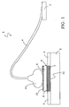
- the device 1 comprises a die 2 of a semiconductor material, which is connected electrically to a support 3 by wire leads 4. Shown in Figure 1 is one wire lead 4 only, for simplicity.
- the die 2 includes an integrated electronic circuit (not shown) and is coated with a layer 5 of an insulating material. This insulating layer 5 has a plurality of openings to expose portions 2a of a surface of the die 2 on which respective contact pads are formed for connecting the die 2 and the support 3 electrically together.
- Figure 1 shows only one portion 2a of the exposed surface of the die 2 where a contact pad is formed as generally shown at 6.
- the contact pad 6 comprises a lower or pad layer 7 of aluminium, or alloys thereof, and an upper layer on top of said lower layer 7.
- the upper layer consists of a first film 8 of zinc completely overlying the lower or pad layer 7 of aluminium, or alloys thereof; a second layer 9 of nickel, or alloys thereof, completely overlying the zinc film 8, and a third film 10 of palladium.
- a fourth film of gold, or alloys thereof, may optionally overly film 10 of palladium.
- Contact pads 6 were formed on a die 2 of semiconductor material, to the following specifications:
- the resulting contact pads 6 were connected electrically into a so-called daisy chain by means of gold wire leads having a diameter of 50.8 microns (2 mils). This produced the semiconductor electronic device of this invention, which was then encased to obtain a 25-pin package.
- the reliability of the electronic device was tested by measuring the resistance increase (deltaR/R) with time of the daisy chain at a setting temperature of 180°C and an electric current of 2.5 A.
- the reliability of the device was compared to that of three conventional electronic devices, each having a die of semiconductor material formed with contact pads to the following specifications:
- Sample 1 The three conventional devices, hereinafter referred to as Sample 1, Sample 2 and Sample 3, differed from one another by the material of their packaging cases.
- the packaging process was completed after connecting the contact pads of each sample device into a daisy chain as previously explained.
- the packaging materials of Samples 1, 2, 3 were as follows:
- Samples 1, 2, 3 were tested for reliability by measuring the increase in resistance (deltaR/R) with time of the daisy chain at a setting temperature of 180°C and an electric current of 2.5 A.
- Contact pads 6 were formed on a die 2 of semiconductor material, to the following specifications:
- the resulting contact pads 6 were connected electrically into a so-called daisy chain by means of gold wire leads having a diameter of 50.8 microns (2 mils). This produced the semiconductor electronic device which was then encased to obtain a 25-pin package.
- the electronic device was tested for reliability by the same procedure as in Example 1.
- the device showed to have constant performances and reliability at a temperature of 180°C and current of 2.5 A, for a time longer than 4000 hours.
Landscapes
- Wire Bonding (AREA)
Claims (11)
- Elektronische Halbleitervorrichtung (1) mit einem Chip (2) aus Halbleitermaterial und mit einem Träger (3), wobei der Chip (2) aus Halbleitermaterial eine integrierte elektronische Schaltung und eine Mehrzahl von Kontaktflächen (6) aufweist, die der elektronischen Schaltung zugeordnet sind und mittels Drahtleitungen (4) mit dem Träger (3) elektrisch verbunden sind, wobei jede Kontaktfläche der Mehrzahl von Kontaktflächen (6) eine untere Schicht (7) aus Aluminium oder Legierungen davon sowie eine obere Schicht aufweist,
dadurch gekennzeichnet, dass die obere Schicht besteht aus:einer ersten Lage (8) aus Zink, die über der unteren Schicht (7) aus Aluminium oder Legierungen davon liegt;einer zweiten Lage (9) aus Nickel oder Legierungen davon, die über der erste Lage (8) aus Zink liegt;einer dritten Lage aus Palladium oder Legierungen davon, die über der zweiten Lage (9) aus Nickel oder Legierungen davon liegt, und wahlweiseeiner vierte Lage (10) aus Gold oder Legierungen davon, die über der dritten Lage aus Palladium oder Legierungen davon liegt. - Elektronische Halbleitervorrichtung (1) nach Anspruch 1,
wobei die Dicke der unteren Schicht (7) aus Aluminium oder Legierungen davon 0,7 bis 10 µm beträgt. - Elektronische Halbleitervorrichtung (1) nach Anspruch 1 oder 2,
wobei die Dicke der zweiten Lage (9) aus Nickel oder Legierungen davon 1 bis 20 µm beträgt. - Elektronische Halbleitervorrichtung (1) nach Anspruch 1,
wobei die Dicke der dritten Lage aus Palladium oder Legierungen davon 0,1 bis 3 µm beträgt. - Elektronische Halbleitervorrichtung (1) nach Anspruch 1,
wobei die Dicke der vierte Lage (10) aus Gold oder Legierungen davon 0,1 bis 3 um beträgt. - Elektronische Halbleitervorrichtung (1) nach Anspruch 1,
wobei die Dicke der ersten Lage (8) aus Zink 0,1 bis 3 µm beträgt. - Elektronische Halbleitervorrichtung (1) nach Anspruch 1,
dadurch gekennzeichnet, dass jede Kontaktfläche der Mehrzahl von Kontaktflächen (6) ferner eine auf der oberen Schicht vorgesehene Löterhebung (11) aus Gold oder Legierungen davon aufweist. - Verfahren zum Herstellen einer elektronischen Halbleitervorrichtung (1) mit einem Chip (2) aus Halbleitermaterial und mit einem Träger (3), wobei der Chip (2) aus Halbleitermaterial eine integrierte elektronische Schaltung und eine Mehrzahl von Kontaktflächen (6) aufweist, die der elektronischen Schaltung zugeordnet sind und mittels Drahtleitungen (4) mit dem Träger (3) elektrisch verbunden sind, wobei das Verfahren dadurch gekennzeichnet ist, dass jede Kontaktfläche der Mehrzahl von Kontaktflächen (6) durch folgende Schritte gebildet wird:Aufbringen einer Schicht (7) aus Aluminium oder Legierungen davon auf einen Oberflächenbereich (2a) des Chips (2);Aufbringen einer ersten Lage (8) aus Zink auf die Schicht (7) aus Aluminium oder Legierungen davon;Aufbringen einer zweiten Lage (9) aus Nickel oder Legierungen davon auf die Lage (8) aus Zink;Aufbringen einer dritten Lage aus Palladium oder Legierungen davon, die über der zweiten Lage (9) aus Nickel oder Legierungen davon liegt, und wahlweiseAufbringen einer vierte Lage (10) aus Gold oder Legierungen davon auf die dritten Lage aus Palladium oder Legierungen davon.
- Verfahren nach Anspruch 8,
dadurch gekennzeichnet, dass jeder Aufbringschritt bezüglich der Schicht (7) oder der Lagen (8, 9, 10) durch stromloses Abscheiden erfolgt. - Verfahren nach Anspruch 8,
dadurch gekennzeichnet, dass es ferner das Aufbringen einer höterhebung (11) aus Gold, Kupfer oder Legierungen davon auf die Lage aus Palladium oder Legierungen davon oder alternativ auf die Lage (10) aus Gold oder Legierungen davon beinhaltet. - Verfahren nach Anspruch 10,
dadurch gekennzeichnet, dass die Löterhebung (11) durch einen Thermosonic-oder einen Ultraschall-Prozess aufgebracht wird.
Priority Applications (1)
| Application Number | Priority Date | Filing Date | Title |
|---|---|---|---|
| EP10183262.4A EP2293325B1 (de) | 2001-12-14 | 2001-12-14 | Elektronische Halbleitervorrichtung und Verfahren zu deren Herstellung |
Applications Claiming Priority (2)
| Application Number | Priority Date | Filing Date | Title |
|---|---|---|---|
| EP10183262.4A EP2293325B1 (de) | 2001-12-14 | 2001-12-14 | Elektronische Halbleitervorrichtung und Verfahren zu deren Herstellung |
| EP01830768A EP1320129B1 (de) | 2001-12-14 | 2001-12-14 | Elektronische Halbleitervorrichtung und Verfahren zu deren Herstellung |
Related Parent Applications (1)
| Application Number | Title | Priority Date | Filing Date |
|---|---|---|---|
| EP01830768.6 Division | 2001-12-14 |
Publications (3)
| Publication Number | Publication Date |
|---|---|
| EP2293325A2 EP2293325A2 (de) | 2011-03-09 |
| EP2293325A3 EP2293325A3 (de) | 2011-10-26 |
| EP2293325B1 true EP2293325B1 (de) | 2013-06-12 |
Family
ID=8184813
Family Applications (6)
| Application Number | Title | Priority Date | Filing Date |
|---|---|---|---|
| EP10183317A Withdrawn EP2273544A3 (de) | 2001-12-14 | 2001-12-14 | Elektronische Halbleitervorrichtung und Verfahren zu deren Herstellung |
| EP10183287A Withdrawn EP2273543A3 (de) | 2001-12-14 | 2001-12-14 | Elektronische Halbleitervorrichtung und Verfahren zu deren Herstellung |
| EP10183262.4A Expired - Lifetime EP2293325B1 (de) | 2001-12-14 | 2001-12-14 | Elektronische Halbleitervorrichtung und Verfahren zu deren Herstellung |
| EP10183300A Withdrawn EP2306503A3 (de) | 2001-12-14 | 2001-12-14 | Elektronische Halbleitervorrichtung und Verfahren zu deren Herstellung |
| EP01830768A Expired - Lifetime EP1320129B1 (de) | 2001-12-14 | 2001-12-14 | Elektronische Halbleitervorrichtung und Verfahren zu deren Herstellung |
| EP10183247A Withdrawn EP2273542A3 (de) | 2001-12-14 | 2001-12-14 | Elektronische Halbleitervorrichtung und Verfahren zu deren Herstellung |
Family Applications Before (2)
| Application Number | Title | Priority Date | Filing Date |
|---|---|---|---|
| EP10183317A Withdrawn EP2273544A3 (de) | 2001-12-14 | 2001-12-14 | Elektronische Halbleitervorrichtung und Verfahren zu deren Herstellung |
| EP10183287A Withdrawn EP2273543A3 (de) | 2001-12-14 | 2001-12-14 | Elektronische Halbleitervorrichtung und Verfahren zu deren Herstellung |
Family Applications After (3)
| Application Number | Title | Priority Date | Filing Date |
|---|---|---|---|
| EP10183300A Withdrawn EP2306503A3 (de) | 2001-12-14 | 2001-12-14 | Elektronische Halbleitervorrichtung und Verfahren zu deren Herstellung |
| EP01830768A Expired - Lifetime EP1320129B1 (de) | 2001-12-14 | 2001-12-14 | Elektronische Halbleitervorrichtung und Verfahren zu deren Herstellung |
| EP10183247A Withdrawn EP2273542A3 (de) | 2001-12-14 | 2001-12-14 | Elektronische Halbleitervorrichtung und Verfahren zu deren Herstellung |
Country Status (2)
| Country | Link |
|---|---|
| US (2) | US6815789B2 (de) |
| EP (6) | EP2273544A3 (de) |
Families Citing this family (26)
| Publication number | Priority date | Publication date | Assignee | Title |
|---|---|---|---|---|
| JP2005259915A (ja) * | 2004-03-10 | 2005-09-22 | Nec Electronics Corp | 半導体装置およびその製造方法 |
| US7656045B2 (en) * | 2006-02-23 | 2010-02-02 | Freescale Semiconductor, Inc. | Cap layer for an aluminum copper bond pad |
| US7808088B2 (en) * | 2006-06-07 | 2010-10-05 | Texas Instruments Incorporated | Semiconductor device with improved high current performance |
| DE102006036798B4 (de) * | 2006-08-07 | 2013-08-29 | Infineon Technologies Ag | Elektronisches Bauteil und Verfahren zum Herstellen |
| US7719122B2 (en) * | 2007-01-11 | 2010-05-18 | Taiwan Semiconductor Manufacturing Co., Ltd. | System-in-package packaging for minimizing bond wire contamination and yield loss |
| US8922028B2 (en) * | 2007-02-13 | 2014-12-30 | Advanced Semiconductor Engineering, Inc. | Semiconductor package |
| TWI372453B (en) * | 2008-09-01 | 2012-09-11 | Advanced Semiconductor Eng | Copper bonding wire, wire bonding structure and method for processing and bonding a wire |
| US7859123B2 (en) * | 2008-09-19 | 2010-12-28 | Great Team Backend Foundry Inc. | Wire bonding structure and manufacturing method thereof |
| US8357998B2 (en) * | 2009-02-09 | 2013-01-22 | Advanced Semiconductor Engineering, Inc. | Wirebonded semiconductor package |
| TW201030916A (en) * | 2009-02-11 | 2010-08-16 | Advanced Semiconductor Eng | Pad and package structure using the same |
| TW201039383A (en) * | 2009-04-17 | 2010-11-01 | Arima Optoelectronics Corp | Semiconductor chip electrode structure and manufacturing method thereof |
| US8101871B2 (en) * | 2009-05-26 | 2012-01-24 | Lsi Corporation | Aluminum bond pads with enhanced wire bond stability |
| US8222722B2 (en) * | 2009-09-11 | 2012-07-17 | St-Ericsson Sa | Integrated circuit package and device |
| SG182432A1 (en) * | 2010-01-27 | 2012-08-30 | Sumitomo Bakelite Co | Semiconductor device |
| IT1400096B1 (it) | 2010-05-12 | 2013-05-17 | St Microelectronics Srl | Processo di fabbricazione di circuiti elettronici integrati e circuiti cosi' ottenuti |
| US9229031B2 (en) | 2010-05-12 | 2016-01-05 | Stmicroelectronics S.R.L. | Probes for testing integrated electronic circuits and corresponding production method |
| JP5552934B2 (ja) * | 2010-07-20 | 2014-07-16 | Tdk株式会社 | 被覆体及び電子部品 |
| EP2535929A1 (de) | 2011-06-14 | 2012-12-19 | Atotech Deutschland GmbH | Mit Draht verbindbare Oberfläche für mikroelektronische Vorrichtungen |
| ITMI20111418A1 (it) | 2011-07-28 | 2013-01-29 | St Microelectronics Srl | Architettura di testing di circuiti integrati su un wafer |
| US8618677B2 (en) | 2012-04-06 | 2013-12-31 | Advanced Semiconductor Engineering, Inc. | Wirebonded semiconductor package |
| WO2016002455A1 (ja) * | 2014-07-03 | 2016-01-07 | Jx日鉱日石金属株式会社 | 放射線検出器用ubm電極構造体、放射線検出器及びその製造方法 |
| EP3258490A1 (de) | 2016-06-13 | 2017-12-20 | STMicroelectronics Srl | Verfahren zur herstellung von halbleiterbauelementen und zugehörige vorrichtung |
| CN116685714B (zh) * | 2021-12-29 | 2026-04-10 | 京东方科技集团股份有限公司 | 线路板、功能背板、背光模组、显示面板及显示装置 |
| US12581596B2 (en) | 2021-12-31 | 2026-03-17 | Boe Technology Group Co., Ltd. | Wiring board, functional backplane and method for manufacturing the same |
| CN116965159A (zh) | 2022-02-24 | 2023-10-27 | 京东方科技集团股份有限公司 | 线路板及其制造方法、功能背板、背光模组、显示装置 |
| US12610675B2 (en) | 2022-04-21 | 2026-04-21 | Boe Technology Group Co., Ltd. | Circuit board, light-emitting substrate, backlight module, display panel and display device |
Family Cites Families (23)
| Publication number | Priority date | Publication date | Assignee | Title |
|---|---|---|---|---|
| US4205099A (en) * | 1978-04-14 | 1980-05-27 | Sprague Electric Company | Method for making terminal bumps on semiconductor wafers |
| US4235648A (en) * | 1979-04-05 | 1980-11-25 | Motorola, Inc. | Method for immersion plating very thin films of aluminum |
| JPS60234352A (ja) * | 1984-05-07 | 1985-11-21 | Hitachi Ltd | 半導体装置 |
| US5249728A (en) * | 1993-03-10 | 1993-10-05 | Atmel Corporation | Bumpless bonding process having multilayer metallization |
| JP2783133B2 (ja) * | 1993-09-29 | 1998-08-06 | 松下電器産業株式会社 | ワイヤボンディング前処理方法 |
| US5455195A (en) * | 1994-05-06 | 1995-10-03 | Texas Instruments Incorporated | Method for obtaining metallurgical stability in integrated circuit conductive bonds |
| US5586677A (en) * | 1994-09-30 | 1996-12-24 | Plastofilm Industries, Inc. | Thermoformed foldover package with easy open feature |
| US5583073A (en) * | 1995-01-05 | 1996-12-10 | National Science Council | Method for producing electroless barrier layer and solder bump on chip |
| US6201292B1 (en) * | 1997-04-02 | 2001-03-13 | Dai Nippon Insatsu Kabushiki Kaisha | Resin-sealed semiconductor device, circuit member used therefor |
| US6144100A (en) * | 1997-06-05 | 2000-11-07 | Texas Instruments Incorporated | Integrated circuit with bonding layer over active circuitry |
| US6288559B1 (en) * | 1998-03-30 | 2001-09-11 | International Business Machines Corporation | Semiconductor testing using electrically conductive adhesives |
| US6268662B1 (en) * | 1998-10-14 | 2001-07-31 | Texas Instruments Incorporated | Wire bonded flip-chip assembly of semiconductor devices |
| US6404643B1 (en) * | 1998-10-15 | 2002-06-11 | Amerasia International Technology, Inc. | Article having an embedded electronic device, and method of making same |
| JP3398609B2 (ja) * | 1998-11-30 | 2003-04-21 | シャープ株式会社 | 半導体装置 |
| DE19914338A1 (de) * | 1999-03-30 | 2000-10-05 | Pac Tech Gmbh | Kontakthöcker mit Trägermetallisierung sowie Verfahren zur Herstellung der Trägermetallisierung |
| US6329722B1 (en) * | 1999-07-01 | 2001-12-11 | Texas Instruments Incorporated | Bonding pads for integrated circuits having copper interconnect metallization |
| US20020100165A1 (en) * | 2000-02-14 | 2002-08-01 | Amkor Technology, Inc. | Method of forming an integrated circuit device package using a temporary substrate |
| US6583364B1 (en) * | 1999-08-26 | 2003-06-24 | Sony Chemicals Corp. | Ultrasonic manufacturing apparatuses, multilayer flexible wiring boards and processes for manufacturing multilayer flexible wiring boards |
| CN1314225A (zh) * | 2000-02-18 | 2001-09-26 | 德克萨斯仪器股份有限公司 | 铜镀层集成电路焊点的结构和方法 |
| EP1139413B1 (de) * | 2000-03-24 | 2005-03-16 | Texas Instruments Incorporated | Verfahren zum Drahtbonden |
| US20010033020A1 (en) * | 2000-03-24 | 2001-10-25 | Stierman Roger J. | Structure and method for bond pads of copper-metallized integrated circuits |
| US6281046B1 (en) * | 2000-04-25 | 2001-08-28 | Atmel Corporation | Method of forming an integrated circuit package at a wafer level |
| US6610591B1 (en) * | 2000-08-25 | 2003-08-26 | Micron Technology, Inc. | Methods of ball grid array |
-
2001
- 2001-12-14 EP EP10183317A patent/EP2273544A3/de not_active Withdrawn
- 2001-12-14 EP EP10183287A patent/EP2273543A3/de not_active Withdrawn
- 2001-12-14 EP EP10183262.4A patent/EP2293325B1/de not_active Expired - Lifetime
- 2001-12-14 EP EP10183300A patent/EP2306503A3/de not_active Withdrawn
- 2001-12-14 EP EP01830768A patent/EP1320129B1/de not_active Expired - Lifetime
- 2001-12-14 EP EP10183247A patent/EP2273542A3/de not_active Withdrawn
-
2002
- 2002-12-13 US US10/319,441 patent/US6815789B2/en not_active Expired - Lifetime
-
2004
- 2004-09-23 US US10/947,914 patent/US7459387B2/en not_active Expired - Lifetime
Also Published As
| Publication number | Publication date |
|---|---|
| EP2273544A3 (de) | 2011-10-26 |
| EP2273542A2 (de) | 2011-01-12 |
| EP2293325A3 (de) | 2011-10-26 |
| US7459387B2 (en) | 2008-12-02 |
| EP2306503A2 (de) | 2011-04-06 |
| EP2273544A2 (de) | 2011-01-12 |
| US6815789B2 (en) | 2004-11-09 |
| EP2293325A2 (de) | 2011-03-09 |
| EP2273542A3 (de) | 2011-10-26 |
| US20030127701A1 (en) | 2003-07-10 |
| EP2306503A3 (de) | 2011-11-02 |
| US20050073057A1 (en) | 2005-04-07 |
| EP1320129A1 (de) | 2003-06-18 |
| EP2273543A2 (de) | 2011-01-12 |
| EP2273543A3 (de) | 2011-10-26 |
| EP1320129B1 (de) | 2011-07-13 |
Similar Documents
| Publication | Publication Date | Title |
|---|---|---|
| EP2293325B1 (de) | Elektronische Halbleitervorrichtung und Verfahren zu deren Herstellung | |
| US6144100A (en) | Integrated circuit with bonding layer over active circuitry | |
| EP0097833B1 (de) | Substrat für integrierte Schaltungspackungen | |
| US6798050B1 (en) | Semiconductor device having semiconductor element with copper pad mounted on wiring substrate and method for fabricating the same | |
| US6551854B2 (en) | Semiconductor device having bump electrodes and method of manufacturing the same | |
| US20080136019A1 (en) | Solder Bump/Under Bump Metallurgy Structure for High Temperature Applications | |
| EP1909321A1 (de) | Metall-keramik-verbundsubstrat und verfahren zu seiner herstellung | |
| US20080073792A1 (en) | Electronic device and method for production | |
| GB2362510A (en) | Wire bonding method for semiconductor devices | |
| US20120074563A1 (en) | Semiconductor apparatus and the method of manufacturing the same | |
| US6519845B1 (en) | Wire bonding to dual metal covered pad surfaces | |
| US20230126663A1 (en) | Layer structure and chip package that includes the layer structure | |
| CN1720610A (zh) | 具有铜背部金属结构的薄CaAs管芯 | |
| WO2006072031A1 (en) | Lead-free and multi-layers preplated leadframe | |
| US20080274294A1 (en) | Copper-metallized integrated circuits having electroless thick copper bond pads | |
| US7018721B2 (en) | Structure for interconnecting conductors and connecting method | |
| JP3171477B2 (ja) | 半導体装置 | |
| JP2008543049A (ja) | 半導体パッケージ及び同パッケージを形成する方法 | |
| US8110931B2 (en) | Wafer and semiconductor package | |
| EP1939929B1 (de) | Kühlkörper mit einer lotschicht und verfahren zur herstellung eines solchen kühlkörpers | |
| JP7761154B2 (ja) | 半導体モジュールおよび半導体モジュールの製造方法 | |
| US20230027669A1 (en) | Electronic system having intermetallic connection structure with central intermetallic mesh structure and mesh-free exterior structures | |
| JPH0969539A (ja) | バンプ形成方法及び半導体装置 | |
| CN121712325A (zh) | 具有堆叠的阻挡结构、包括镍的中间结构以及铜和/或铝结构的电子部件 | |
| JP2004172161A (ja) | 半導体装置 |
Legal Events
| Date | Code | Title | Description |
|---|---|---|---|
| PUAI | Public reference made under article 153(3) epc to a published international application that has entered the european phase |
Free format text: ORIGINAL CODE: 0009012 |
|
| AC | Divisional application: reference to earlier application |
Ref document number: 1320129 Country of ref document: EP Kind code of ref document: P |
|
| AK | Designated contracting states |
Kind code of ref document: A2 Designated state(s): DE FR GB IT |
|
| RAP1 | Party data changed (applicant data changed or rights of an application transferred) |
Owner name: STMICROELECTRONICS SRL |
|
| PUAL | Search report despatched |
Free format text: ORIGINAL CODE: 0009013 |
|
| AK | Designated contracting states |
Kind code of ref document: A3 Designated state(s): DE FR GB IT |
|
| RIC1 | Information provided on ipc code assigned before grant |
Ipc: H01L 21/60 20060101AFI20110920BHEP |
|
| RAP1 | Party data changed (applicant data changed or rights of an application transferred) |
Owner name: STMICROELECTRONICS SRL |
|
| 17P | Request for examination filed |
Effective date: 20120426 |
|
| REG | Reference to a national code |
Ref country code: DE Ref legal event code: R079 Ref document number: 60148079 Country of ref document: DE Free format text: PREVIOUS MAIN CLASS: H01L0021600000 Ipc: H01L0023532000 |
|
| GRAP | Despatch of communication of intention to grant a patent |
Free format text: ORIGINAL CODE: EPIDOSNIGR1 |
|
| RIC1 | Information provided on ipc code assigned before grant |
Ipc: H01L 23/485 20060101ALI20121123BHEP Ipc: H01L 23/532 20060101AFI20121123BHEP Ipc: H01L 21/60 20060101ALI20121123BHEP |
|
| GRAS | Grant fee paid |
Free format text: ORIGINAL CODE: EPIDOSNIGR3 |
|
| GRAA | (expected) grant |
Free format text: ORIGINAL CODE: 0009210 |
|
| AC | Divisional application: reference to earlier application |
Ref document number: 1320129 Country of ref document: EP Kind code of ref document: P |
|
| AK | Designated contracting states |
Kind code of ref document: B1 Designated state(s): DE FR GB IT |
|
| REG | Reference to a national code |
Ref country code: GB Ref legal event code: FG4D |
|
| REG | Reference to a national code |
Ref country code: DE Ref legal event code: R096 Ref document number: 60148079 Country of ref document: DE Effective date: 20130808 |
|
| PLBE | No opposition filed within time limit |
Free format text: ORIGINAL CODE: 0009261 |
|
| STAA | Information on the status of an ep patent application or granted ep patent |
Free format text: STATUS: NO OPPOSITION FILED WITHIN TIME LIMIT |
|
| 26N | No opposition filed |
Effective date: 20140313 |
|
| PG25 | Lapsed in a contracting state [announced via postgrant information from national office to epo] |
Ref country code: IT Free format text: LAPSE BECAUSE OF FAILURE TO SUBMIT A TRANSLATION OF THE DESCRIPTION OR TO PAY THE FEE WITHIN THE PRESCRIBED TIME-LIMIT Effective date: 20130612 |
|
| REG | Reference to a national code |
Ref country code: DE Ref legal event code: R097 Ref document number: 60148079 Country of ref document: DE Effective date: 20140313 |
|
| GBPC | Gb: european patent ceased through non-payment of renewal fee |
Effective date: 20131214 |
|
| PG25 | Lapsed in a contracting state [announced via postgrant information from national office to epo] |
Ref country code: GB Free format text: LAPSE BECAUSE OF NON-PAYMENT OF DUE FEES Effective date: 20131214 |
|
| REG | Reference to a national code |
Ref country code: FR Ref legal event code: PLFP Year of fee payment: 15 |
|
| REG | Reference to a national code |
Ref country code: FR Ref legal event code: PLFP Year of fee payment: 16 |
|
| REG | Reference to a national code |
Ref country code: FR Ref legal event code: PLFP Year of fee payment: 17 |
|
| PGFP | Annual fee paid to national office [announced via postgrant information from national office to epo] |
Ref country code: DE Payment date: 20201119 Year of fee payment: 20 Ref country code: FR Payment date: 20201120 Year of fee payment: 20 |
|
| REG | Reference to a national code |
Ref country code: DE Ref legal event code: R071 Ref document number: 60148079 Country of ref document: DE |