EP2293336B1 - Halbleiterbauelement - Google Patents
Halbleiterbauelement Download PDFInfo
- Publication number
- EP2293336B1 EP2293336B1 EP09750595.2A EP09750595A EP2293336B1 EP 2293336 B1 EP2293336 B1 EP 2293336B1 EP 09750595 A EP09750595 A EP 09750595A EP 2293336 B1 EP2293336 B1 EP 2293336B1
- Authority
- EP
- European Patent Office
- Prior art keywords
- semiconductor layer
- semiconductor device
- layer
- trench
- type semiconductor
- Prior art date
- Legal status (The legal status is an assumption and is not a legal conclusion. Google has not performed a legal analysis and makes no representation as to the accuracy of the status listed.)
- Active
Links
Images


Classifications
-
- H—ELECTRICITY
- H10—SEMICONDUCTOR DEVICES; ELECTRIC SOLID-STATE DEVICES NOT OTHERWISE PROVIDED FOR
- H10D—INORGANIC ELECTRIC SEMICONDUCTOR DEVICES
- H10D30/00—Field-effect transistors [FET]
- H10D30/60—Insulated-gate field-effect transistors [IGFET]
- H10D30/64—Double-diffused metal-oxide semiconductor [DMOS] FETs
- H10D30/66—Vertical DMOS [VDMOS] FETs
- H10D30/668—Vertical DMOS [VDMOS] FETs having trench gate electrodes, e.g. UMOS transistors
-
- H—ELECTRICITY
- H10—SEMICONDUCTOR DEVICES; ELECTRIC SOLID-STATE DEVICES NOT OTHERWISE PROVIDED FOR
- H10D—INORGANIC ELECTRIC SEMICONDUCTOR DEVICES
- H10D12/00—Bipolar devices controlled by the field effect, e.g. insulated-gate bipolar transistors [IGBT]
- H10D12/01—Manufacture or treatment
- H10D12/031—Manufacture or treatment of IGBTs
- H10D12/032—Manufacture or treatment of IGBTs of vertical IGBTs
- H10D12/038—Manufacture or treatment of IGBTs of vertical IGBTs having a recessed gate, e.g. trench-gate IGBTs
-
- H—ELECTRICITY
- H10—SEMICONDUCTOR DEVICES; ELECTRIC SOLID-STATE DEVICES NOT OTHERWISE PROVIDED FOR
- H10D—INORGANIC ELECTRIC SEMICONDUCTOR DEVICES
- H10D12/00—Bipolar devices controlled by the field effect, e.g. insulated-gate bipolar transistors [IGBT]
- H10D12/411—Insulated-gate bipolar transistors [IGBT]
- H10D12/441—Vertical IGBTs
- H10D12/461—Vertical IGBTs having non-planar surfaces, e.g. having trenches, recesses or pillars in the surfaces of the emitter, base or collector regions
- H10D12/481—Vertical IGBTs having non-planar surfaces, e.g. having trenches, recesses or pillars in the surfaces of the emitter, base or collector regions having gate structures on slanted surfaces, on vertical surfaces, or in grooves, e.g. trench gate IGBTs
-
- H—ELECTRICITY
- H10—SEMICONDUCTOR DEVICES; ELECTRIC SOLID-STATE DEVICES NOT OTHERWISE PROVIDED FOR
- H10D—INORGANIC ELECTRIC SEMICONDUCTOR DEVICES
- H10D30/00—Field-effect transistors [FET]
- H10D30/01—Manufacture or treatment
- H10D30/021—Manufacture or treatment of FETs having insulated gates [IGFET]
- H10D30/028—Manufacture or treatment of FETs having insulated gates [IGFET] of double-diffused metal oxide semiconductor [DMOS] FETs
- H10D30/0291—Manufacture or treatment of FETs having insulated gates [IGFET] of double-diffused metal oxide semiconductor [DMOS] FETs of vertical DMOS [VDMOS] FETs
- H10D30/0297—Manufacture or treatment of FETs having insulated gates [IGFET] of double-diffused metal oxide semiconductor [DMOS] FETs of vertical DMOS [VDMOS] FETs using recessing of the gate electrodes, e.g. to form trench gate electrodes
-
- H—ELECTRICITY
- H10—SEMICONDUCTOR DEVICES; ELECTRIC SOLID-STATE DEVICES NOT OTHERWISE PROVIDED FOR
- H10D—INORGANIC ELECTRIC SEMICONDUCTOR DEVICES
- H10D62/00—Semiconductor bodies, or regions thereof, of devices having potential barriers
- H10D62/10—Shapes, relative sizes or dispositions of the regions of the semiconductor bodies; Shapes of the semiconductor bodies
- H10D62/17—Semiconductor regions connected to electrodes not carrying current to be rectified, amplified or switched, e.g. channel regions
- H10D62/393—Body regions of DMOS transistors or IGBTs
-
- H—ELECTRICITY
- H10—SEMICONDUCTOR DEVICES; ELECTRIC SOLID-STATE DEVICES NOT OTHERWISE PROVIDED FOR
- H10D—INORGANIC ELECTRIC SEMICONDUCTOR DEVICES
- H10D62/00—Semiconductor bodies, or regions thereof, of devices having potential barriers
- H10D62/80—Semiconductor bodies, or regions thereof, of devices having potential barriers characterised by the materials
- H10D62/83—Semiconductor bodies, or regions thereof, of devices having potential barriers characterised by the materials being Group IV materials, e.g. B-doped Si or undoped Ge
- H10D62/832—Semiconductor bodies, or regions thereof, of devices having potential barriers characterised by the materials being Group IV materials, e.g. B-doped Si or undoped Ge being Group IV materials comprising two or more elements, e.g. SiGe
- H10D62/8325—Silicon carbide
-
- H—ELECTRICITY
- H10—SEMICONDUCTOR DEVICES; ELECTRIC SOLID-STATE DEVICES NOT OTHERWISE PROVIDED FOR
- H10D—INORGANIC ELECTRIC SEMICONDUCTOR DEVICES
- H10D62/00—Semiconductor bodies, or regions thereof, of devices having potential barriers
- H10D62/10—Shapes, relative sizes or dispositions of the regions of the semiconductor bodies; Shapes of the semiconductor bodies
- H10D62/102—Constructional design considerations for preventing surface leakage or controlling electric field concentration
- H10D62/103—Constructional design considerations for preventing surface leakage or controlling electric field concentration for increasing or controlling the breakdown voltage of reverse-biased devices
- H10D62/105—Constructional design considerations for preventing surface leakage or controlling electric field concentration for increasing or controlling the breakdown voltage of reverse-biased devices by having particular doping profiles, shapes or arrangements of PN junctions; by having supplementary regions, e.g. junction termination extension [JTE]
- H10D62/109—Reduced surface field [RESURF] PN junction structures
- H10D62/111—Multiple RESURF structures, e.g. double RESURF or 3D-RESURF structures
-
- H—ELECTRICITY
- H10—SEMICONDUCTOR DEVICES; ELECTRIC SOLID-STATE DEVICES NOT OTHERWISE PROVIDED FOR
- H10D—INORGANIC ELECTRIC SEMICONDUCTOR DEVICES
- H10D64/00—Electrodes of devices having potential barriers
- H10D64/20—Electrodes characterised by their shapes, relative sizes or dispositions
- H10D64/27—Electrodes not carrying the current to be rectified, amplified, oscillated or switched, e.g. gates
- H10D64/311—Gate electrodes for field-effect devices
- H10D64/411—Gate electrodes for field-effect devices for FETs
- H10D64/511—Gate electrodes for field-effect devices for FETs for IGFETs
- H10D64/514—Gate electrodes for field-effect devices for FETs for IGFETs characterised by the insulating layers
- H10D64/516—Gate electrodes for field-effect devices for FETs for IGFETs characterised by the insulating layers the thicknesses being non-uniform
-
- H—ELECTRICITY
- H10—SEMICONDUCTOR DEVICES; ELECTRIC SOLID-STATE DEVICES NOT OTHERWISE PROVIDED FOR
- H10D—INORGANIC ELECTRIC SEMICONDUCTOR DEVICES
- H10D64/00—Electrodes of devices having potential barriers
- H10D64/60—Electrodes characterised by their materials
- H10D64/62—Electrodes ohmically coupled to a semiconductor
Definitions
- the present invention relates to a semiconductor device having a trench structure.
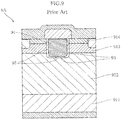
- Fig. 9 shows an example of a conventional vertical insulated-gate semiconductor device having a trench structure.
- the semiconductor device 9A shown in the figure includes a first n-type semiconductor layer 911, a second n-type semiconductor layer 912, a p-type semiconductor layer 913, an n-type semiconductor region 914, a trench 93, a gate electrode 94 and a gate insulating layer 95.
- the first n-type semiconductor layer 911 serves as a base of the semiconductor device 9A.
- the second n-type semiconductor layer 912. the p-type semiconductor layer 913, and the n-type semiconductor region 914 are stacked on the first n-type semiconductor layer 911.
- the trench 93 is formed so as to penetrate through the p-type semiconductor layer 913 and the n-type semiconductor region 914 to reach the second n-type semiconductor layer 912.
- the gate electrode 94 and the gate insulating layer 95 are provided inside the trench 93.
- the gate insulating layer 95 insulates the gate electrode 94 from the second n-type semiconductor layer 912, the p-type semiconductor layer 913 and the n-type semiconductor region 914.
- the gate insulating layer 95 is formed along the inner surface of the trench 93.
- the p-type semiconductor layer 913 includes a channel region.
- the channel region is along the trench 93 and in contact with the second n-type semiconductor layer912 and the n-type semiconductor region 914.
- the on-resistance is low from the viewpoint of reducing energy loss.
- the dielectric withstand voltage is high.
- there is a demand for a reduced threshold voltage so that the semiconductor device can be driven by applying a relatively low voltage to the gate electrode see Japanese Patent Document JP-A-2006-32420 , for example).
- JPH11145457 there is described a vertical field effect transistor with a U-shaped trench which is designed to be reduced in fluctuations for gate-cutoff voltage and protected against a withstand voltage fault due to short channel effects.
- the vertical field effect transistor is equipped with an n + -type silicon substrate, an n-epitaxial layer and a p base region formed by implanting p-type ions into the surface of the n-epitaxial layer.
- An n + source region is formed in the base region and is shallower than it, while a gate electrode is embedded in a trench through the intermediary of a gate oxide film which covers the base and side of the trench.
- the base region is highest in impurity concentration at a point 0.1 ⁇ m or more deeper from its junction interface at the source region.
- a p-type semiconductor region higher in impurity concentration than the p - type semiconductor region is formed under a n + type semiconductor region serving as a source region of the trench gate type power MISFET, causing the p-type semiconductor region to serve as a punch-through stopper layer of the trench gate type power MISFET.
- a channel layer is formed by plural high-acceleration ion implantations where acceleration voltages are different with one another.
- the channel layer is an impurity implanted layer on which diffusion by a heat treatment is not performed.
- the channel layer is allowed to have its impurity concentration substantially uniform in a depth-wise direction of the trenches, by implanting ions of the impurity at plural different times by use of a high-acceleration ion implantation system. Since a second region having almost no influence on a characteristic of the channel layer can be reduced, the channel layer having a minimum necessary depth can be obtained.
- the trenches are thus made shallow, and accordingly a capacitance can be reduced. Furthermore, an on resistance can be made lower by making an epitaxial layer thinner.
- EP-A2-1,132,970 there is described a power semiconductor element which is claimed to be capable of improving short circuit withstand capability while maintaining low on-voltage.
- a p-type base layer of a trench IGBT comprising a p-type collector layer, an n-type base layer formed on the p-type collector layer, the p-type base layer formed on the n-type base layer, and an n-type emitter layer formed on the surface of the p-type base layer
- the point of the highest impurity concentration is located closer to the n-type base layer than the junction with the emitter layer.
- the pinch-off of the channel is generated in the position closer to the n-type base layer than to the junction between the p-type base layer and the n-type emitter layer.
- a semiconductor device comprising a first semiconductor layer having a first conductivity type and made of silicon carbide; a second semiconductor layer made of silicon carbide, provided on the first semiconductor layer and having a second conductivity type opposite to the first conductivity type; a trench penetrating through the second semiconductor layer to reach the first semiconductor layer; an insulating layer formed at a bottom and a side of the trench along an inner surface of the trench; a gate electrode which is insulated by the insulating layer from the first semiconductor layer and the second semiconductor layer and at least part of which is formed inside the trench; and a semiconductor region made of silicon carbide, having the first conductivity type and formed around the trench on the second semiconductor layer.
- the second semiconductor layer includes a channel region that is along the trench and in contact with the first semiconductor layer at a first end and the semiconductor region at a second end opposite to the first end.
- the size of the channel region in a depth direction of the trench is 0.1 to 0.5 ⁇ m.
- An impurity concentration of the second semiconductor layer initially increases starting from the second end, reaches a maximum at a predetermined depth and decreases as proceeding from the semiconductor region toward the first semiconductor layer in the depth direction of the trench.
- a peak impurity concentration along a depth of the channel region is in a range of 4x10 17 cm -3 to 2x10 18 cm -3 .
- the channel region includes a high-concentration region where impurity concentration is equal to or higher than 5 ⁇ 10 17 cm -3 .
- the high-concentration region is in the form of a layer that is in contact with the trench and that spreads in a direction perpendicular to the depth direction.
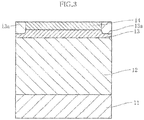
- Fig. 1 depicts a semiconductor device according to a first embodiment of the present invention.
- the semiconductor device A1 includes a first n-type semiconductor layer 11, a second n-type semiconductor layer 12, a p-type semiconductor layer 13, a high-concentration p-type semiconductor region 13a, an n-type semiconductor region 14, a trench 3, a gate electrode 41, a gate insulating layer 5, a source electrode 42, a drain electrode 43 and an interlayer insulating film 6, and has what is known as trench MOSFJET structure.
- the first n-type semiconductor layer 11 is a substrate made of silicon carbide with high-concentration impurity added thereto, and serves as a base of the semiconductor device A1.
- the size of the first n-type semiconductor layer 11 in the depth direction x is approximately 300 ⁇ m.
- the impurity concentration in the first n-type semiconductor layer 11 is approximately 1 ⁇ 10 19 cm -3 .
- the second n-type semiconductor layer 12 is formed on the first n-type semiconductor layer 11.
- the second n-type semiconductor layer 12 is made of silicon carbide with low-concentration impurity added thereto.
- the size of the second n-type semiconductor layer 12 in the depth direction x is approximately 10 ⁇ m.
- the impurity concentration of the second n-type semiconductor layer 12 is approximately 6 ⁇ 10 15 cm -3 .
- the impurity concentration of the second n-type semiconductor layer 12 is not limited to this and may be in a range of approximately 1 ⁇ 10 15 to 2 ⁇ 10 15 cm -3 .
- the p-type semiconductor layer 13 is formed on the second n-type semiconductor layer 12.
- the size of the p-type semiconductor layer 13 in the depth direction x is approximately 0.3 ⁇ m. It is preferable that the size of the p-type semiconductor layer 13 in the depth direction is in a range of 0.1 to 0.5 ⁇ m.
- the impurity concentration of the p-type semiconductor layer 13 is 1 ⁇ 10 17 cm -3 or higher.
- the p-type semiconductor layer 13 includes a channel region.
- the channel region is along the trench 3 and in contact with the second n-type semiconductor layer 12 and the n-type semiconductor region 14.
- the size of the p-type semiconductor layer 13 in the depth direction x needs to be in a range that provides a short channel effect.
- the short channel effect refers to the phenomenon that a decrease in size of the channel region in the depth direction x leads to a lower threshold voltage of the semiconductor device A1.
- the size of the p-type semiconductor layer 13 in the depth direction is smaller than 0.1 ⁇ m, the channel region may often fail to effectively perform its function.
- Fig. 2 shows the distribution of impurity concentration Ic in the depth direction x, in the p-type semiconductor layer 13.
- the impurity concentration Ic With an increase in depth Dp, the impurity concentration Ic becomes higher.
- the impurity concentration Ic is highest at a certain depth Dp, and becomes lower with a further increase in depth Dp.
- the impurity concentration Ic is highest at the depth Dp of approximately 0.5 ⁇ m, and the value at this point is approximately 1 ⁇ 10 18 cm -3 .
- the p-type semiconductor layer 13 includes a high-concentration region 13'. In the figure, the portion where the impurity concentration is 5 ⁇ 10 17 cm -3 or higher is the high-concentration region 13'.
- the size of the p-type semiconductor layer 13 exceeds 0.5 ⁇ m, it is difficult to create such impurity concentration distribution by e.g. impurity ion irradiation and to sufficiently exhibit the short channel effect.
- the n-type semiconductor region 14 is formed on the p-type semiconductor layer 13.
- the size of the n-type semiconductor region 14 in the depth direction x is approximately 0,3 ⁇ m.
- the impurity concentration of the n-type semiconductor region 14 is approximately 1 ⁇ 10 20 cm -3 .
- the impurity concentration of the n-type semiconductor region 14 is not limited to this, and it is only required that the impurity concentration is not lower than 1 ⁇ 10 18 cm -3 .
- the high-concentration p-type semiconductor region 13a is formed on the p-type semiconductor layer 13.
- the trench 3 is formed so as to penetrate through the p-type semiconductor layer 13 and the n-type semiconductor region 14 to reach the second n-type semiconductor layer 12.
- the size of the trench 3 in the depth direction x is equal to or greater than that of the p-type semiconductor layer 13 in the depth direction x. In this embodiment, the size of the trench 3 in the depth direction x is approximately l ⁇ m.
- the gate insulating layer 5 serves to insulate the gate electrode 41 from the second n-type semiconductor layer 12, the p-type semiconductor layer 13, and the n-type semiconductor region 14.
- the gate insulating layer 5 is formed on the inner surface of the trench 3 at the bottom and sides of the trench 3.
- the gate insulating layer 5 is made of, for example, silicon dioxide.
- the size of the side portion of the gate insulating layer 5 in the width direction y is approximately 0.1 ⁇ m.
- the size of the bottom portion of the gate insulating layer 5 in the direction x is approximately 0.08 ⁇ m.
- the source electrode 42 is made of aluminum for example, and in contact with the n-type semiconductor region 14 and the high-concentration p-type semiconductor region 13a.
- the drain electrode 43 is made of aluminum for example, and in contact with the first n-type semiconductor layer 11.
- the drain electrode 43 is formed on the opposite side of the second n-type semiconductor layer 12 across the first n-type semiconductor layer 11.
- the interlayer insulating film 6 is formed so as to cover the gate electrode 41.
- a semiconductor substrate made of silicon carbide, which is to become the first n-type semiconductor layer 11, is prepared.
- the second n-type semiconductor layer 12 is formed on the obverse surface of the substrate by epitaxial crystal growth.
- impurity ions p-type
- impurity ions such as aluminum ions or boron ions are implanted into the upper surface of the second n-type semiconductor layer 12 to thereby form the p-type semiconductor layer 13.
- the impurity ions implanted in the silicon carbide barely diffuse in the silicon carbide substrate.
- the location of the implanted impurity ions in the silicon carbide substrate in the depth direction exclusively depends on the irradiation energy.
- the impurity concentration distribution in the depth direction shown in Fig. 2 is achieved.
- the n-type semiconductor region 14 and the high-concentration p-type semiconductor region 13a are formed, for example by implanting impurity ions (n-type or p-type).
- the trench 3, the gate insulating layer 5 and the gate electrode 41 are formed. Thereafter, the interlayer insulating film 6, the source electrode 42 and the drain electrode 43 are formed. Through the foregoing process, the semiconductor device A1 shown in Fig. 1 is obtained.
- Fig. 5 shows the relationship between peak concentration of impurity in the p-type semiconductor layer (p-type semiconductor layer highest concentration Ch) and threshold voltage Vt in the conventional semiconductor device.
- the short channel effect is not provided and the threshold voltage is not affected by the size of the channel region in the depth direction x, which is the difference from the semiconductor device A1.
- Fig. 6A shows the relationship of threshold voltage Vt and dielectric breakdown field Vb to p-type semiconductor layer highest concentration Ch in the semiconductor device A1 according to this embodiment.
- Fig. 6B shows the relationship of channel resistance Rc and dielectric breakdown field Vb to p-type semiconductor layer highest concentration Ch in the semiconductor device A1 according to this embodiment.
- the threshold voltage Vt is 9 V.
- the channel resistance is 3.8 m ⁇ cm 2 provided that the channel length is 1 ⁇ m and the dielectric breakdown field Vb at a corner portion of the trench 93 is 1.5 MVcm -1 .
- the threshold voltage Vt is 13 V.
- the channel resistance is 5.9 m ⁇ cm 2 under a condition similar to the above, i.e. provided that the channel length is 1 ⁇ m and the dielectric breakdown field Vb at the bottom portion of the trench 93 is 1.5 MVcm -1 .
- the threshold voltage Vt is in a range of 4 V to 11 V when the p-type semiconductor layer highest concentration Ch is in a range of 4 ⁇ 10 17 cm -3 to 2 ⁇ 10 16 cm -3 .
- the dielectric breakdown field Vb is in a range of 0.9 MVcm -1 . to 1.7 MVcm -1 .
- the channel resistance Rc is in a range of 0.5 m ⁇ cm 2 to 2.9 m ⁇ cm 2 .
- the values of threshold voltage Vt, dielectric breakdown field Vb and channel resistance Rc at several points in the above-described range of p-type semiconductor layer highest concentration Ch will be cited.
- the threshold voltage Vt is 4 v.
- the dielectric breakdown field Vb is approximately 0.9 MVcm -1
- the channel resistance Rc is 0.5 m ⁇ cm 2 .
- the threshold voltage Vt is 11 V.
- the dielectric breakdown field Vb is approximately 1.7 MVcm -1
- the channel resistance Rc is 2.9 m ⁇ cm 2
- the threshold voltage Vt is 7 V.
- the dielectric breakdown field Vb is approximately 1.5 MVcm -1
- the channel resistance Rc is 1 m ⁇ cm 2 .
- threshold voltage Vt is maintained at a relatively low level. Presumably, this is because the short channel effect takes place despite that the impurity concentration in the p-type semiconductor layer 13 is set in the foregoing range.
- the dielectric breakdown field Vb is maintained at a relatively high level. This can be construed as a result of the impurity concentration of the p-type semiconductor layer 13 remaining high.
- the channel resistance Rc is relatively small. This can be construed as a result of the reduction in size of the channel region in the depth direction.
- the values of threshold voltage Vt, dielectric breakdown field Vb and channel resistance Rc of the semiconductor device A1 are in a desirable range as a whole. Consequently, the semiconductor device A1 allows the achievement of more desirable values of on-resistance, dielectric withstand voltage and threshold voltage than those of the conventional semiconductor device.
- Figs. 7 and 8 each depict another example of the semiconductor device according to the present invention.
- constituents similar to those of the foregoing embodiment are given the same reference signs, and the description thereof is appropriately omitted.
- Fig. 7 shows a semiconductor device according to a second embodiment of the present invention.
- the semiconductor device A2 according to this embodiment is different from the semiconductor device A1 in having a structure of what is known as an IGBT (Insulated Gate Bipolar Transistor).
- the semiconductor device A2 is similar to the semiconductor device A1 in the size of the channel region and impurity concentration, as well as in including the high-concentration region 13' shown in Fig. 2 and being made of silicon carbide.
- a p-type substrate 15 is provided on the back surface of the n-type semiconductor layer 12.
- a nickel layer 16 is provided between the p-type substrate 15 and the drain electrode 43.
- This structure also allows, as does the semiconductor device A1, the achievement of relatively desirable values of on-resistance, dielectric withstand voltage and threshold voltage. Further, the semiconductor device A2 as an IGBT is advantageous for reducing the resistance, and hence more suitable for use under a high voltage than the semiconductor device A1.
- Fig. 8 shows the semiconductor device according to a third embodiment of the present invention.
- the semiconductor device A3 according to this embodiment is different from the semiconductor device A1 in having a structure of what is known as an SJ (Super Junction) MOSFET.
- the semiconductor device A2 is similar to the semiconductor device A1 in the size of the channel region and impurity concentration, as well as in including the high-concentration region 13' shown in Fig. 2 and being made of silicon carbide.
- a p-type semiconductor layer 17 is formed to sandwich the n-type semiconductor layer 12 in the direction y.
- the p-type semiconductor layer 17 has generally the same thickness as the second n-type semiconductor layer 12, and is in contact with the first n-type semiconductor layer 11 and the p-type semiconductor layer 13. Between the first n-type semiconductor layer 11 and the drain electrode 43, a nickel layer 16 is provided.
- the structure is not limited to this, and the p-type semiconductor layer 17 may be formed along only halfway of the second n-type semiconductor layer 12 from the p-type semiconductor layer 13.
- the first n-type semiconductor layer 11 serves as what is known as a drift layer
- the p-type semiconductor layer 17 as a RESURF layer.
- Such structure also allows, as does the semiconductor device A1, the achievement of relatively desirable values of on-resistance, dielectric withstand voltage and threshold voltage. Further, the semiconductor device A3 as an SJMOSFET is advantageous for achieving both a higher withstand voltage and a lower resistance.
- the semiconductor device according to the present invention is in no way limited to the foregoing embodiments. Specific structure of the constituents of the semiconductor device according to the present invention may be varied in design in various manners.
Landscapes
- Electrodes Of Semiconductors (AREA)
- Insulated Gate Type Field-Effect Transistor (AREA)
Claims (11)
- Halbleiterbauteil (A1, A2, A3) mit:einer ersten Halbleiterschicht (12), die einen ersten Leitfähigkeitstyp (n) hat und aus Siliziumkarbid hergestellt ist;einer zweiten Halbleiterschicht (13), die aus Siliziumkarbid hergestellt ist, die auf der ersten Halbleiterschicht (12) vorgesehen ist und die einen zweiten Leitfähigkeitstyp (p) hat, der entgegengesetzt ist zu dem ersten Leitfähigkeitstyp (n);einem Graben (3), der durch die zweite Halbleiterschicht (13) hindurchgeht, um die erste Halbleiterschicht (12) zu erreichen;einer isolierenden Schicht (5), die an einem Boden und einer Seite des Grabens (3) entlang einer Innenfläche des Grabens (3) gebildet ist;einer Gate-Elektrode (41), die gegenüber der ersten Halbleiterschicht (12) und der zweiten Halbleiterschicht (13) durch die isolierende Schicht (5) isoliert ist, wobei wenigstens ein Teil der Gate-Elektrode (41) innerhalb des Grabens (3) gebildet ist; undeiner Halbleiterregion (14), die aus Siliziumkarbid hergestellt ist, die den ersten Leitfähigkeitstyp (n) hat und die auf der zweiten Halbleiterschicht (13) um den Graben (3) herum gebildet ist;wobei die zweite Halbleiterschicht (13) eine Kanalregion aufweist, die entlang des Grabens (3) vorhanden ist und an einem ersten Ende mit der ersten Halbleiterschicht (12) in Kontakt ist und an einem zweiten Ende, das dem ersten Ende gegenüberliegt, mit der Halbleiterregion (14) in Kontakt ist,wobei eine Größe der Kanalregion in einer Tiefenrichtung des Grabens (3) 0,1 bis 0,5 µm beträgt,wobei eine Spitzen-Verunreinigungskonzentration entlang einer Tiefe der Kanalregion in einem Bereich von 4 x 1017 cm-3 bis 2 x 1018 cm-3 liegt,wobei eine Verunreinigungskonzentration der zweiten Halbleiterschicht (13) ausgehend von dem zweiten Ende anfänglich zunimmt, bei einer vorbestimmten Tiefe ein Maximum erreicht und mit dem Fortschreiten von der Halbleiterregion (14) in Richtung hin zu der ersten Halbleiterschicht (12) in der Tiefenrichtung des Grabens (3) abnimmt.
- Halbleiterbauteil (A1, A2, A3) nach Anspruch 1, wobei die Kanalregion eine Hochkonzentrationsregion (13') aufweist, bei der eine Verunreinigungskonzentration gleich ist oder höher als 5 x 1017 cm-3, und wobei die Hochkonzentrationsregion (13') in der Form einer Schicht vorliegt, die in Kontakt steht mit dem Graben (3) und die sich in einer Richtung senkrecht zu der Tiefenrichtung ausbreitet.
- Halbleiterbauteil (A1, A2, A3) nach Anspruch 1, wobei die isolierende Schicht (5) einen Bodenabschnitt und einen Seitenabschnitt aufweist, die sich in der Dicke voneinander unterscheiden.
- Halbleiterbauteil (A1, A2, A3) nach Anspruch 3, wobei der Seitenabschnitt der isolierenden Schicht (5) dicker ist als der Bodenabschnitt der isolierenden Schicht (5).
- Halbleiterbauteil (A1, A2, A3) nach Anspruch 1, wobei eine Verunreinigungskonzentration der ersten Halbleiterschicht (12) in einem Bereich von 1 x 1015 cm-3 bis 2 x 1016 cm-3 liegt.
- Halbleiterbauteil (A1, A2, A3) nach Anspruch 1, wobei eine Verunreinigungskonzentration der zweiten Halbleiterschicht (13) nicht geringer ist als 1 x 1017 cm-3.
- Halbleiterbauteil (A1, A2, A3) nach Anspruch 1, wobei eine Verunreinigungskonzentration der Halbleiterregion (14) nicht geringer ist als 1 x 1018 cm-3.
- Halbleiterbauteil (A1, A2, A3) nach Anspruch 1, wobei das Halbleiterbauteil als ein Bipolartransistor mit isoliertem Gate konfiguriert ist.
- Halbleiterbauteil (A1, A2, A3) nach Anspruch 1, wobei das Halbleiterbauteil als ein Superjunction-MOSFET konfiguriert ist.
- Halbleiterbauteil (A1, A2, A3) nach Anspruch 1, wobei dann, wenn eine höchste Verunreinigungskonzentration der zweiten Halbleiterschicht (13) in einem Bereich von 4 x 1017 cm-3 bis 2 x 1018 cm-3 liegt, das Halbleiterbauteil (A1, A2, A3) eine Schwellenspannung in einem Bereich von 4 V bis 11 V hat, ein dielektrisches Durchbruchfeld in einem Bereich von 0,9 MVcm-1 bis 1,7 MVcm-1 hat und einen Kanalwiderstand in einem Bereich von 0,5 mΩcm2 bis 2,9 mΩcm2 hat.
- Halbleiterbauteil (A1, A2, A3) nach Anspruch 1, wobei die Spitzen-Verunreinigungskonzentration in einem Bereich von 7 x 1017 cm-3 bis 1,5 x 1018 cm-3 liegt.
Priority Applications (2)
| Application Number | Priority Date | Filing Date | Title |
|---|---|---|---|
| EP19203089.8A EP3614441B1 (de) | 2008-05-20 | 2009-05-20 | Halbleiterbauelement |
| EP22206776.1A EP4156302B1 (de) | 2008-05-20 | 2009-05-20 | Halbleiteranordnung |
Applications Claiming Priority (2)
| Application Number | Priority Date | Filing Date | Title |
|---|---|---|---|
| JP2008131884 | 2008-05-20 | ||
| PCT/JP2009/059257 WO2009142233A1 (ja) | 2008-05-20 | 2009-05-20 | 半導体装置 |
Related Child Applications (3)
| Application Number | Title | Priority Date | Filing Date |
|---|---|---|---|
| EP22206776.1A Division EP4156302B1 (de) | 2008-05-20 | 2009-05-20 | Halbleiteranordnung |
| EP19203089.8A Division EP3614441B1 (de) | 2008-05-20 | 2009-05-20 | Halbleiterbauelement |
| EP19203089.8A Division-Into EP3614441B1 (de) | 2008-05-20 | 2009-05-20 | Halbleiterbauelement |
Publications (3)
| Publication Number | Publication Date |
|---|---|
| EP2293336A1 EP2293336A1 (de) | 2011-03-09 |
| EP2293336A4 EP2293336A4 (de) | 2014-01-29 |
| EP2293336B1 true EP2293336B1 (de) | 2019-11-27 |
Family
ID=41340161
Family Applications (3)
| Application Number | Title | Priority Date | Filing Date |
|---|---|---|---|
| EP22206776.1A Active EP4156302B1 (de) | 2008-05-20 | 2009-05-20 | Halbleiteranordnung |
| EP09750595.2A Active EP2293336B1 (de) | 2008-05-20 | 2009-05-20 | Halbleiterbauelement |
| EP19203089.8A Active EP3614441B1 (de) | 2008-05-20 | 2009-05-20 | Halbleiterbauelement |
Family Applications Before (1)
| Application Number | Title | Priority Date | Filing Date |
|---|---|---|---|
| EP22206776.1A Active EP4156302B1 (de) | 2008-05-20 | 2009-05-20 | Halbleiteranordnung |
Family Applications After (1)
| Application Number | Title | Priority Date | Filing Date |
|---|---|---|---|
| EP19203089.8A Active EP3614441B1 (de) | 2008-05-20 | 2009-05-20 | Halbleiterbauelement |
Country Status (5)
| Country | Link |
|---|---|
| US (2) | US8575622B2 (de) |
| EP (3) | EP4156302B1 (de) |
| JP (2) | JP5819064B2 (de) |
| CN (1) | CN102037564B (de) |
| WO (1) | WO2009142233A1 (de) |
Cited By (1)
| Publication number | Priority date | Publication date | Assignee | Title |
|---|---|---|---|---|
| WO2025068537A1 (en) * | 2023-09-29 | 2025-04-03 | Infineon Technologies Austria Ag | Improved doping for superjunction device |
Families Citing this family (19)
| Publication number | Priority date | Publication date | Assignee | Title |
|---|---|---|---|---|
| JP2012099601A (ja) | 2010-11-01 | 2012-05-24 | Sumitomo Electric Ind Ltd | 半導体装置およびその製造方法 |
| JP2012160584A (ja) * | 2011-02-01 | 2012-08-23 | Sumitomo Electric Ind Ltd | 半導体装置 |
| US8772788B2 (en) | 2011-05-30 | 2014-07-08 | Panasonic Corporation | Semiconductor element and method of manufacturing thereof |
| CN103378141B (zh) * | 2012-04-25 | 2016-03-09 | 上海北车永电电子科技有限公司 | 绝缘栅双极型晶体管及其制作方法 |
| JP6056292B2 (ja) | 2012-09-12 | 2017-01-11 | 住友電気工業株式会社 | 炭化珪素半導体装置の製造方法 |
| JP5811973B2 (ja) | 2012-09-12 | 2015-11-11 | 住友電気工業株式会社 | 炭化珪素半導体装置の製造方法 |
| JP2014056913A (ja) | 2012-09-12 | 2014-03-27 | Sumitomo Electric Ind Ltd | 炭化珪素半導体装置 |
| WO2014102916A1 (ja) * | 2012-12-26 | 2014-07-03 | 株式会社日立製作所 | 炭化珪素半導体装置 |
| JP6048317B2 (ja) * | 2013-06-05 | 2016-12-21 | 株式会社デンソー | 炭化珪素半導体装置 |
| JP2015072999A (ja) * | 2013-10-02 | 2015-04-16 | 株式会社デンソー | 炭化珪素半導体装置 |
| JP6110900B2 (ja) * | 2015-07-07 | 2017-04-05 | ルネサスエレクトロニクス株式会社 | 半導体装置の製造方法 |
| JP6115678B1 (ja) | 2016-02-01 | 2017-04-19 | 富士電機株式会社 | 炭化珪素半導体装置および炭化珪素半導体装置の製造方法 |
| DE102016226237B4 (de) * | 2016-02-01 | 2024-07-18 | Fuji Electric Co., Ltd. | Siliziumcarbid-halbleitervorrichtung |
| EP3227924B1 (de) | 2016-02-02 | 2020-07-22 | ABB Power Grids Switzerland AG | Leistungshalbleiterbauelement |
| JP6784921B2 (ja) * | 2017-02-17 | 2020-11-18 | 株式会社デンソー | スイッチング素子とその製造方法 |
| US10497777B2 (en) | 2017-09-08 | 2019-12-03 | Hestia Power Inc. | Semiconductor power device |
| DE102018200676A1 (de) * | 2018-01-17 | 2019-07-18 | Robert Bosch Gmbh | Leistungselektronisches Bauelement |
| JP2020123607A (ja) * | 2019-01-29 | 2020-08-13 | トヨタ自動車株式会社 | 半導体装置 |
| US12615836B2 (en) | 2022-12-14 | 2026-04-28 | Thinsic Inc. | Trench field effect transistor having improved electrical performance |
Citations (1)
| Publication number | Priority date | Publication date | Assignee | Title |
|---|---|---|---|---|
| EP1132970A2 (de) * | 2000-03-06 | 2001-09-12 | Kabushiki Kaisha Toshiba | Leistungs-Halbleiterelement mit erhöhter Widerstandsfähigkeit gegen Kurzschluss bei niedrigem Durchgangs-Spannungsabfall und Herstellungsverfahren hierfür |
Family Cites Families (14)
| Publication number | Priority date | Publication date | Assignee | Title |
|---|---|---|---|---|
| JPH06101566B2 (ja) * | 1984-04-25 | 1994-12-12 | 株式会社日立製作所 | 縦型電界効果トランジスタ |
| US5742076A (en) * | 1996-06-05 | 1998-04-21 | North Carolina State University | Silicon carbide switching devices having near ideal breakdown voltage capability and ultralow on-state resistance |
| JPH11145457A (ja) * | 1997-11-07 | 1999-05-28 | Nec Corp | 縦型電界効果トランジスタ |
| JP4696335B2 (ja) * | 2000-05-30 | 2011-06-08 | 株式会社デンソー | 半導体装置およびその製造方法 |
| JP2003051598A (ja) * | 2001-05-31 | 2003-02-21 | Hideshi Ito | 高周波パワーmosfet |
| US6919599B2 (en) | 2002-06-28 | 2005-07-19 | International Rectifier Corporation | Short channel trench MOSFET with reduced gate charge |
| JP2004335990A (ja) | 2003-03-10 | 2004-11-25 | Fuji Electric Device Technology Co Ltd | Mis型半導体装置 |
| JP4945055B2 (ja) * | 2003-08-04 | 2012-06-06 | ルネサスエレクトロニクス株式会社 | 半導体装置およびその製造方法 |
| JP3954541B2 (ja) * | 2003-08-05 | 2007-08-08 | 株式会社東芝 | 半導体装置及びその製造方法 |
| JP4404709B2 (ja) | 2004-07-12 | 2010-01-27 | トヨタ自動車株式会社 | 絶縁ゲート型半導体装置およびその製造方法 |
| JP2006080177A (ja) * | 2004-09-08 | 2006-03-23 | Sanyo Electric Co Ltd | 半導体装置およびその製造方法 |
| JP4744958B2 (ja) * | 2005-07-13 | 2011-08-10 | 株式会社東芝 | 半導体素子及びその製造方法 |
| JP4923543B2 (ja) | 2005-11-30 | 2012-04-25 | トヨタ自動車株式会社 | 炭化珪素半導体装置及びその製造方法 |
| JP5101030B2 (ja) | 2006-04-10 | 2012-12-19 | 三菱電機株式会社 | トレンチ型mosfet及びその製造方法 |
-
2009
- 2009-05-20 EP EP22206776.1A patent/EP4156302B1/de active Active
- 2009-05-20 US US12/993,209 patent/US8575622B2/en active Active
- 2009-05-20 CN CN2009801184067A patent/CN102037564B/zh active Active
- 2009-05-20 EP EP09750595.2A patent/EP2293336B1/de active Active
- 2009-05-20 WO PCT/JP2009/059257 patent/WO2009142233A1/ja not_active Ceased
- 2009-05-20 JP JP2010513040A patent/JP5819064B2/ja active Active
- 2009-05-20 EP EP19203089.8A patent/EP3614441B1/de active Active
-
2013
- 2013-10-09 US US14/049,810 patent/US9024329B2/en active Active
-
2014
- 2014-08-07 JP JP2014161371A patent/JP2014241435A/ja active Pending
Patent Citations (1)
| Publication number | Priority date | Publication date | Assignee | Title |
|---|---|---|---|---|
| EP1132970A2 (de) * | 2000-03-06 | 2001-09-12 | Kabushiki Kaisha Toshiba | Leistungs-Halbleiterelement mit erhöhter Widerstandsfähigkeit gegen Kurzschluss bei niedrigem Durchgangs-Spannungsabfall und Herstellungsverfahren hierfür |
Cited By (1)
| Publication number | Priority date | Publication date | Assignee | Title |
|---|---|---|---|---|
| WO2025068537A1 (en) * | 2023-09-29 | 2025-04-03 | Infineon Technologies Austria Ag | Improved doping for superjunction device |
Also Published As
| Publication number | Publication date |
|---|---|
| EP3614441B1 (de) | 2023-04-19 |
| CN102037564B (zh) | 2013-04-10 |
| WO2009142233A1 (ja) | 2009-11-26 |
| JP5819064B2 (ja) | 2015-11-18 |
| US9024329B2 (en) | 2015-05-05 |
| JPWO2009142233A1 (ja) | 2011-09-29 |
| JP2014241435A (ja) | 2014-12-25 |
| US20110068353A1 (en) | 2011-03-24 |
| EP4156302A1 (de) | 2023-03-29 |
| CN102037564A (zh) | 2011-04-27 |
| EP4156302B1 (de) | 2025-11-12 |
| EP2293336A4 (de) | 2014-01-29 |
| EP3614441A1 (de) | 2020-02-26 |
| US8575622B2 (en) | 2013-11-05 |
| EP2293336A1 (de) | 2011-03-09 |
| US20140034969A1 (en) | 2014-02-06 |
Similar Documents
| Publication | Publication Date | Title |
|---|---|---|
| EP2293336B1 (de) | Halbleiterbauelement | |
| US11837629B2 (en) | Power semiconductor devices having gate trenches and buried edge terminations and related methods | |
| EP2966690B1 (de) | Halbleiterbauelement und verfahren zur herstellung davon | |
| US10693002B2 (en) | Semiconductor device | |
| US8252671B2 (en) | Semiconductor device and fabrication method | |
| WO2018106325A1 (en) | Power semiconductor devices having gate trenches with implanted sidewalls and related methods | |
| JP2018537859A (ja) | 半導体装置およびその製造方法 | |
| US20040065920A1 (en) | Short channel trench mosfet with reduced gate charge | |
| US7701001B2 (en) | Short channel trench power MOSFET with low threshold voltage | |
| US10361299B2 (en) | Semiconductor device and method of manufacturing a semiconductor device | |
| WO2023095363A1 (ja) | 半導体装置とその製造方法 | |
| EP2197025B1 (de) | Herstellungsverfahren eines Leistungshalbleiterbauelements | |
| US20090206397A1 (en) | Lateral Trench MOSFET with Conformal Depletion-Assist Layer | |
| US6781203B2 (en) | MOSFET with reduced threshold voltage and on resistance and process for its manufacture | |
| WO2009060406A1 (en) | A trench-gate semiconductor device and method of manufacturing the same |
Legal Events
| Date | Code | Title | Description |
|---|---|---|---|
| PUAI | Public reference made under article 153(3) epc to a published international application that has entered the european phase |
Free format text: ORIGINAL CODE: 0009012 |
|
| 17P | Request for examination filed |
Effective date: 20101203 |
|
| AK | Designated contracting states |
Kind code of ref document: A1 Designated state(s): AT BE BG CH CY CZ DE DK EE ES FI FR GB GR HR HU IE IS IT LI LT LU LV MC MK MT NL NO PL PT RO SE SI SK TR |
|
| AX | Request for extension of the european patent |
Extension state: AL BA RS |
|
| DAX | Request for extension of the european patent (deleted) | ||
| A4 | Supplementary search report drawn up and despatched |
Effective date: 20140108 |
|
| RIC1 | Information provided on ipc code assigned before grant |
Ipc: H01L 21/331 20060101ALN20131220BHEP Ipc: H01L 29/739 20060101ALI20131220BHEP Ipc: H01L 21/336 20060101ALN20131220BHEP Ipc: H01L 29/10 20060101ALI20131220BHEP Ipc: H01L 29/06 20060101ALN20131220BHEP Ipc: H01L 29/16 20060101ALN20131220BHEP Ipc: H01L 29/78 20060101AFI20131220BHEP |
|
| RIN1 | Information on inventor provided before grant (corrected) |
Inventor name: NAKANO YUKI |
|
| STAA | Information on the status of an ep patent application or granted ep patent |
Free format text: STATUS: EXAMINATION IS IN PROGRESS |
|
| 17Q | First examination report despatched |
Effective date: 20180321 |
|
| GRAP | Despatch of communication of intention to grant a patent |
Free format text: ORIGINAL CODE: EPIDOSNIGR1 |
|
| STAA | Information on the status of an ep patent application or granted ep patent |
Free format text: STATUS: GRANT OF PATENT IS INTENDED |
|
| INTG | Intention to grant announced |
Effective date: 20190606 |
|
| GRAS | Grant fee paid |
Free format text: ORIGINAL CODE: EPIDOSNIGR3 |
|
| GRAA | (expected) grant |
Free format text: ORIGINAL CODE: 0009210 |
|
| STAA | Information on the status of an ep patent application or granted ep patent |
Free format text: STATUS: THE PATENT HAS BEEN GRANTED |
|
| AK | Designated contracting states |
Kind code of ref document: B1 Designated state(s): AT BE BG CH CY CZ DE DK EE ES FI FR GB GR HR HU IE IS IT LI LT LU LV MC MK MT NL NO PL PT RO SE SI SK TR |
|
| REG | Reference to a national code |
Ref country code: GB Ref legal event code: FG4D |
|
| REG | Reference to a national code |
Ref country code: CH Ref legal event code: EP |
|
| REG | Reference to a national code |
Ref country code: DE Ref legal event code: R096 Ref document number: 602009060555 Country of ref document: DE |
|
| REG | Reference to a national code |
Ref country code: AT Ref legal event code: REF Ref document number: 1207684 Country of ref document: AT Kind code of ref document: T Effective date: 20191215 |
|
| REG | Reference to a national code |
Ref country code: IE Ref legal event code: FG4D |
|
| REG | Reference to a national code |
Ref country code: NL Ref legal event code: MP Effective date: 20191127 |
|
| REG | Reference to a national code |
Ref country code: LT Ref legal event code: MG4D |
|
| PG25 | Lapsed in a contracting state [announced via postgrant information from national office to epo] |
Ref country code: SE Free format text: LAPSE BECAUSE OF FAILURE TO SUBMIT A TRANSLATION OF THE DESCRIPTION OR TO PAY THE FEE WITHIN THE PRESCRIBED TIME-LIMIT Effective date: 20191127 Ref country code: NL Free format text: LAPSE BECAUSE OF FAILURE TO SUBMIT A TRANSLATION OF THE DESCRIPTION OR TO PAY THE FEE WITHIN THE PRESCRIBED TIME-LIMIT Effective date: 20191127 Ref country code: ES Free format text: LAPSE BECAUSE OF FAILURE TO SUBMIT A TRANSLATION OF THE DESCRIPTION OR TO PAY THE FEE WITHIN THE PRESCRIBED TIME-LIMIT Effective date: 20191127 Ref country code: LT Free format text: LAPSE BECAUSE OF FAILURE TO SUBMIT A TRANSLATION OF THE DESCRIPTION OR TO PAY THE FEE WITHIN THE PRESCRIBED TIME-LIMIT Effective date: 20191127 Ref country code: BG Free format text: LAPSE BECAUSE OF FAILURE TO SUBMIT A TRANSLATION OF THE DESCRIPTION OR TO PAY THE FEE WITHIN THE PRESCRIBED TIME-LIMIT Effective date: 20200227 Ref country code: GR Free format text: LAPSE BECAUSE OF FAILURE TO SUBMIT A TRANSLATION OF THE DESCRIPTION OR TO PAY THE FEE WITHIN THE PRESCRIBED TIME-LIMIT Effective date: 20200228 Ref country code: LV Free format text: LAPSE BECAUSE OF FAILURE TO SUBMIT A TRANSLATION OF THE DESCRIPTION OR TO PAY THE FEE WITHIN THE PRESCRIBED TIME-LIMIT Effective date: 20191127 Ref country code: NO Free format text: LAPSE BECAUSE OF FAILURE TO SUBMIT A TRANSLATION OF THE DESCRIPTION OR TO PAY THE FEE WITHIN THE PRESCRIBED TIME-LIMIT Effective date: 20200227 Ref country code: FI Free format text: LAPSE BECAUSE OF FAILURE TO SUBMIT A TRANSLATION OF THE DESCRIPTION OR TO PAY THE FEE WITHIN THE PRESCRIBED TIME-LIMIT Effective date: 20191127 |
|
| PG25 | Lapsed in a contracting state [announced via postgrant information from national office to epo] |
Ref country code: HR Free format text: LAPSE BECAUSE OF FAILURE TO SUBMIT A TRANSLATION OF THE DESCRIPTION OR TO PAY THE FEE WITHIN THE PRESCRIBED TIME-LIMIT Effective date: 20191127 Ref country code: IS Free format text: LAPSE BECAUSE OF FAILURE TO SUBMIT A TRANSLATION OF THE DESCRIPTION OR TO PAY THE FEE WITHIN THE PRESCRIBED TIME-LIMIT Effective date: 20200327 |
|
| PG25 | Lapsed in a contracting state [announced via postgrant information from national office to epo] |
Ref country code: CZ Free format text: LAPSE BECAUSE OF FAILURE TO SUBMIT A TRANSLATION OF THE DESCRIPTION OR TO PAY THE FEE WITHIN THE PRESCRIBED TIME-LIMIT Effective date: 20191127 Ref country code: RO Free format text: LAPSE BECAUSE OF FAILURE TO SUBMIT A TRANSLATION OF THE DESCRIPTION OR TO PAY THE FEE WITHIN THE PRESCRIBED TIME-LIMIT Effective date: 20191127 Ref country code: DK Free format text: LAPSE BECAUSE OF FAILURE TO SUBMIT A TRANSLATION OF THE DESCRIPTION OR TO PAY THE FEE WITHIN THE PRESCRIBED TIME-LIMIT Effective date: 20191127 Ref country code: PT Free format text: LAPSE BECAUSE OF FAILURE TO SUBMIT A TRANSLATION OF THE DESCRIPTION OR TO PAY THE FEE WITHIN THE PRESCRIBED TIME-LIMIT Effective date: 20200419 Ref country code: EE Free format text: LAPSE BECAUSE OF FAILURE TO SUBMIT A TRANSLATION OF THE DESCRIPTION OR TO PAY THE FEE WITHIN THE PRESCRIBED TIME-LIMIT Effective date: 20191127 |
|
| REG | Reference to a national code |
Ref country code: DE Ref legal event code: R097 Ref document number: 602009060555 Country of ref document: DE |
|
| PG25 | Lapsed in a contracting state [announced via postgrant information from national office to epo] |
Ref country code: SK Free format text: LAPSE BECAUSE OF FAILURE TO SUBMIT A TRANSLATION OF THE DESCRIPTION OR TO PAY THE FEE WITHIN THE PRESCRIBED TIME-LIMIT Effective date: 20191127 |
|
| REG | Reference to a national code |
Ref country code: AT Ref legal event code: MK05 Ref document number: 1207684 Country of ref document: AT Kind code of ref document: T Effective date: 20191127 |
|
| PLBE | No opposition filed within time limit |
Free format text: ORIGINAL CODE: 0009261 |
|
| STAA | Information on the status of an ep patent application or granted ep patent |
Free format text: STATUS: NO OPPOSITION FILED WITHIN TIME LIMIT |
|
| 26N | No opposition filed |
Effective date: 20200828 |
|
| PG25 | Lapsed in a contracting state [announced via postgrant information from national office to epo] |
Ref country code: AT Free format text: LAPSE BECAUSE OF FAILURE TO SUBMIT A TRANSLATION OF THE DESCRIPTION OR TO PAY THE FEE WITHIN THE PRESCRIBED TIME-LIMIT Effective date: 20191127 Ref country code: PL Free format text: LAPSE BECAUSE OF FAILURE TO SUBMIT A TRANSLATION OF THE DESCRIPTION OR TO PAY THE FEE WITHIN THE PRESCRIBED TIME-LIMIT Effective date: 20191127 Ref country code: SI Free format text: LAPSE BECAUSE OF FAILURE TO SUBMIT A TRANSLATION OF THE DESCRIPTION OR TO PAY THE FEE WITHIN THE PRESCRIBED TIME-LIMIT Effective date: 20191127 |
|
| PG25 | Lapsed in a contracting state [announced via postgrant information from national office to epo] |
Ref country code: IT Free format text: LAPSE BECAUSE OF FAILURE TO SUBMIT A TRANSLATION OF THE DESCRIPTION OR TO PAY THE FEE WITHIN THE PRESCRIBED TIME-LIMIT Effective date: 20191127 Ref country code: CH Free format text: LAPSE BECAUSE OF NON-PAYMENT OF DUE FEES Effective date: 20200531 Ref country code: MC Free format text: LAPSE BECAUSE OF FAILURE TO SUBMIT A TRANSLATION OF THE DESCRIPTION OR TO PAY THE FEE WITHIN THE PRESCRIBED TIME-LIMIT Effective date: 20191127 Ref country code: LI Free format text: LAPSE BECAUSE OF NON-PAYMENT OF DUE FEES Effective date: 20200531 |
|
| REG | Reference to a national code |
Ref country code: BE Ref legal event code: MM Effective date: 20200531 |
|
| GBPC | Gb: european patent ceased through non-payment of renewal fee |
Effective date: 20200520 |
|
| PG25 | Lapsed in a contracting state [announced via postgrant information from national office to epo] |
Ref country code: LU Free format text: LAPSE BECAUSE OF NON-PAYMENT OF DUE FEES Effective date: 20200520 |
|
| PG25 | Lapsed in a contracting state [announced via postgrant information from national office to epo] |
Ref country code: IE Free format text: LAPSE BECAUSE OF NON-PAYMENT OF DUE FEES Effective date: 20200520 Ref country code: FR Free format text: LAPSE BECAUSE OF NON-PAYMENT OF DUE FEES Effective date: 20200531 Ref country code: GB Free format text: LAPSE BECAUSE OF NON-PAYMENT OF DUE FEES Effective date: 20200520 |
|
| PG25 | Lapsed in a contracting state [announced via postgrant information from national office to epo] |
Ref country code: BE Free format text: LAPSE BECAUSE OF NON-PAYMENT OF DUE FEES Effective date: 20200531 |
|
| PG25 | Lapsed in a contracting state [announced via postgrant information from national office to epo] |
Ref country code: TR Free format text: LAPSE BECAUSE OF FAILURE TO SUBMIT A TRANSLATION OF THE DESCRIPTION OR TO PAY THE FEE WITHIN THE PRESCRIBED TIME-LIMIT Effective date: 20191127 Ref country code: MT Free format text: LAPSE BECAUSE OF FAILURE TO SUBMIT A TRANSLATION OF THE DESCRIPTION OR TO PAY THE FEE WITHIN THE PRESCRIBED TIME-LIMIT Effective date: 20191127 Ref country code: CY Free format text: LAPSE BECAUSE OF FAILURE TO SUBMIT A TRANSLATION OF THE DESCRIPTION OR TO PAY THE FEE WITHIN THE PRESCRIBED TIME-LIMIT Effective date: 20191127 |
|
| PG25 | Lapsed in a contracting state [announced via postgrant information from national office to epo] |
Ref country code: MK Free format text: LAPSE BECAUSE OF FAILURE TO SUBMIT A TRANSLATION OF THE DESCRIPTION OR TO PAY THE FEE WITHIN THE PRESCRIBED TIME-LIMIT Effective date: 20191127 |
|
| P01 | Opt-out of the competence of the unified patent court (upc) registered |
Effective date: 20230512 |
|
| REG | Reference to a national code |
Ref country code: DE Ref legal event code: R079 Ref document number: 602009060555 Country of ref document: DE Free format text: PREVIOUS MAIN CLASS: H01L0029780000 Ipc: H10D0030600000 |
|
| PGFP | Annual fee paid to national office [announced via postgrant information from national office to epo] |
Ref country code: DE Payment date: 20250402 Year of fee payment: 17 |