EP2293445A2 - Source de courant haute tension et expandeur de tension dans un procédé à basse tension - Google Patents
Source de courant haute tension et expandeur de tension dans un procédé à basse tension Download PDFInfo
- Publication number
- EP2293445A2 EP2293445A2 EP10174233A EP10174233A EP2293445A2 EP 2293445 A2 EP2293445 A2 EP 2293445A2 EP 10174233 A EP10174233 A EP 10174233A EP 10174233 A EP10174233 A EP 10174233A EP 2293445 A2 EP2293445 A2 EP 2293445A2
- Authority
- EP
- European Patent Office
- Prior art keywords
- voltage
- transistors
- current source
- terminal
- expander
- Prior art date
- Legal status (The legal status is an assumption and is not a legal conclusion. Google has not performed a legal analysis and makes no representation as to the accuracy of the status listed.)
- Granted
Links
Images


Classifications
-
- H—ELECTRICITY
- H03—ELECTRONIC CIRCUITRY
- H03K—PULSE TECHNIQUE
- H03K17/00—Electronic switching or gating, i.e. not by contact-making and –breaking
- H03K17/10—Modifications for increasing the maximum permissible switched voltage
- H03K17/102—Modifications for increasing the maximum permissible switched voltage in field-effect transistor switches
Definitions
- the invention relates to semiconductor circuits, and more specifically to a voltage expander and a high voltage current source implemented in a low voltage semiconductor process.
- CMOS complementary metal-oxide-semiconductor
- CMOS complementary metal-oxide-semiconductor
- these modern processes manufacture integrated circuits that operate at low voltages, due to the lowered breakdown voltages of the transistors that are fabricated.
- These low voltage IC's are difficult to interface with circuits operating at higher voltage levels, unless special processes are used that can produce low voltage and high voltage devices in the same IC, but these special processes can have disadvantages such as limited performance capabilities.
- FES functional electrical stimulation
- a high voltage current source and a voltage expander implemented in a low voltage semiconductor process extends the operating voltage range of a stack of transistors to k times the supply voltage Vdd at the output node of the stack without exceeding the breakdown voltage of any of the transistors in the stack.
- the voltage expander uses a diode and a voltage divider to detect the output node voltage changes and generates a plurality of voltages that control the gate voltages for the stack of transistors.
- a high voltage wide swing current source utilizes a transistor to set the output current and the voltage expander to extend the output voltage range of the current setting transistor.
- An additional transistor and another current source ensure that the output current is constant throughout the entire output voltage range between about 0V and k x Vdd.
- Fig. 1 shows a circuit diagram of a high voltage current source 100.
- HV high voltage
- a common way is to connect a number k of transistors 141-0 to 141-(k-1) in series as shown in Fig. 1 .
- Transistor 141-0 sets the output current for current source 140 and transistors 141-1 to 141-(k-1) are a stack of (k-1) transistors.
- the gate voltage Vg0 applied to transistor 141-0 determines the output current of current source 140. In this case, a simple high voltage current sink 100 is realized.
- the gate voltages of the stacked transistors 141-1 to 141-(k-1), Vg1, ..., Vgk-1 are fixed accordingly such that all Vds's are less than 1 x Vdd and approximately equal to (Vout - Vdo)/k, where k is the number of transistors in series and Vdo is the drain voltage of transistor 141-0.
- the voltage at the output Vout can only swing within 1 x Vdd and cannot reach close to ground without exceeding the voltage breakdown limits of individual transistors in the stack. Nevertheless, a simple high voltage source, but with very limited capabilities can be designed using a different polarity of transistors.
- Fig. 2 shows a circuit diagram of voltage expander 250 with wide voltage swing, according to an embodiment of the present invention.
- the voltage expander 250 can extend the voltage swing at the output node 235, which has a typical voltage swing of 1 x Vdd at node 212 to about 0V to k times Vdd at the output 235 of voltage expander 250. Similar to the circuit in Fig. 1 , voltage expander 250 also utilizes a number (k-1) of stacked transistors 210, i.e., 213-1 to 213-k-1.
- the gate voltages Vg1 to Vgk-1 of the stack of transistors 210 depend on the output voltage Vout at node 235 instead of having fixed gate voltage levels or depending on the input voltage, as is known to those skilled in the art.
- the gate voltages Vg1 to Vgk-1 are generated by voltage divider 215 together with a series diode 220 in a diode 220 and voltage divider 215 arrangement that couples between the output 235 of the voltage expander 250 and the bias voltage Vbias at node 217.
- Vbias is set at about 1 x Vdd.
- Diode 225 blocks the flow of current from voltage divider 215 back to the output terminal 235.
- Vgj Vbais for Vout ⁇ Vbais + Vdiode where Vdiode is the diode voltage drop.
- the gate voltages Vgj are linearly proportional to the output voltage for Vout > Vbias + Vdiode and the stacked transistors 210 are operating in the saturation region.
- the stacked transistors 210 were, instead, in the OFF state, no current would be allowed to flow through the stack of transistors 210 for pulling down the output voltage Vout below 1 x Vdd and, hence the output swing will be limited.
- the stack of transistors 210 By operating the stack of transistors 210 in different regions according to the output voltage Vout, it allows the voltage swing at node 212 to be extended from about 1 x Vdd to k x Vdd with all the transistors operating under their voltage breakdown limits.
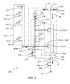
- Fig. 3 shows a circuit diagram of a high voltage wide swing current source according to an embodiment of the present invention.
- Current source 300 includes voltage extender 250, transistors 230 and 225 and current source 240. Using voltage expander 250, a high voltage wide swing current source 300 is shown in Fig. 3 .
- Two transistors 225 and 230 are added to voltage expander 250 and the current source 300 can have a voltage swing from about 0V to k x Vdd. For Vout > Vbias + Vdiode, transistor 230 defines the total current at the output 235 of the voltage expander, Iout.
- Transistor 225 is used for transferring the current flow through the diode 220 and voltage divider 215 arrangement (Ictr) to the drain of transistor 230, Id, such that Id is equal to Ictr + Ist and hence, is equal to Iout.
- the gate voltage of transistor 225, Vgb is set to a value such that Vbias is equal to about 1 x Vdd.
- the gate voltage Vgb of transistor 225 sets the voltage of the second terminal 217 of voltage divider 215. For Vout ⁇ Vbias + Vdiode, transistor 225 will operate in the cut-off region and Vbias may not be well defined.
- the total drain current of transistor 230, Id is equal to Ibias + Ictr + Ist. Since the output current at the voltage expander 250, Iout, is equal to Ictr + Ist, the output current of the high voltage wide swing current source 300 is always constant and equal to Id - Ibias for the entire voltage range between about 0V and k x Vdd when Ibias is added.
- Current source 240 includes transistor 240-0 and a stack of (k-1) transistors 241-1 to 241-k-1 with gate voltages Vs-1 to Vs-k and connected to voltage supply k x Vdd at terminal 245.
- the gate voltage Vs-0 controls the output current for current source 240.
- the voltage expander 250 and the high voltage current source 300 can be made of bipolar junction transistors. In all of these various operational configurations, the voltages across the different terminals of all the transistors are less than the breakdown voltage of any of the transistors.
Landscapes
- Semiconductor Integrated Circuits (AREA)
- Amplifiers (AREA)
- Logic Circuits (AREA)
- Tone Control, Compression And Expansion, Limiting Amplitude (AREA)
Applications Claiming Priority (1)
| Application Number | Priority Date | Filing Date | Title |
|---|---|---|---|
| US23723909P | 2009-08-26 | 2009-08-26 |
Publications (3)
| Publication Number | Publication Date |
|---|---|
| EP2293445A2 true EP2293445A2 (fr) | 2011-03-09 |
| EP2293445A3 EP2293445A3 (fr) | 2012-03-14 |
| EP2293445B1 EP2293445B1 (fr) | 2013-03-06 |
Family
ID=43127138
Family Applications (1)
| Application Number | Title | Priority Date | Filing Date |
|---|---|---|---|
| EP10174233A Active EP2293445B1 (fr) | 2009-08-26 | 2010-08-26 | Source de courant haute tension et expandeur de tension dans un procédé à basse tension |
Country Status (2)
| Country | Link |
|---|---|
| US (1) | US8339189B2 (fr) |
| EP (1) | EP2293445B1 (fr) |
Cited By (2)
| Publication number | Priority date | Publication date | Assignee | Title |
|---|---|---|---|---|
| US8339189B2 (en) | 2009-08-26 | 2012-12-25 | Alfred E. Mann Foundation For Scientific Research | High voltage current source and voltage expander in low voltage process |
| GB2529862A (en) * | 2014-09-04 | 2016-03-09 | Ibm | Current-mode sense amplifier and reference current circuitry |
Families Citing this family (2)
| Publication number | Priority date | Publication date | Assignee | Title |
|---|---|---|---|---|
| US10075157B1 (en) | 2017-04-20 | 2018-09-11 | International Business Machines Corporation | Bidirectional interface using thin oxide devices |
| IL318245B2 (en) * | 2025-01-08 | 2026-01-01 | Applied Materials Israel Ltd | High-voltage power supply and voltage modulator |
Family Cites Families (12)
| Publication number | Priority date | Publication date | Assignee | Title |
|---|---|---|---|---|
| JPS54152845A (en) * | 1978-05-24 | 1979-12-01 | Hitachi Ltd | High dielectric strength mosfet circuit |
| US4193040A (en) * | 1978-11-02 | 1980-03-11 | Western Electric Company, Inc. | High-voltage amplifier with low output impedance |
| FR2587157B1 (fr) * | 1985-09-06 | 1987-11-20 | Thomson Csf | Dispositif de commutation de tension |
| US4900955A (en) * | 1987-05-06 | 1990-02-13 | Sanders Associates, Inc. | Voltage sharing circuit |
| US5382826A (en) * | 1993-12-21 | 1995-01-17 | Xerox Corporation | Stacked high voltage transistor unit |
| US5504444A (en) | 1994-01-24 | 1996-04-02 | Arithmos, Inc. | Driver circuits with extended voltage range |
| JP3926975B2 (ja) | 1999-09-22 | 2007-06-06 | 株式会社東芝 | スタック型mosトランジスタ保護回路 |
| FR2800532B1 (fr) * | 1999-10-28 | 2002-01-04 | Pixtech Sa | Commutateur tres haute tension |
| US6518818B1 (en) | 2001-09-17 | 2003-02-11 | Honeywell International Inc. | High voltage CMOS output driver in low voltage process |
| DE102004039620B4 (de) * | 2004-08-06 | 2006-10-12 | Atmel Germany Gmbh | Integrierte Schaltung, die eine vorgegebene Spannungsfestigkeit besitzt |
| US7649384B2 (en) | 2008-02-05 | 2010-01-19 | Broadcom Corporation | High-voltage tolerant output driver |
| EP2293445B1 (fr) | 2009-08-26 | 2013-03-06 | The Alfred E. Mann Foundation for Scientific Research | Source de courant haute tension et expandeur de tension dans un procédé à basse tension |
-
2010
- 2010-08-26 EP EP10174233A patent/EP2293445B1/fr active Active
- 2010-08-26 US US12/869,442 patent/US8339189B2/en active Active
Non-Patent Citations (1)
| Title |
|---|
| None |
Cited By (2)
| Publication number | Priority date | Publication date | Assignee | Title |
|---|---|---|---|---|
| US8339189B2 (en) | 2009-08-26 | 2012-12-25 | Alfred E. Mann Foundation For Scientific Research | High voltage current source and voltage expander in low voltage process |
| GB2529862A (en) * | 2014-09-04 | 2016-03-09 | Ibm | Current-mode sense amplifier and reference current circuitry |
Also Published As
| Publication number | Publication date |
|---|---|
| EP2293445B1 (fr) | 2013-03-06 |
| US8339189B2 (en) | 2012-12-25 |
| EP2293445A3 (fr) | 2012-03-14 |
| US20110050331A1 (en) | 2011-03-03 |
Similar Documents
| Publication | Publication Date | Title |
|---|---|---|
| CN111210776B (zh) | 栅极驱动电路、显示面板 | |
| CN107005144B (zh) | 用于功率晶体管的调节高压侧栅极驱动器电路 | |
| US10686411B2 (en) | Gate drivers and voltage regulators for gallium nitride devices and integrated circuits | |
| US8575986B2 (en) | Level shift circuit and switching regulator using the same | |
| US7847638B2 (en) | Cascoded circuit | |
| CN108599544B (zh) | 应用于dc-dc变换器的高压使能电路 | |
| CN103529886B (zh) | 调压电路 | |
| US8836380B2 (en) | Bootstrap circuit | |
| CN108631769A (zh) | 宽电压范围输入接口 | |
| EP3550723A1 (fr) | Circuit de suivi de tampon pour tampon de sortie à tolérance d'entrée haute tension | |
| EP2293445B1 (fr) | Source de courant haute tension et expandeur de tension dans un procédé à basse tension | |
| CN101060317B (zh) | 限幅电路和半导体装置 | |
| CN109962704B (zh) | 信号电平转换电路以及显示驱动设备 | |
| US10180694B2 (en) | Adaptive body bias for voltage regulator | |
| US20200350814A1 (en) | Negative voltage generation circuit and power conversion device using same | |
| KR100935843B1 (ko) | I/o 회로 | |
| US20240022175A1 (en) | Power supply device with high efficiency | |
| CN108347243A (zh) | 电平转换器 | |
| KR100691349B1 (ko) | 멀티 파워 시스템에 사용되는 차동 회로, 출력 버퍼 회로및 반도체 집적 회로 | |
| KR20060045372A (ko) | 반도체 장치 | |
| US7508188B2 (en) | On-chip current sensing methods and systems | |
| JP4311683B2 (ja) | 半導体装置、降圧チョッパレギュレータ、電子機器 | |
| EP2824534A2 (fr) | Source de courant modulée en vrac | |
| JPS62229416A (ja) | 電圧制限回路 | |
| US20240329676A1 (en) | Power supply device |
Legal Events
| Date | Code | Title | Description |
|---|---|---|---|
| PUAI | Public reference made under article 153(3) epc to a published international application that has entered the european phase |
Free format text: ORIGINAL CODE: 0009012 |
|
| AK | Designated contracting states |
Kind code of ref document: A2 Designated state(s): AL AT BE BG CH CY CZ DE DK EE ES FI FR GB GR HR HU IE IS IT LI LT LU LV MC MK MT NL NO PL PT RO SE SI SK SM TR |
|
| AX | Request for extension of the european patent |
Extension state: BA ME RS |
|
| RAP1 | Party data changed (applicant data changed or rights of an application transferred) |
Owner name: ALFRED E. MANN FOUNDATION FOR SCIENTIFIC RESEARCH |
|
| RIN1 | Information on inventor provided before grant (corrected) |
Inventor name: LEE, EDWARD K. F. |
|
| PUAL | Search report despatched |
Free format text: ORIGINAL CODE: 0009013 |
|
| AK | Designated contracting states |
Kind code of ref document: A3 Designated state(s): AL AT BE BG CH CY CZ DE DK EE ES FI FR GB GR HR HU IE IS IT LI LT LU LV MC MK MT NL NO PL PT RO SE SI SK SM TR |
|
| AX | Request for extension of the european patent |
Extension state: BA ME RS |
|
| RIC1 | Information provided on ipc code assigned before grant |
Ipc: G05F 3/24 20060101ALI20120208BHEP Ipc: H03K 17/10 20060101AFI20120208BHEP |
|
| 17P | Request for examination filed |
Effective date: 20120830 |
|
| GRAP | Despatch of communication of intention to grant a patent |
Free format text: ORIGINAL CODE: EPIDOSNIGR1 |
|
| RAP1 | Party data changed (applicant data changed or rights of an application transferred) |
Owner name: THE ALFRED E. MANN FOUNDATION FOR SCIENTIFIC RESEA |
|
| GRAS | Grant fee paid |
Free format text: ORIGINAL CODE: EPIDOSNIGR3 |
|
| GRAA | (expected) grant |
Free format text: ORIGINAL CODE: 0009210 |
|
| AK | Designated contracting states |
Kind code of ref document: B1 Designated state(s): AL AT BE BG CH CY CZ DE DK EE ES FI FR GB GR HR HU IE IS IT LI LT LU LV MC MK MT NL NO PL PT RO SE SI SK SM TR |
|
| REG | Reference to a national code |
Ref country code: GB Ref legal event code: FG4D |
|
| REG | Reference to a national code |
Ref country code: AT Ref legal event code: REF Ref document number: 600112 Country of ref document: AT Kind code of ref document: T Effective date: 20130315 Ref country code: CH Ref legal event code: EP |
|
| REG | Reference to a national code |
Ref country code: IE Ref legal event code: FG4D |
|
| REG | Reference to a national code |
Ref country code: DE Ref legal event code: R096 Ref document number: 602010005210 Country of ref document: DE Effective date: 20130502 |
|
| REG | Reference to a national code |
Ref country code: AT Ref legal event code: MK05 Ref document number: 600112 Country of ref document: AT Kind code of ref document: T Effective date: 20130306 |
|
| PG25 | Lapsed in a contracting state [announced via postgrant information from national office to epo] |
Ref country code: AT Free format text: LAPSE BECAUSE OF FAILURE TO SUBMIT A TRANSLATION OF THE DESCRIPTION OR TO PAY THE FEE WITHIN THE PRESCRIBED TIME-LIMIT Effective date: 20130306 Ref country code: LT Free format text: LAPSE BECAUSE OF FAILURE TO SUBMIT A TRANSLATION OF THE DESCRIPTION OR TO PAY THE FEE WITHIN THE PRESCRIBED TIME-LIMIT Effective date: 20130306 Ref country code: ES Free format text: LAPSE BECAUSE OF FAILURE TO SUBMIT A TRANSLATION OF THE DESCRIPTION OR TO PAY THE FEE WITHIN THE PRESCRIBED TIME-LIMIT Effective date: 20130617 Ref country code: BG Free format text: LAPSE BECAUSE OF FAILURE TO SUBMIT A TRANSLATION OF THE DESCRIPTION OR TO PAY THE FEE WITHIN THE PRESCRIBED TIME-LIMIT Effective date: 20130606 Ref country code: SE Free format text: LAPSE BECAUSE OF FAILURE TO SUBMIT A TRANSLATION OF THE DESCRIPTION OR TO PAY THE FEE WITHIN THE PRESCRIBED TIME-LIMIT Effective date: 20130306 Ref country code: NO Free format text: LAPSE BECAUSE OF FAILURE TO SUBMIT A TRANSLATION OF THE DESCRIPTION OR TO PAY THE FEE WITHIN THE PRESCRIBED TIME-LIMIT Effective date: 20130606 |
|
| REG | Reference to a national code |
Ref country code: NL Ref legal event code: VDEP Effective date: 20130306 |
|
| REG | Reference to a national code |
Ref country code: LT Ref legal event code: MG4D |
|
| PG25 | Lapsed in a contracting state [announced via postgrant information from national office to epo] |
Ref country code: GR Free format text: LAPSE BECAUSE OF FAILURE TO SUBMIT A TRANSLATION OF THE DESCRIPTION OR TO PAY THE FEE WITHIN THE PRESCRIBED TIME-LIMIT Effective date: 20130607 Ref country code: LV Free format text: LAPSE BECAUSE OF FAILURE TO SUBMIT A TRANSLATION OF THE DESCRIPTION OR TO PAY THE FEE WITHIN THE PRESCRIBED TIME-LIMIT Effective date: 20130306 Ref country code: SI Free format text: LAPSE BECAUSE OF FAILURE TO SUBMIT A TRANSLATION OF THE DESCRIPTION OR TO PAY THE FEE WITHIN THE PRESCRIBED TIME-LIMIT Effective date: 20130306 Ref country code: FI Free format text: LAPSE BECAUSE OF FAILURE TO SUBMIT A TRANSLATION OF THE DESCRIPTION OR TO PAY THE FEE WITHIN THE PRESCRIBED TIME-LIMIT Effective date: 20130306 |
|
| PG25 | Lapsed in a contracting state [announced via postgrant information from national office to epo] |
Ref country code: BE Free format text: LAPSE BECAUSE OF FAILURE TO SUBMIT A TRANSLATION OF THE DESCRIPTION OR TO PAY THE FEE WITHIN THE PRESCRIBED TIME-LIMIT Effective date: 20130306 Ref country code: HR Free format text: LAPSE BECAUSE OF FAILURE TO SUBMIT A TRANSLATION OF THE DESCRIPTION OR TO PAY THE FEE WITHIN THE PRESCRIBED TIME-LIMIT Effective date: 20130306 |
|
| PG25 | Lapsed in a contracting state [announced via postgrant information from national office to epo] |
Ref country code: CZ Free format text: LAPSE BECAUSE OF FAILURE TO SUBMIT A TRANSLATION OF THE DESCRIPTION OR TO PAY THE FEE WITHIN THE PRESCRIBED TIME-LIMIT Effective date: 20130306 Ref country code: RO Free format text: LAPSE BECAUSE OF FAILURE TO SUBMIT A TRANSLATION OF THE DESCRIPTION OR TO PAY THE FEE WITHIN THE PRESCRIBED TIME-LIMIT Effective date: 20130306 Ref country code: SK Free format text: LAPSE BECAUSE OF FAILURE TO SUBMIT A TRANSLATION OF THE DESCRIPTION OR TO PAY THE FEE WITHIN THE PRESCRIBED TIME-LIMIT Effective date: 20130306 Ref country code: NL Free format text: LAPSE BECAUSE OF FAILURE TO SUBMIT A TRANSLATION OF THE DESCRIPTION OR TO PAY THE FEE WITHIN THE PRESCRIBED TIME-LIMIT Effective date: 20130306 Ref country code: PT Free format text: LAPSE BECAUSE OF FAILURE TO SUBMIT A TRANSLATION OF THE DESCRIPTION OR TO PAY THE FEE WITHIN THE PRESCRIBED TIME-LIMIT Effective date: 20130708 Ref country code: IS Free format text: LAPSE BECAUSE OF FAILURE TO SUBMIT A TRANSLATION OF THE DESCRIPTION OR TO PAY THE FEE WITHIN THE PRESCRIBED TIME-LIMIT Effective date: 20130706 Ref country code: EE Free format text: LAPSE BECAUSE OF FAILURE TO SUBMIT A TRANSLATION OF THE DESCRIPTION OR TO PAY THE FEE WITHIN THE PRESCRIBED TIME-LIMIT Effective date: 20130306 |
|
| PG25 | Lapsed in a contracting state [announced via postgrant information from national office to epo] |
Ref country code: PL Free format text: LAPSE BECAUSE OF FAILURE TO SUBMIT A TRANSLATION OF THE DESCRIPTION OR TO PAY THE FEE WITHIN THE PRESCRIBED TIME-LIMIT Effective date: 20130306 |
|
| PLBE | No opposition filed within time limit |
Free format text: ORIGINAL CODE: 0009261 |
|
| STAA | Information on the status of an ep patent application or granted ep patent |
Free format text: STATUS: NO OPPOSITION FILED WITHIN TIME LIMIT |
|
| PG25 | Lapsed in a contracting state [announced via postgrant information from national office to epo] |
Ref country code: DK Free format text: LAPSE BECAUSE OF FAILURE TO SUBMIT A TRANSLATION OF THE DESCRIPTION OR TO PAY THE FEE WITHIN THE PRESCRIBED TIME-LIMIT Effective date: 20130306 |
|
| 26N | No opposition filed |
Effective date: 20131209 |
|
| PG25 | Lapsed in a contracting state [announced via postgrant information from national office to epo] |
Ref country code: IT Free format text: LAPSE BECAUSE OF FAILURE TO SUBMIT A TRANSLATION OF THE DESCRIPTION OR TO PAY THE FEE WITHIN THE PRESCRIBED TIME-LIMIT Effective date: 20130306 |
|
| REG | Reference to a national code |
Ref country code: DE Ref legal event code: R097 Ref document number: 602010005210 Country of ref document: DE Effective date: 20131209 |
|
| PG25 | Lapsed in a contracting state [announced via postgrant information from national office to epo] |
Ref country code: MC Free format text: LAPSE BECAUSE OF FAILURE TO SUBMIT A TRANSLATION OF THE DESCRIPTION OR TO PAY THE FEE WITHIN THE PRESCRIBED TIME-LIMIT Effective date: 20130306 |
|
| REG | Reference to a national code |
Ref country code: IE Ref legal event code: MM4A |
|
| REG | Reference to a national code |
Ref country code: FR Ref legal event code: ST Effective date: 20140430 |
|
| PG25 | Lapsed in a contracting state [announced via postgrant information from national office to epo] |
Ref country code: IE Free format text: LAPSE BECAUSE OF NON-PAYMENT OF DUE FEES Effective date: 20130826 |
|
| PG25 | Lapsed in a contracting state [announced via postgrant information from national office to epo] |
Ref country code: FR Free format text: LAPSE BECAUSE OF NON-PAYMENT OF DUE FEES Effective date: 20130902 |
|
| REG | Reference to a national code |
Ref country code: CH Ref legal event code: PL |
|
| PG25 | Lapsed in a contracting state [announced via postgrant information from national office to epo] |
Ref country code: CH Free format text: LAPSE BECAUSE OF NON-PAYMENT OF DUE FEES Effective date: 20140831 Ref country code: LI Free format text: LAPSE BECAUSE OF NON-PAYMENT OF DUE FEES Effective date: 20140831 |
|
| PG25 | Lapsed in a contracting state [announced via postgrant information from national office to epo] |
Ref country code: SM Free format text: LAPSE BECAUSE OF FAILURE TO SUBMIT A TRANSLATION OF THE DESCRIPTION OR TO PAY THE FEE WITHIN THE PRESCRIBED TIME-LIMIT Effective date: 20130306 |
|
| PG25 | Lapsed in a contracting state [announced via postgrant information from national office to epo] |
Ref country code: TR Free format text: LAPSE BECAUSE OF FAILURE TO SUBMIT A TRANSLATION OF THE DESCRIPTION OR TO PAY THE FEE WITHIN THE PRESCRIBED TIME-LIMIT Effective date: 20130306 Ref country code: CY Free format text: LAPSE BECAUSE OF FAILURE TO SUBMIT A TRANSLATION OF THE DESCRIPTION OR TO PAY THE FEE WITHIN THE PRESCRIBED TIME-LIMIT Effective date: 20130306 Ref country code: MT Free format text: LAPSE BECAUSE OF FAILURE TO SUBMIT A TRANSLATION OF THE DESCRIPTION OR TO PAY THE FEE WITHIN THE PRESCRIBED TIME-LIMIT Effective date: 20130306 |
|
| PG25 | Lapsed in a contracting state [announced via postgrant information from national office to epo] |
Ref country code: LU Free format text: LAPSE BECAUSE OF NON-PAYMENT OF DUE FEES Effective date: 20130826 Ref country code: MK Free format text: LAPSE BECAUSE OF FAILURE TO SUBMIT A TRANSLATION OF THE DESCRIPTION OR TO PAY THE FEE WITHIN THE PRESCRIBED TIME-LIMIT Effective date: 20130306 Ref country code: HU Free format text: LAPSE BECAUSE OF FAILURE TO SUBMIT A TRANSLATION OF THE DESCRIPTION OR TO PAY THE FEE WITHIN THE PRESCRIBED TIME-LIMIT; INVALID AB INITIO Effective date: 20100826 |
|
| PG25 | Lapsed in a contracting state [announced via postgrant information from national office to epo] |
Ref country code: AL Free format text: LAPSE BECAUSE OF FAILURE TO SUBMIT A TRANSLATION OF THE DESCRIPTION OR TO PAY THE FEE WITHIN THE PRESCRIBED TIME-LIMIT Effective date: 20130306 |
|
| PGFP | Annual fee paid to national office [announced via postgrant information from national office to epo] |
Ref country code: DE Payment date: 20250827 Year of fee payment: 16 |
|
| PGFP | Annual fee paid to national office [announced via postgrant information from national office to epo] |
Ref country code: GB Payment date: 20250827 Year of fee payment: 16 |