EP2294488B1 - Adaptateur rf pour dispositif de terrain à serrage de sécurité intrinsèque à faible tension - Google Patents
Adaptateur rf pour dispositif de terrain à serrage de sécurité intrinsèque à faible tension Download PDFInfo
- Publication number
- EP2294488B1 EP2294488B1 EP09767061.6A EP09767061A EP2294488B1 EP 2294488 B1 EP2294488 B1 EP 2294488B1 EP 09767061 A EP09767061 A EP 09767061A EP 2294488 B1 EP2294488 B1 EP 2294488B1
- Authority
- EP
- European Patent Office
- Prior art keywords
- loop
- adapter
- circuitry
- process control
- hart
- Prior art date
- Legal status (The legal status is an assumption and is not a legal conclusion. Google has not performed a legal analysis and makes no representation as to the accuracy of the status listed.)
- Active
Links
Images







Classifications
-
- H—ELECTRICITY
- H03—ELECTRONIC CIRCUITRY
- H03F—AMPLIFIERS
- H03F3/00—Amplifiers with only discharge tubes or only semiconductor devices as amplifying elements
- H03F3/04—Amplifiers with only discharge tubes or only semiconductor devices as amplifying elements with semiconductor devices only
- H03F3/08—Amplifiers with only discharge tubes or only semiconductor devices as amplifying elements with semiconductor devices only controlled by light
-
- G—PHYSICS
- G01—MEASURING; TESTING
- G01D—MEASURING NOT SPECIALLY ADAPTED FOR A SPECIFIC VARIABLE; ARRANGEMENTS FOR MEASURING TWO OR MORE VARIABLES NOT COVERED IN A SINGLE OTHER SUBCLASS; TARIFF METERING APPARATUS; MEASURING OR TESTING NOT OTHERWISE PROVIDED FOR
- G01D21/00—Measuring or testing not otherwise provided for
-
- G—PHYSICS
- G05—CONTROLLING; REGULATING
- G05B—CONTROL OR REGULATING SYSTEMS IN GENERAL; FUNCTIONAL ELEMENTS OF SUCH SYSTEMS; MONITORING OR TESTING ARRANGEMENTS FOR SUCH SYSTEMS OR ELEMENTS
- G05B19/00—Program-control systems
- G05B19/02—Program-control systems electric
- G05B19/418—Total factory control, i.e. centrally controlling a plurality of machines, e.g. direct or distributed numerical control [DNC], flexible manufacturing systems [FMS], integrated manufacturing systems [IMS] or computer integrated manufacturing [CIM]
- G05B19/4185—Total factory control, i.e. centrally controlling a plurality of machines, e.g. direct or distributed numerical control [DNC], flexible manufacturing systems [FMS], integrated manufacturing systems [IMS] or computer integrated manufacturing [CIM] characterised by the network communication
-
- G—PHYSICS
- G08—SIGNALLING
- G08C—TRANSMISSION SYSTEMS FOR MEASURED VALUES, CONTROL OR SIMILAR SIGNALS
- G08C17/00—Arrangements for transmitting signals characterised by the use of a wireless electrical link
- G08C17/02—Arrangements for transmitting signals characterised by the use of a wireless electrical link using a radio link
-
- H—ELECTRICITY
- H04—ELECTRIC COMMUNICATION TECHNIQUE
- H04N—PICTORIAL COMMUNICATION, e.g. TELEVISION
- H04N23/00—Cameras or camera modules comprising electronic image sensors; Control thereof
- H04N23/80—Camera processing pipelines; Components thereof
- H04N23/81—Camera processing pipelines; Components thereof for suppressing or minimising disturbance in the image signal generation
-
- H—ELECTRICITY
- H04—ELECTRIC COMMUNICATION TECHNIQUE
- H04N—PICTORIAL COMMUNICATION, e.g. TELEVISION
- H04N25/00—Circuitry of solid-state image sensors [SSIS]; Control thereof
- H04N25/40—Extracting pixel data from image sensors by controlling scanning circuits, e.g. by modifying the number of pixels sampled or to be sampled
- H04N25/44—Extracting pixel data from image sensors by controlling scanning circuits, e.g. by modifying the number of pixels sampled or to be sampled by partially reading an SSIS array
- H04N25/445—Extracting pixel data from image sensors by controlling scanning circuits, e.g. by modifying the number of pixels sampled or to be sampled by partially reading an SSIS array by skipping some contiguous pixels within the read portion of the array
-
- H—ELECTRICITY
- H04—ELECTRIC COMMUNICATION TECHNIQUE
- H04N—PICTORIAL COMMUNICATION, e.g. TELEVISION
- H04N25/00—Circuitry of solid-state image sensors [SSIS]; Control thereof
- H04N25/60—Noise processing, e.g. detecting, correcting, reducing or removing noise
- H04N25/617—Noise processing, e.g. detecting, correcting, reducing or removing noise for reducing electromagnetic interference, e.g. clocking noise
-
- G—PHYSICS
- G05—CONTROLLING; REGULATING
- G05B—CONTROL OR REGULATING SYSTEMS IN GENERAL; FUNCTIONAL ELEMENTS OF SUCH SYSTEMS; MONITORING OR TESTING ARRANGEMENTS FOR SUCH SYSTEMS OR ELEMENTS
- G05B2219/00—Program-control systems
- G05B2219/30—Nc systems
- G05B2219/31—From computer integrated manufacturing till monitoring
- G05B2219/31121—Fielddevice, field controller, interface connected to fieldbus
-
- G—PHYSICS
- G05—CONTROLLING; REGULATING
- G05B—CONTROL OR REGULATING SYSTEMS IN GENERAL; FUNCTIONAL ELEMENTS OF SUCH SYSTEMS; MONITORING OR TESTING ARRANGEMENTS FOR SUCH SYSTEMS OR ELEMENTS
- G05B2219/00—Program-control systems
- G05B2219/30—Nc systems
- G05B2219/33—Director till display
- G05B2219/33192—Radio link, wireless
-
- G—PHYSICS
- G05—CONTROLLING; REGULATING
- G05B—CONTROL OR REGULATING SYSTEMS IN GENERAL; FUNCTIONAL ELEMENTS OF SUCH SYSTEMS; MONITORING OR TESTING ARRANGEMENTS FOR SUCH SYSTEMS OR ELEMENTS
- G05B2219/00—Program-control systems
- G05B2219/30—Nc systems
- G05B2219/34—Director, elements to supervisory
- G05B2219/34313—Power supply for communication delivered by, derived from 4-20-mA current loop
-
- H—ELECTRICITY
- H10—SEMICONDUCTOR DEVICES; ELECTRIC SOLID-STATE DEVICES NOT OTHERWISE PROVIDED FOR
- H10F—INORGANIC SEMICONDUCTOR DEVICES SENSITIVE TO INFRARED RADIATION, LIGHT, ELECTROMAGNETIC RADIATION OF SHORTER WAVELENGTH OR CORPUSCULAR RADIATION
- H10F39/00—Integrated devices, or assemblies of multiple devices, comprising at least one element covered by group H10F30/00, e.g. radiation detectors comprising photodiode arrays
- H10F39/10—Integrated devices
- H10F39/12—Image sensors
- H10F39/18—Complementary metal-oxide-semiconductor [CMOS] image sensors; Photodiode array image sensors
-
- Y—GENERAL TAGGING OF NEW TECHNOLOGICAL DEVELOPMENTS; GENERAL TAGGING OF CROSS-SECTIONAL TECHNOLOGIES SPANNING OVER SEVERAL SECTIONS OF THE IPC; TECHNICAL SUBJECTS COVERED BY FORMER USPC CROSS-REFERENCE ART COLLECTIONS [XRACs] AND DIGESTS
- Y02—TECHNOLOGIES OR APPLICATIONS FOR MITIGATION OR ADAPTATION AGAINST CLIMATE CHANGE
- Y02P—CLIMATE CHANGE MITIGATION TECHNOLOGIES IN THE PRODUCTION OR PROCESSING OF GOODS
- Y02P80/00—Climate change mitigation technologies for sector-wide applications
- Y02P80/10—Efficient use of energy, e.g. using compressed air or pressurized fluid as energy carrier
-
- Y—GENERAL TAGGING OF NEW TECHNOLOGICAL DEVELOPMENTS; GENERAL TAGGING OF CROSS-SECTIONAL TECHNOLOGIES SPANNING OVER SEVERAL SECTIONS OF THE IPC; TECHNICAL SUBJECTS COVERED BY FORMER USPC CROSS-REFERENCE ART COLLECTIONS [XRACs] AND DIGESTS
- Y02—TECHNOLOGIES OR APPLICATIONS FOR MITIGATION OR ADAPTATION AGAINST CLIMATE CHANGE
- Y02P—CLIMATE CHANGE MITIGATION TECHNOLOGIES IN THE PRODUCTION OR PROCESSING OF GOODS
- Y02P90/00—Enabling technologies with a potential contribution to greenhouse gas [GHG] emissions mitigation
- Y02P90/02—Total factory control, e.g. smart factories, flexible manufacturing systems [FMS] or integrated manufacturing systems [IMS]
-
- Y—GENERAL TAGGING OF NEW TECHNOLOGICAL DEVELOPMENTS; GENERAL TAGGING OF CROSS-SECTIONAL TECHNOLOGIES SPANNING OVER SEVERAL SECTIONS OF THE IPC; TECHNICAL SUBJECTS COVERED BY FORMER USPC CROSS-REFERENCE ART COLLECTIONS [XRACs] AND DIGESTS
- Y02—TECHNOLOGIES OR APPLICATIONS FOR MITIGATION OR ADAPTATION AGAINST CLIMATE CHANGE
- Y02P—CLIMATE CHANGE MITIGATION TECHNOLOGIES IN THE PRODUCTION OR PROCESSING OF GOODS
- Y02P90/00—Enabling technologies with a potential contribution to greenhouse gas [GHG] emissions mitigation
- Y02P90/80—Management or planning
Definitions
- the present invention relates to industrial process control or monitoring systems. More specifically, the present invention relates to field devices in such systems which are capable of Radio Frequency (RF) communication.
- RF Radio Frequency
- U.S. Patent Publication No. 2005/289276 describes a field device for use in an industrial process control or monitoring system using power supply circuitry that powers radio frequency communication circuitry using power received from a two-wire process control loop.
- EP1202145 A1 discloses field devices comprising a transmitter and/or receiver for wireless data communication, wherein the energy available for wireless data communication in data transmitting or data receiving field devices is evaluated prior to activation of the transmitter and/or receiver of the field device.
- GB2403043 A discloses a method of configuring a wireless enabled field device comprises receiving the field device identification information, which could include a device tag, comparing the identification information to a configuration database, retrieving the configuration information associated with the field device and sending the configuration information to the field device via at least one wireless communication link to configure the field device.
- the identification information could also comprise an updated list of information associated with a plurality of wireless enabled field devices and a message from a controller. Also disclosed is a method of establishing a communication network for use in a process control system.
- control systems are used to monitor and control inventories of industrial and chemical processes, and the like.
- the control system performs these functions using field devices distributed at key locations in the industrial process and coupled to the control circuitry in the control room by a process control loop.
- field device refers to any device that performs a function in a distributed control or process monitoring system, including all devices currently known, or yet to be known, used in the measurement, control and monitoring of industrial processes.
- each field device also includes communication circuitry that is used for communicating with a process control room, or other circuitry, over a process control loop.
- the process control loop is also used to deliver a regulated current and/or voltage to the field device for powering the field device.
- the process control loop also carries data, either in an analog or digital format.
- analog field devices have been connected to the control room by two-wire process control current loops, with each device connected to the control room by a single two-wire control loop.
- a voltage differential is maintained between the two wires within a range of voltages from 12-45 volts for analog mode and 9-50 volts for digital mode.
- Some analog field devices transmit a signal to the control room by modulating the current running through the current loop to a current proportional to the sensed process variable.
- Other analog field devices can perform an action under the control of the control room by controlling the magnitude of the current through the loop.
- the process control loop can carry digital signals used for communication with field devices.
- wireless technologies have begun to be used to communicate with field devices.
- completely wireless installations are used in which the field device uses a battery, solar cell, or other technique to obtain power without any sort of wired connection.
- the majority of field devices are hardwired to a process control room and do not use wireless communication techniques.
- "intrinsic safety" standards must be implemented which limit the amount of stored energy which can be discharged into the environment.
- the present invention provides an adapter for coupling to a process control transmitter of the type used to monitor a process variable in an industrial process, as defined in appended claim 1.
- Figure 1 is a simplified block diagram of a process control or monitoring system 10 in which a control room or control system 12 couples to a field device 14 over a two-wire process control loop 16.
- the field device 14 includes I/O power circuitry 18, actuator/transducer 20 and wireless communication circuitry 22.
- the wireless communication circuitry 22 is configured to send and/or receive an RF signal 24 using an antenna 26.
- a local display requires direct visual access to the field device. Further, typically an operator can only view a single meter at a time. The instruments which contain the meter are often not at a convenient location or viewing angle.
- One technique which has been used to address such a configuration is the use of a meter which is wired to a process transmitter. This allows the meter to be mounted at a more convenient location. Another technique is shown and described in U.S. patent application Serial No. 10/128,769, filed April 22, 2002 , entitled PROCESS TRANSMITTER WITH WIRELESS COMMUNICATION LINK.
- an RF communication module is configured as an adapter to retrofit a field device which can be used in addition to the connection to a process control loop such as loop 16.
- the wireless communication module 22 can be configured to be compact and lower power such that it can be easily included in existing field device configurations.
- the module can be used for wireless transmission of information for use in monitoring control and/or display of data.
- Such a radio transmitter can make the field device information available in a local area.
- a single local display such as display 32 can be provided and used to display information from the field device 14.
- the display 32 can be configured to display information from several devices, either simultaneously, sequentially, or through commands provided to the display, for example using a manual input such as buttons available to an operator.
- the display 32 can be placed at a fixed location or can be a portable device such that it can be carried throughout the process control system to monitor and observe operation of various field devices. Depending on the strength of the RF signal 24 and the sensitivity of the transmit and receive circuitry, the area covered by the RF transmission can be controlled as desired.
- Figure 2 is a simplified diagram of a process control system 50 in which a number of field devices 14 are coupled to the control room 12 through individual process control loops 16. Each field device 14 transmits an RF signal 24 for receipt by display 32.
- display 32 is capable of displaying four process variables (PV1, PV2, PV3 and PV4) which are received from the field devices 14 using antenna 52.
- the display 32 can be a fixed display or can be a portable display, such as a hand held unit.
- the display 32 is illustrated as showing two process variables which relate to process pressure and two process variables which relate to process temperature.
- This allows the field devices 14 to provide information over the RF connection within a desired range, for example, within a local area. For example, if the display 32 is within 40 meters of a field device 14, it will be capable of receiving and displaying information from that field device.
- An optional user input 48 can be used to, for example, select the format of the display, the process variable displayed, or used to interrogate a field device 14.
- the wireless communication circuitry 22 can be selected as desired.
- One example circuit is the "I-Bean" transmitter device available from Millennial Net. However, other circuitry can be used. Analog or digital signals carried on process control loop 16 can be read and transmitted using the wireless communication circuit 22 without disrupting operation of the process control loop 16 or field device circuitry 68.
- the circuitry used for wireless transmission should be sufficiently small and low powered to fit within the physical and power constraints of process field devices.
- Some prior art transmitters are configured to receive an optional display arranged generally in the position shown for wireless communication circuit 22 in Figure 3 . In such a configuration, the wireless communication circuit 22 can be used in place of the local display. In such a configuration, the communication wireless circuitry 22 simply transmits an RF signal which couples directly to the process control loop 16 and transmits an RF signal which corresponds to any analog and/or digital signals carried on the loop 16.
- the process control loop discussed herein can comprise any type of process control loop for use in industrial process control and monitoring systems.
- Such loops include 4-20mA current loops in which a analog current level is varied between 4 and 20mA to transmit information.
- the same control loop can be used to provide power to the field device.
- Another type of process control loop is in accordance with the HART@ communication protocol in which digital transmissions are superimposed on the 4-20mA signal for transmission of additional information.
- Another example two-wire process control loop uses a protocol set forth by the Instrument Society of America (ISA) which is called the Field Bus SP50 protocol. However, end signaling protocol can be used.
- Some process control loops are configured to connect to multiple field devices such that the field devices can communicate with one another or monitor transmissions from another field device.
- any type of information transmitted on such process control loops, or available or generated internally or received by a field device, or otherwise used to control a field device or other type of information can be transmitted using the wireless communication techniques of the present invention.
- a hand held unit or device used to configure field devices can be carried into the field by an operator. The operator uses the hand held device to send or receive information to a field device when the hand held device is within proximity of the field device. This allows the operator to gather information or program a field device without having to physically couple to the device or the physical process control loop.
- the wireless communication circuitry can transmit continuously or on a periodic or intermittent basis, as desired. In another example, the wireless communication circuitry only transmits when activated or "polled". The activation can be from a source internal to the field device, received through the process control loop, received from a wireless source, or received or generated by another source. In environments in which multiple field devices may transmit simultaneously, the transmission protocol should be selected to avoid or address any type of collisions which might interfere with the transmissions.
- the transmission includes error detection or correction information, this information can be used to detect an error in the transmission and/or correct any errors in the transmissions. If an error is not correctable, the receiving unit can request a re-transmission of the corrupt data or, can indicate an error, or can wait for a subsequent transmission of the data, or take other steps as desired.
- Figure 3 also shows an example hand held device 80 for communication with circuitry 22 over RF connection 82.
- Hand held device 80 includes a display 84 and user input 86. Other types of inputs and outputs can be included in hand held device 80.
- the hand held device 80 is battery operated and can be carried into the field by an operator for communication with field device 60. Information from the field device 60, or from other sources, is displayed on display 84 and the hand held device is controlled using input 86. Commands or other information can be transmitted by the hand held device 80 to field device 60.
- the wireless communication circuitry requires power which is within the power constraints available in the field device. For example, one display currently used within field devices uses 3.6 volts at 0.5 mA. If a transmitter which is capable of operating an LCD meter is employed, the wireless communication circuitry can replace the LCD meter and use the same power source that is used to drive the LCD meter. In another example, the wireless communication circuitry is powered directly from the process control loop, for example using the voltage developed across a diode drop connected in series with the process control loop. In embodiments in which no battery is used with the communication circuitry, the circuitry can more easily meet intrinsic safety or other safety approval requirements and provide an indefinite field life without battery replacement or maintenance. In configurations in which the wireless configuration is only for sending information, power requirements can be reduced.
- a stationary device such as display 32 as illustrated in Figure 1 can include an RF repeater for re-transmission of data received from, or sent to, a field device.
- the RF repeater can be loop powered, or can derive its power from other sources. Further, once the RF data is received, it can be reformatted for transmission over other medium, for example an Ethernet connection, into existing data transmission structures used within process control systems, over an extended range RF communication link such as a cell phone, or relaying using another technique.
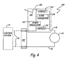
- FIG. 4 is a simplified diagram of a process controller or monitoring system 100 which illustrates another aspect of the present invention.
- a field device 14 connects to a control system 12 through process control loop 16 through junction box 102.
- a field device 104 couples to the process control loop 16 and includes wireless communication circuitry 122.
- the wireless communication circuitry 122 is configured to send an RF signal 106 and to be completely powered by power received from the process control loop 16.
- Process device 104 includes a power regulator 110, a shunt or bypass 112, and a super capacitor 114.
- the super capacitor 114 is slowly charged (trickle charged) using a power regulator 110 by using excess voltage tapped from the process control loop 16.
- the bypass 112 allows loop 16 to operate normally and is connected in series with loop 16.
- Communication circuit 122 includes circuitry for receiving analog and/or digital information carried on process control loop 16. The circuit 122 can responsively transmit an RF signal 106 based upon the received information. If operated as a receiver, circuitry 122 is capable of modulating data onto the electrical current carried in the loop 16. This can be either analog or digital information. This configuration allows data to be relayed over a wireless communication network.
- FIG. 5 is a simplified schematic diagram of field device 104 showing super capacitor 114 in greater detail.
- super capacitor 114 comprises two 10 Farad capacitors configured to each carry a 2.5 volt potential. This yields an equivalent capacitance of 5 farads with a 5 volt potential drop.
- Figure 6 is a graph of voltage versus time measured across super capacitor 114.
- a typical power supply used to provide power to a process control loop provides 24 volts DC.
- a transmitter may only require 12 volts to operate. Wiring losses in the process control loop may cause 2 to 4 volts of voltage drop.
- the burst time is reduced to one millisecond and the resulting transmit time is 0.03 seconds.
- diagnostic data can easily be transmitted because it is not of a time critical nature.
- control and process variable signals can also be transmitted wirelessly.
- any energy storage device can be employed including a battery, or other.
- the energy that is used to charge the storage device can be electrical or magnetic and can be derived or collected from any source.
- FIG 7 is a simplified diagram of process controller monitoring system 150 which includes a control room 152 coupled to a field device 154 through two-wire process control loop 156.
- Process control loop 156 extends across an intrinsic safety barrier 158.
- the control room 152 is modeled as including a power supply 160 and a load resistance 162.
- the field device 154 can be of any configuration and is not limited to the specific schematic shown in Figure 7 .
- RF communication circuitry 170 is shown coupled in series with loop 156.
- Circuitry 170 can be implemented in a terminal block of a field device.
- circuitry 170 can be configured as an add on module such that the two-wire process control loop 156 can connect to existing transmitter circuitry.
- the communication circuitry 170 enables wireless communication abilities to be added to a new or existing process control loop or field device.
- the circuitry is configured to be powered by the process control loop and can be installed anywhere in the loop ranging from the control room, anywhere along the loop itself, in the intrinsic safety (IS) barrier or junction box 158, as a stand alone field device, or included in another field device.
- the circuitry can be configured for any type of communication.
- the circuit 170 is configured to measure the current carried in process control loop 156 and transmit an output related to the measured current to a wireless receiver.
- a sense resistance 180 and a power supply diode 182 couple in series with process control loop 156.
- the sense resistance 180 can be, for example, 10 ohms and is used in sensing the current level I carried in the process control loop 156.
- a test diode 184 is also coupled in series with the loop 156 and provides a test point 186. This can be used to calibrate or characterize a field device coupled to circuitry 170.
- An intrinsic safety protection circuit 190 is provided which includes diode 192 connected as shown across diode 182 and isolation resistors 194 connected at opposed ends of sense resistance 180.
- Diode 182 is part of a power supply 196 which includes capacitor 198, input filter 200, regulator 202, capacitor 204 and secondary filter 206.
- Secondary filter 206 includes capacitor 208 and resistor 210.
- the power supply circuitry 196 generates a power supply voltage V DD relative to a circuit ground for use by circuitry in measuring the loop current and wirelessly transmitting a resultant signal. Although a specific power supply implementation is shown, any appropriate power supply configuration or embodiment may be used as desired.
- the circuitry 170 illustrated in Figure 7 can be implemented on a single printed circuit board such that RF antenna 240 is formed integral with the board. This configuration allows the circuitry 170 to be easily implemented in existing field devices and does not require the use of an external antenna. This reduces installation complexity.
- the wireless communication circuitry does not require an operator to remove covers on equipment such as transmitters or junction boxes in order to expose loop wiring for physical connection to the process control loop. This can be particularly beneficial in hazardous locations where explosive gases or vapors may be present.
- a digital or analog process variable can be sensed by the wireless communication circuitry and transmitted to a wireless meter or hand held device as discussed above.
- Zener diode 182 acts as a shunt element which is placed in series with the loop 156 to develop a preregulated voltage on the input filter stage. Any portion of the loop current which is not used by circuitry 170 is shunted through zener diode 182.
- the input filter 200 can comprise capacitive, inductive and resistive elements and is used to isolate the loop from any noise or load fluctuation generated by circuitry 170. This also suppresses noise in the HART ® extended frequency band in order to conform with HART ® standards.
- the microprocessor 224 including A/D converter, along with the RF circuitry 232 and input circuitry 218 can be placed into a sleep mode or low power mode during periods of idle operation in order to reduce power drain. For example, at a selected interval such as every 10 seconds, an internal timer in the microprocessor can enable the measurement of the loop current by the A/D converter. The measurement circuitry is allowed to settle before the A/D conversion occurs. After the A/D conversion is completed, both the loop measurement circuitry and the A/D converter are turned off to conserve power. The microprocessor passes the measured value to the RF circuitry 232 for transmission. Upon completion of the transmission, the microprocessor and RF circuitry return to the low power mode until the next cycle. The microprocessor may even put itself to sleep temporarily to save power. Using these power management techniques, the microprocessor is able to manage overall current requirements of the circuit by staggering the load demands on the regulator stage.
- HART ® circuitry 230 allows the circuitry 170 to selectively listen to a HART ® message on the 4-20mA signal carried on the current loop 156. Information such as measured process variables, diagnostic information, or other information can be transmitted to a wireless receiver. Further, if the HART ® circuitry 230 is configured to modulate a digital signal onto the process control loop, it can be used to remotely command or interrogate a field device coupled to the loop 156. For example, the HART ® circuitry 230 can be configured to act as a secondary master on the 4-20mA current loop. This, in conjunction with RF circuitry 232 configured as a full transceiver, enables bi- directional communication and configuration of field device from a wireless master unit, for example a hand held device 80 shown in Figure 3 .
- Circuitry 170 is preferably configured to allow operation in hazardous locations and to meet the appropriate approval and specifications, such as intrinsic safety standards.
- the intrinsic safety protection 190 along with intrinsically safety rated resistor 180 is used on the input to the circuitry 170.
- the addition of a redundant zener diode 192 in parallel with zener 182 provides a level of redundancy and limits the amount of voltage that can enter this circuit in an intrinsic safety protected system.
- the sense resistor 180 can be used to limit the maximum current that can enter the circuit 170 and snub any discharge of stored energy from the circuit through its external terminals. This provides an equivalent capacitance of substantially zero.
- the loop measurement circuitry is further protected by two intrinsic safety rated high value resistors 194 connected between the two ends of the sense resistor 180 and the filter 220.
- Other circuit components can be protected from any outside energy sources by the use of potting material or the like which also prevents hazardous gases and vapors from reaching any internal storage elements and nodes in the circuitry 170. For other non-hazardous locations, intrinsic safety components may not be required.
- any host whether it be a process control system, or a portable handheld communicator, must physically connect to wires that are connected to the process transmitter in order to communicate with it.
- the host may wirelessly "connect" to a desired process transmitter from any location in the process plant within communication range.
- the user in a wired system, the user must remove the cover from the device in order to gain access to the terminals for connecting a handheld communicator to perform diagnostics or commissioning of the process transmitter. Removing the cover may require the user to take several safety precautions to ensure that the safety features of the process transmitter, or the facility, are not compromised. Further, removing the cover from a process transmitter may require special work procedures, or even process or partial plant shutdowns, if the transmitter is used in a potentially hazardous area in the process plant. A process transmitter with wireless communications capability does not require the removal of the cover, and the related procedures, in order to communicate either locally or from a distant location.
- the device interfaces the existing HART ® enabled process transmitter to a wireless network.
- This device can act as a communications translator, communicating via HART ® to the existing process transmitters, and communicating over a wireless network to a wireless host or other remote monitoring or diagnostic system.
- another power source for this communications module is not required. The module should operate from the same power that is already provided to the process transmitter, while not negatively impacting the power available for the process transmitter.
- This communication device may operate from solar power, but that is not practical in many installations. It may also operate off a battery. However, batteries have special safety drawbacks when used in process plants adding to their expense, and also require periodic replacement, making them undesirable.
- a mesh network is one in which each wireless device may serve as a router for the other wireless devices. This ensures that each device in the network has the most reliable communications path back to the host. These communication paths are established when the network is initially established, as well as whenever a new device joins the network.
- a process control transmitter which is coupled to a two-wire process control loop be also able to communicate information on a wireless network. It may also be desirable that the device function as a router in a "mesh network.” Further, in many instances it is preferable that the device operate using power from the process control loop rather than requiring a separate source of power.
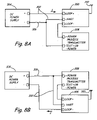
- FIG 8A and 8B show two example wiring configurations for a wireless adapter 300 in accordance with one example embodiment.
- Wireless adapter 300 is shown coupled to a process control loop 302 which is powered by a DC power supply 304.
- the loop is illustrated as including a load resistance 306 and also couples to a process variable transmitter 308.
- the wireless adapter 300 includes two loop connections (Loop+ and Loop-) which connect in series with the process control loop 302. One of the loop connections couples to the power supply 304 while the other loop connection couples to a loop connection of the process transmitter 308.
- the wireless adapter 300 includes a third connection (labeled HART@) which couples to the other loop connection of the process transmitter 308.
- the Loop- connection of adapter 300 couples to the plus connection of transmitter 308 while the HART ® connection of adapter 300 couples to the minus connection (labeled "Test+ or - Power") connection of transmitter 308.
- the arrangement in Figure 8B is slightly different in which the Loop+ connection of the adapter 300 couples to the minus connection of transmitter 308 while the Loop- connection of adapter 300 couples to the power supply 304 and the HART ® connection couples to the plus connection of transmitter 308.
- the adapter 300 is also illustrated with an antenna 310.
- the adapter 300 is configured as a three terminal device through which all of the loop current I flows.
- the separate HART ® connection is used to provide digital communication on the two wire process control loop 302.
- the adapter is not limited to operating in accordance with the HART@ communication protocol and may use any appropriate protocol including Fieldbus protocols.
- the adapter 300 is powered using power received from the process control loop 302.
- the loop 302 is also used to provide power to the transmitter 308.
- the adapter 300 regulates its voltage to a small value, for example 1.0 volts, such that it will have a minimal impact on the process control loop 302.
- the adapter 300 operates using the current available from the loop 302. For example, if the transmitter 308 sets the loop current to a value of 5 mA, the adapter 300 will operate on this 5 mA. If the voltage drop across the adapter is 1 volt, a total of 5 mW will be used by the adapter 300.
- the loop current is varied between 4 mA and 20 mA based upon a measured process variable.
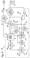
- adapter 300 includes a microcontroller 340 which also includes a memory and a modem for communication.
- the memory is used to store programming instructions, configuration data, variables, etc.
- HART ® analog circuitry 342 is configured to couple to the process variable transmitter 308 through a DC blocking capacitor 346.
- a radio module 344 is provided to enable adapter 300 to communicate using RF communication techniques.
- a regulator 348 is provided which is configured as a DC to DC converter.
- a current shunt circuit 350 is connected in parallel with regulator 348 and includes a bypass transistor 352 controlled by a OP amp 354.
- OP amp 354 operates based upon a difference between a reference voltage (V ref ) and the voltage applied to the regulator 348.
- Regulator 348 provides a 2.3 volt output to a low dropout (LDO) regulator 360.
- Low dropout (LDO) regulator 360 provides a regulated 2 volt power supply output to the microprocessor 340, HART analog circuits 342, reset circuit 382 and ADC 380.
- the adapter 300 is preferably configured to use power from the loop 302 in a very efficient manner. In one specific configuration, this can be achieved by using a low power microcontroller 340, for example, Texas Instruments MSP430F1481 and by using low power analog circuit components. These components can be powered by a low supply voltage to also minimize the total circuit power consumption. Further, the microcontroller 340 can be configured to enter a "sleep" mode if desired when certain functions are not needed, for example communication functions. In the configuration shown in Figure 9 , a separate modem is not utilized. Instead, the microcontroller 340 is used to provide modem functionality.
- the radio module 344 It is also preferable to provide the radio module 344 with a large amount of power. This allows more frequent communication and increased reliability.
- the additional power can be used to publish information from the transmitter 308, allow the adapter 300 to be used as a router for other process transmitters, for example in a mesh network and allow higher transmit power to be used. This can result in a more reliable mesh network, as the path from another wireless device through the adapter 300 to a host may be more reliable than the path which is directly from the device to the host.
- the radio module 344 is powered by super capacitor 320. Therefore, in order to increase the power which is provided to the radio module 344, it is preferable to increase the power stored by super capacitor 320. In the configuration of Figure 9 , this is achieved by arranging the super capacitor 320 as a shunt element for the regulator 348 which regulates the voltage drop across the terminals which couple to loop 302 in conjunction with OP amp 354 and shunt transistor 352. In Figure 9 , the voltage across the loop terminals which couple to the process control loop 302 is regulated to one volt. This is achieved by adjusting the current going to the super capacitor using OP amp 354 and shunt transistor 352.
- regulator 348 operates in series with the loop 302 and is in the feedback loop formed by OP amp 354.
- a separate one volt shunt regulator and super capacitor charging circuit may be implemented. However, this requires additional components and additional power to operate.
- any loop current which is not used by the circuitry of adapter 300 is directed into shunt capacitor 320 for increased efficiency. This results in the maximum amount of power being available for radio module 344.
- the voltage clamp 370 determines the voltage to which capacitor 320 is charged. Once the super capacitor 320 reaches the voltage set by the voltage clamp 370, the excess current flows through clamp 370 rather than into capacitor 320.
- DC to DC converter 348 is configured as a low power "step up" switching regulator that operates with an input voltage of 1 volt. Regulator 348 increases the 1 volt input voltage to a sufficiently high voltage to power the remaining circuitry. In the example of Figure 9 , this is 2.3 volts.
- the converter can be a switched capacitor type converter, an inductor based boost converter, a transformer based converter or other appropriate configuration.
- the LDO regulator 360 regulates the 2.3 volt output from regulator 348 to 2.0 volts and removes any switching noise from the regulator 348.
- the output from the LDO regulator 360 is used to power the microprocessor 340, HART ® analog circuits 342, memory, reset circuitry 382, and analog to digital converter 380.
- HART ® analog circuit block 342 can comprise, for example, a carrier detect circuit, a receive circuit and a transmit circuit. Preferably, these circuits are configured to have low power requirements while maintaining acceptable communications integrity.
- the memory in microprocessor 340 can be used to store programming code and temporary variables. Timers which are internal to microprocessor 340 can be used to provide a "software" modem functionality.
- the memory of the microprocessor 340 may include internal flash memory, RAM as well as EEPROM or other non volatile memory.
- the microcontroller 340 can be configured to monitor the voltage access super capacitor 320 using analog to digital converter 380 which provides a digital output to microcontroller 340 representative of the capacitive voltage.
- the microcontroller 340 can be configured to adjust the voltage drop across the loop terminals which couple to loop 302.
- an optional control line 341 from the microcontroller 340 can be coupled to the inverting input of OP amp 354 of the shunt circuitry 350.
- additional power may be made available to the radio by increasing the loop voltage drop under appropriate conditions.
- the voltage drop can be decreased. However, this will provide less power to the radio module and other circuitry of adapter 300 and may degrade performance.
- FIG 10 is a cross-sectional view of one embodiment showing a process control transmitter 400 coupled to a wireless adapter 300.
- Transmitter 400 includes a sensor 64 and measurement circuitry 66 as discussed above. Measurement circuitry 66 couples to field device circuitry 68.
- Transmitter 400 couples to two wire process control loop 302 through a connection block 406 and the wireless adapter 300. Further, the wireless adapter 300 couples to the housing of transmitter 400. In the example shown in Figure 10 , the coupling is through a NPT conduit connection 409. A similar conduit connection 409 is also used to couple to conduit 411 for carrying the two wire process control loop 302 therethrough.
- the chassis of wireless adapter 300 couples to an electrical ground connection 410 of transmitter 400 through wire 408.
- the wireless adapter may require more power.
- the device may require 60 mW of power (3 volts at 20 mA) in order to transmit a wireless message.
- the power required to receive a wireless transmission may also exceed the instantaneous power which is available from the process control loop.
- the wireless adapter be able to store power internally for use when there is insufficient power instantaneously available from the two wire process control loop.
- circuitry is provided to limit the amount of power which the wireless adapter 300 is capable of discharging back into the process control loop 302 or elsewhere.
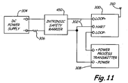
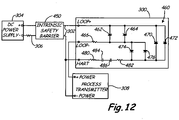
- FIG 12 is a simplified block diagram showing wireless adapter 300 including one example configuration of intrinsic safety circuitry 460.
- zener diodes 462 and 464 are provided which can comprise, for example, zener diode having a 6.2 volt bias voltage coupled across the loop+ and loop- connections.
- a 5 ohm resistance 466 is coupled in series with the two wire process control loop 302.
- Diodes 470 and 472 are coupled across the loop+ connection and the HART ® connection to the field device 308.
- diodes 474 and 476 are coupled across the loop- connection and the HART ® connection to the field device 308.
- Resistors 480 and 482, and capacitors 484 and 486 are connected in series with the HART@ connection to the field device 308.
- resistor 480 has a value of 49.9 ohms
- resistance 482 has a value of 248 ohms
- capacitor 484 has a value of 2.2 ⁇ F
- capacitor 486 has a value of 2.2 ⁇ F.
- Zener diodes can be used as voltage limiters for the intrinsic safety circuitry 460 and can be configured to conduct current only during a fault condition. In other words, the Zener voltage is selected to be slightly higher than the operating voltage of the circuitry. In this way, the Zener diodes do not waste power during normal circuitry operation. Thus, in order to limit the voltage into or out of the wireless adapter 300 to be less than 1.5 volts, the operating voltage of the wireless adapter electronics must be less than 1.5 volts.
- Zener diodes 462 and 464 operate to limit the voltage which can applied between the loop + and loop - terminals.
- diodes 470 and 472 operate to limit the voltage which can be introduced into the circuitry by the loop + and HART ® terminals.
- Diodes 474 and 476 limit the voltage which can be introduced through the loop - in HART ® terminals. If the voltage applied across these terminals exceeds the thresholds of the diodes, the diodes will conduct and thereby limit the voltage value. However, during normal operating conditions, the diodes are not conducting and therefore will not have any affect on operation of the circuitry.
- diodes such as Zener diodes are used to provide intrinsically safe circuitry.
- the Zener diodes are generally rated at 3.3 volts or higher, which exceeds the desired limits for intrinsic safety.
- One such technique which can be used to limit the voltages to less than 3.3 volts is to use active shunt regulators instead of Zener diodes. These regulators can be set to limit the voltage to 1.24 volts without requiring any external resisters, or to higher voltages through the use of resisters in the circuitry.
- active shunt regulators are typically only rated to handle relatively small power levels, for example 0.20 to 0.25 watts. Therefore, the power that they dissipate must be limited through the use of a fuse or the like.
- FIG 14 is a simplified schematic diagram showing wireless adapter 300, and wireless adapter circuitry shown generally at 300A, which includes three active shunt regulators 500A, 500B and 500C connected across the loop+ and loop- terminals.
- a fuse 502 is connected in series with the loop connection.
- the shunt regulators may comprise, for example, TLVH431 regulators available from Texas Instruments. In accordance with intrinsic safety principles, as the shunt regulators are active circuits, three shunt regulators must be provided for redundancy. The regulators are arranged so that they limit both the voltage that can be applied to the two wire process control loop 302 as well as the voltage which is applied to circuitry 300A.
- the adapter 300 circuitry includes a third connection.
- This is the communication connection identified as the HART@ connection in the description set forth herein.
- Intrinsic safety requirements require that the voltage and current which the adapter 300 is capable of outputting at any time be limited for any combination of its three terminals. Therefore, active shunt regulators can also be used with the HART ® connection as illustrated in Figure 15 . As illustrated in Figure 15 , two additional sets of active shunt regulators are required. Shunt regulators 510A, 510B and 510C are connected between the loop+ terminal and the HART ® terminal. Similarly, active shunt regulators 512A, 512B and 512C are connected between the loopterminal and the HART ® terminal. A capacitor 514 and resistance 516 are provided as discussed above.
- Another method that may be used to limit the current that a capacitor can place on to the process control loop is to insert an electrical resistance at any path from the capacitor to the loop terminals.
- this requires a resistance between the step up DC to DC converter 384 and the capacitor to limit the current to 100 mA which will result in a very large power loss. Less power is lost if three voltage drop Schottky diodes are placed in series between the DC to DC converter in the capacitor.
- An example of such circuitry is illustrated at Figure 16 . In this configuration, the connection to the HART ® terminal can be limited by using a sufficiently large resistance 518 and 520.
- Three Schottky diodes 522A, 522B and 522C are used to couple the DC to DC converter 384 to the circuitry of the wireless adapter 300.
- An example Schottky diode is an RV161M available from Rohm of Piano, Texas.
- Other potential paths from the capacitor 320 to the terminals include high resistive elements such as the connection through amplifier 354.
- the above configuration provides an adapter which enables wireless communication with a process variable transmitter.
- the circuitry can be configured to operate from power which is already available to the process variable transmitter. Increased efficiency can be obtained by placing the energy storage element as a shunt element in a loop shunt regulator.
- a "step up" regulator can be provided which is part of the feedback circuit for the shunt regulator control. This configuration increases efficiency while reducing the number of components required.
- the term "field device" as used herein can be any device which is used in a process controller monitoring system and does not necessarily require placement in the "field.”
- the device can be located anywhere in the process control system including in a control room or control circuitry.
- the terminals used to connect to the process control loop refer to any electrical connection and may not comprise physical or discrete terminals.
- Any appropriate radio frequency communication circuitry can be used as desired as can any appropriate communication protocol, frequency or communication technique.
- the power supply circuitry is configured as desired and is not limited to the configurations set forth herein.
- the field device includes an address which can be included in any RF transmissions such that the device can be identified. Similarly, such an address can be used to determine if a received signal is intended for that particular device.
- no address is utilized and data is simply transmitted from the wireless communication circuitry without any addressing information.
- any received data may not include addressing information. In some embodiments, this may be acceptable.
- other addressing techniques or identification techniques can be used such as assigning a particular frequency or communication protocol to a particular device, assigning a particular time slot or period to a particular device or other techniques. Any appropriate communication protocol and/or networking technique can be employed including token-based techniques in which a token is handed off between devices to thereby allow transmission or reception for the particular device.
- bypass circuitry includes the bypass configurations shown in Figures 4 and 5 , the shunt configurations shown in Figures 7 and 9 , or other circuitry.
- the adapter can be configured to mount externally to a process control transmitter, for example, through a threaded coupling to NPT fittings in the transmitter housing.
Landscapes
- Engineering & Computer Science (AREA)
- Physics & Mathematics (AREA)
- General Physics & Mathematics (AREA)
- Signal Processing (AREA)
- Multimedia (AREA)
- Electromagnetism (AREA)
- General Engineering & Computer Science (AREA)
- Manufacturing & Machinery (AREA)
- Quality & Reliability (AREA)
- Power Engineering (AREA)
- Automation & Control Theory (AREA)
- Computer Networks & Wireless Communication (AREA)
- Arrangements For Transmission Of Measured Signals (AREA)
- Solid State Image Pick-Up Elements (AREA)
Claims (15)
- Adaptateur (300) destiné à être couplé à un transmetteur de commande de processus (400) du type utilisé pour surveiller une variable de processus dans un processus industriel, l'adaptateur (300) comprenant :une première connexion d'adaptateur (Loop+) couplée à un premier fil d'une boucle de commande de processus à deux fils (302) ;une deuxième connexion d'adaptateur (Loop-) couplée à une première connexion de transmetteur du transmetteur de commande de processus (400) ;une troisième connexion d'adaptateur (HART@) couplée à une seconde connexion de transmetteur du transmetteur de commande de processus (400) et à un second fil de la boucle de commande de processus à deux fils (302), dans lequel la troisième connexion d'adaptateur est configurée pour assurer la communication numérique sur la boucle de commande de processus à deux fils (302) ;des circuits de communication sans fil configurés pour assurer la communication sans fil au transmetteur de commande de processus (400), dans lequel les première et deuxième connexions d'adaptateur (Loop+, Loop-) sont configurées pour alimenter les circuits de communication sans fil ;un condensateur (320) configuré pour stocker de l'énergie à utiliser pour faire fonctionner les circuits de communication sans fil ;un régulateur (348) configuré pour effectuer une conversion continu-continu ;un circuit en dérivation (350) connecté en parallèle avec le régulateur (348) et comportant un transistor de dérivation (352) commandé par un amplificateur opérationnel (354), dans lequel un courant traversant le transistor de dérivation (352) est utilisé pour charger le condensateur (320), et dans lequel le régulateur (348) fonctionne en série avec la boucle de commande (302) et se trouve dans une boucle de rétroaction formée par l'amplificateur opérationnel (354), etdes circuits de sécurité intrinsèque (460) couplés à au moins l'une des première, deuxième et troisième connexions d'adaptateur (Loop+, Loop-, HART®), configurés pour limiter le transfert d'énergie à une valeur qui est inférieure à une valeur prédéterminée, dans lequel les circuits de sécurité intrinsèque (460) sont configurés pour limiter le transfert d'énergie que l'adaptateur sans fil (300) renvoie dans la boucle à deux fils (302), et la boucle à deux fils (302) est configurée en outre pour transporter des informations communiquées à partir de la troisième connexion d'adaptateur, dans lequel les circuits de sécurité intrinsèque (460) sont couplés en série entre le condensateur (114) et l'au moins une des première, deuxième et troisième connexions d'adaptateur (Loop+, Loop-, HART@).
- Adaptateur selon la revendication 1, dans lequel les circuits de sécurité intrinsèque (460) comprennent une diode, en particulier une diode Zener.
- Adaptateur selon la revendication 2, dans lequel la diode est connectée entre la première et la deuxième connexion d'adaptateur (Loop+, Loop-) ou dans lequel la diode est connectée entre la deuxième et la troisième connexion d'adaptateur (Loop-, HART®) ou dans lequel la diode est connectée entre la première et la troisième connexion d'adaptateur (Loop+, HART@).
- Adaptateur selon la revendication 2, dans lequel les circuits de sécurité intrinsèque (460) sont couplés entre les première, deuxième et troisième connexions d'adaptateur (Loop+, Loop-, HART®).
- Adaptateur selon la revendication 1, dans lequel le condensateur (114) est un supercondensateur, et dans lequel les circuits de sécurité intrinsèque (460) sont couplés en série entre le condensateur (114) et l'au moins une des première, deuxième et troisième connexions d'adaptateur (Loop+, Loop-, HART®).
- Adaptateur selon la revendication 1, dans lequel les circuits de sécurité intrinsèque (460) comprennent des circuits actifs.
- Appareil adaptateur selon la revendication 6, dans lequel les circuits actifs assurent une triple redondance de composants ou dans lequel les circuits actifs comprennent un shunt actif.
- Appareil adaptateur selon la revendication 1, comprenant un fusible couplé en série avec au moins l'une des première, deuxième et troisième connexions d'adaptateur (Loop+, Loop-, HART@).
- Adaptateur selon la revendication 7, dans lequel les circuits de sécurité intrinsèque (460) comprennent une diode ou une résistance.
- Adaptateur selon la revendication 1, dans lequel les circuits de sécurité intrinsèque (460) limitent le stockage d'énergie électrique stockée dans l'adaptateur (300) à une valeur qui est inférieure à la valeur de sécurité intrinsèque ou dans lequel les circuits de communication sans fil sont alimentés en énergie électrique reçue de la boucle de commande de processus à deux fils (302) ou comprennent des circuits de communication communiquant avec le transmetteur de commande de processus (400).
- Procédé de couplage d'un adaptateur sans fil (300) à un transmetteur de commande de processus (400) du type utilisé pour surveiller une variable de processus dans un processus industriel, le procédé comprenant les étapes suivantes :coupler une première connexion d'adaptateur (Loop+) à un premier fil d'une boucle de commande de processus à deux fils (302) ;coupler une deuxième connexion d'adaptateur (Loop-) à une première connexion de transmetteur du transmetteur de commande de processus (400) ;coupler une troisième connexion d'adaptateur (HART@) à une seconde connexion de transmetteur du transmetteur de commande de processus (400) et à un second fil de la boucle de commande de processus à deux fils (302), dans lequel la troisième connexion d'adaptateur (HART@) est apte à assurer la communication numérique sur la boucle de commande de processus à deux fils (302) ;alimenter les circuits de communication sans fil avec l'énergie reçue de la boucle de commande de processus à deux fils (302) par l'intermédiaire des première et deuxième connexions d'adaptateur (Loop+, Loop-) ; etlimiter le transfert d'énergie que l'adaptateur sans fil (300) renvoie dans la boucle à deux fils (302) par l'intermédiaire de l'une des première, deuxième et troisième connexions d'adaptateur à une valeur qui est inférieure à une valeur prédéterminée, au moyen de circuits de sécurité intrinsèque (460) couplés en série entre le condensateur (114) et l'au moins une des première, deuxième et troisième connexions d'adaptateur,dans lequel la boucle à deux fils est configurée en outre pour transporter des informations communiquées à partir de la troisième connexion d'adaptateur,dans lequel les circuits de communication sans fil fonctionnent au moyen de l'énergie stockée dans un condensateur ;une conversion continu-continu est effectuée par un régulateur (348) comportant un circuit en dérivation (350) connecté en parallèle avec le régulateur (348) et comportant un transistor de dérivation (352) commandé par un amplificateur opérationnel (354),dans lequel un courant traversant le transistor de dérivation (352) est utilisé pour charger le condensateur (320), etdans lequel le régulateur (348) fonctionne en série avec la boucle de commande (302) et se trouve dans une boucle de rétroaction formée par l'amplificateur opérationnel (354).
- Procédé selon la revendication 11, dans lequel la limitation du transfert d'énergie comprend la limitation de l'énergie entrant dans les circuits de l'adaptateur (300) ou sortant des circuits de l'adaptateur (300).
- Procédé selon la revendication 11, comprenant le stockage d'énergie dans un supercondensateur.
- Procédé selon la revendication 12, comprenant la limitation du stockage d'énergie électrique dans l'adaptateur (300) à une valeur qui est inférieure à la valeur de la sécurité intrinsèque.
- Procédé selon la revendication 11, comprenant la communication avec le transmetteur de commande de processus (400) à l'aide de la troisième connexion.
Applications Claiming Priority (2)
| Application Number | Priority Date | Filing Date | Title |
|---|---|---|---|
| US12/073,094 US7564022B1 (en) | 2008-02-29 | 2008-02-29 | Method and device for time-gating the sensitivity of an imager structure |
| PCT/US2009/003616 WO2009154748A2 (fr) | 2008-06-17 | 2009-06-17 | Adaptateur rf pour dispositif de terrain à serrage de sécurité intrinsèque à faible tension |
Publications (2)
| Publication Number | Publication Date |
|---|---|
| EP2294488A2 EP2294488A2 (fr) | 2011-03-16 |
| EP2294488B1 true EP2294488B1 (fr) | 2022-04-06 |
Family
ID=40872614
Family Applications (1)
| Application Number | Title | Priority Date | Filing Date |
|---|---|---|---|
| EP09767061.6A Active EP2294488B1 (fr) | 2008-02-29 | 2009-06-17 | Adaptateur rf pour dispositif de terrain à serrage de sécurité intrinsèque à faible tension |
Country Status (2)
| Country | Link |
|---|---|
| US (1) | US7564022B1 (fr) |
| EP (1) | EP2294488B1 (fr) |
Families Citing this family (6)
| Publication number | Priority date | Publication date | Assignee | Title |
|---|---|---|---|---|
| JP5864204B2 (ja) * | 2011-10-20 | 2016-02-17 | ブレインビジョン株式会社 | 受光素子 |
| DE102014006648A1 (de) * | 2014-05-07 | 2015-11-12 | MAX-PLANCK-Gesellschaft zur Förderung der Wissenschaften e.V. | Detektoranordnung und entsprechendes Betriebsverfahren |
| US10269839B2 (en) * | 2015-03-26 | 2019-04-23 | Carestream Health, Inc. | Apparatus and method using a dual gate TFT structure |
| CN110431441B (zh) | 2017-03-19 | 2023-09-15 | 科维塔公司 | 用于调制的图像捕获的系统和方法 |
| US11463634B2 (en) * | 2020-04-07 | 2022-10-04 | Caeleste Cvba | Charge domain binning in a MOS pixel |
| WO2022200055A1 (fr) * | 2021-03-25 | 2022-09-29 | Sony Semiconductor Solutions Corporation | Circuit de démodulation de temps de vol et procédé de démodulation de temps de vol |
Family Cites Families (5)
| Publication number | Priority date | Publication date | Assignee | Title |
|---|---|---|---|---|
| FR2638286B1 (fr) * | 1988-10-25 | 1990-12-07 | Thomson Csf | Dispositif photosensible du type a amplification du signal au niveau des points photosensibles |
| US6051857A (en) * | 1998-01-07 | 2000-04-18 | Innovision, Inc. | Solid-state imaging device and method of detecting optical signals using the same |
| US6465786B1 (en) * | 1999-09-01 | 2002-10-15 | Micron Technology, Inc. | Deep infrared photodiode for a CMOS imager |
| CN100446410C (zh) | 2000-10-16 | 2008-12-24 | 鲁道夫·施瓦脱 | 检测与处理信号波的方法与装置 |
| US6906793B2 (en) * | 2000-12-11 | 2005-06-14 | Canesta, Inc. | Methods and devices for charge management for three-dimensional sensing |
-
2008
- 2008-02-29 US US12/073,094 patent/US7564022B1/en active Active
-
2009
- 2009-06-17 EP EP09767061.6A patent/EP2294488B1/fr active Active
Also Published As
| Publication number | Publication date |
|---|---|
| EP2294488A2 (fr) | 2011-03-16 |
| US7564022B1 (en) | 2009-07-21 |
Similar Documents
| Publication | Publication Date | Title |
|---|---|---|
| CA2726707C (fr) | Adaptateur rf pour dispositif de terrain a serrage de securite intrinseque a faible tension | |
| EP2527940B1 (fr) | Adaptateur RF pour appareil de terrain | |
| EP2985665B1 (fr) | Dispositif de terrain pour processus industriel avec communication par radiofréquence | |
| EP2294765B1 (fr) | Adaptateur rf pour dispositif de terrain à dérivation de courant en boucle | |
| US7512521B2 (en) | Intrinsically safe field maintenance tool with power islands | |
| EP2294488A2 (fr) | Adaptateur rf pour dispositif de terrain à serrage de sécurité intrinsèque à faible tension | |
| EP2774235A1 (fr) | Dispositif de terrain pour commande de processus, avec protection des circuits électroniques | |
| JP2010528365A (ja) | 消費電力が低減された工業用フィールド装置 |
Legal Events
| Date | Code | Title | Description |
|---|---|---|---|
| PUAI | Public reference made under article 153(3) epc to a published international application that has entered the european phase |
Free format text: ORIGINAL CODE: 0009012 |
|
| 17P | Request for examination filed |
Effective date: 20101222 |
|
| AK | Designated contracting states |
Kind code of ref document: A2 Designated state(s): AT BE BG CH CY CZ DE DK EE ES FI FR GB GR HR HU IE IS IT LI LT LU LV MC MK MT NL NO PL PT RO SE SI SK TR |
|
| AX | Request for extension of the european patent |
Extension state: AL BA RS |
|
| DAX | Request for extension of the european patent (deleted) | ||
| RAP1 | Party data changed (applicant data changed or rights of an application transferred) |
Owner name: ROSEMOUNT, INC. |
|
| 17Q | First examination report despatched |
Effective date: 20151023 |
|
| RAP1 | Party data changed (applicant data changed or rights of an application transferred) |
Owner name: ROSEMOUNT INC. |
|
| STAA | Information on the status of an ep patent application or granted ep patent |
Free format text: STATUS: EXAMINATION IS IN PROGRESS |
|
| GRAP | Despatch of communication of intention to grant a patent |
Free format text: ORIGINAL CODE: EPIDOSNIGR1 |
|
| STAA | Information on the status of an ep patent application or granted ep patent |
Free format text: STATUS: GRANT OF PATENT IS INTENDED |
|
| RIC1 | Information provided on ipc code assigned before grant |
Ipc: G08C 17/02 20060101ALI20211031BHEP Ipc: G01D 21/00 20060101ALI20211031BHEP Ipc: G05B 19/418 20060101AFI20211031BHEP |
|
| INTG | Intention to grant announced |
Effective date: 20211123 |
|
| GRAS | Grant fee paid |
Free format text: ORIGINAL CODE: EPIDOSNIGR3 |
|
| GRAA | (expected) grant |
Free format text: ORIGINAL CODE: 0009210 |
|
| STAA | Information on the status of an ep patent application or granted ep patent |
Free format text: STATUS: THE PATENT HAS BEEN GRANTED |
|
| AK | Designated contracting states |
Kind code of ref document: B1 Designated state(s): AT BE BG CH CY CZ DE DK EE ES FI FR GB GR HR HU IE IS IT LI LT LU LV MC MK MT NL NO PL PT RO SE SI SK TR |
|
| REG | Reference to a national code |
Ref country code: GB Ref legal event code: FG4D |
|
| REG | Reference to a national code |
Ref country code: CH Ref legal event code: EP |
|
| REG | Reference to a national code |
Ref country code: AT Ref legal event code: REF Ref document number: 1481944 Country of ref document: AT Kind code of ref document: T Effective date: 20220415 |
|
| REG | Reference to a national code |
Ref country code: IE Ref legal event code: FG4D |
|
| REG | Reference to a national code |
Ref country code: DE Ref legal event code: R096 Ref document number: 602009064375 Country of ref document: DE |
|
| REG | Reference to a national code |
Ref country code: LT Ref legal event code: MG9D |
|
| REG | Reference to a national code |
Ref country code: NL Ref legal event code: MP Effective date: 20220406 |
|
| REG | Reference to a national code |
Ref country code: AT Ref legal event code: MK05 Ref document number: 1481944 Country of ref document: AT Kind code of ref document: T Effective date: 20220406 |
|
| PG25 | Lapsed in a contracting state [announced via postgrant information from national office to epo] |
Ref country code: NL Free format text: LAPSE BECAUSE OF FAILURE TO SUBMIT A TRANSLATION OF THE DESCRIPTION OR TO PAY THE FEE WITHIN THE PRESCRIBED TIME-LIMIT Effective date: 20220406 |
|
| PG25 | Lapsed in a contracting state [announced via postgrant information from national office to epo] |
Ref country code: SE Free format text: LAPSE BECAUSE OF FAILURE TO SUBMIT A TRANSLATION OF THE DESCRIPTION OR TO PAY THE FEE WITHIN THE PRESCRIBED TIME-LIMIT Effective date: 20220406 Ref country code: PT Free format text: LAPSE BECAUSE OF FAILURE TO SUBMIT A TRANSLATION OF THE DESCRIPTION OR TO PAY THE FEE WITHIN THE PRESCRIBED TIME-LIMIT Effective date: 20220808 Ref country code: NO Free format text: LAPSE BECAUSE OF FAILURE TO SUBMIT A TRANSLATION OF THE DESCRIPTION OR TO PAY THE FEE WITHIN THE PRESCRIBED TIME-LIMIT Effective date: 20220706 Ref country code: LT Free format text: LAPSE BECAUSE OF FAILURE TO SUBMIT A TRANSLATION OF THE DESCRIPTION OR TO PAY THE FEE WITHIN THE PRESCRIBED TIME-LIMIT Effective date: 20220406 Ref country code: HR Free format text: LAPSE BECAUSE OF FAILURE TO SUBMIT A TRANSLATION OF THE DESCRIPTION OR TO PAY THE FEE WITHIN THE PRESCRIBED TIME-LIMIT Effective date: 20220406 Ref country code: GR Free format text: LAPSE BECAUSE OF FAILURE TO SUBMIT A TRANSLATION OF THE DESCRIPTION OR TO PAY THE FEE WITHIN THE PRESCRIBED TIME-LIMIT Effective date: 20220707 Ref country code: FI Free format text: LAPSE BECAUSE OF FAILURE TO SUBMIT A TRANSLATION OF THE DESCRIPTION OR TO PAY THE FEE WITHIN THE PRESCRIBED TIME-LIMIT Effective date: 20220406 Ref country code: ES Free format text: LAPSE BECAUSE OF FAILURE TO SUBMIT A TRANSLATION OF THE DESCRIPTION OR TO PAY THE FEE WITHIN THE PRESCRIBED TIME-LIMIT Effective date: 20220406 Ref country code: BG Free format text: LAPSE BECAUSE OF FAILURE TO SUBMIT A TRANSLATION OF THE DESCRIPTION OR TO PAY THE FEE WITHIN THE PRESCRIBED TIME-LIMIT Effective date: 20220706 Ref country code: AT Free format text: LAPSE BECAUSE OF FAILURE TO SUBMIT A TRANSLATION OF THE DESCRIPTION OR TO PAY THE FEE WITHIN THE PRESCRIBED TIME-LIMIT Effective date: 20220406 |
|
| PG25 | Lapsed in a contracting state [announced via postgrant information from national office to epo] |
Ref country code: PL Free format text: LAPSE BECAUSE OF FAILURE TO SUBMIT A TRANSLATION OF THE DESCRIPTION OR TO PAY THE FEE WITHIN THE PRESCRIBED TIME-LIMIT Effective date: 20220406 Ref country code: LV Free format text: LAPSE BECAUSE OF FAILURE TO SUBMIT A TRANSLATION OF THE DESCRIPTION OR TO PAY THE FEE WITHIN THE PRESCRIBED TIME-LIMIT Effective date: 20220406 Ref country code: IS Free format text: LAPSE BECAUSE OF FAILURE TO SUBMIT A TRANSLATION OF THE DESCRIPTION OR TO PAY THE FEE WITHIN THE PRESCRIBED TIME-LIMIT Effective date: 20220806 |
|
| REG | Reference to a national code |
Ref country code: DE Ref legal event code: R097 Ref document number: 602009064375 Country of ref document: DE |
|
| PG25 | Lapsed in a contracting state [announced via postgrant information from national office to epo] |
Ref country code: SK Free format text: LAPSE BECAUSE OF FAILURE TO SUBMIT A TRANSLATION OF THE DESCRIPTION OR TO PAY THE FEE WITHIN THE PRESCRIBED TIME-LIMIT Effective date: 20220406 Ref country code: RO Free format text: LAPSE BECAUSE OF FAILURE TO SUBMIT A TRANSLATION OF THE DESCRIPTION OR TO PAY THE FEE WITHIN THE PRESCRIBED TIME-LIMIT Effective date: 20220406 Ref country code: MC Free format text: LAPSE BECAUSE OF FAILURE TO SUBMIT A TRANSLATION OF THE DESCRIPTION OR TO PAY THE FEE WITHIN THE PRESCRIBED TIME-LIMIT Effective date: 20220406 Ref country code: EE Free format text: LAPSE BECAUSE OF FAILURE TO SUBMIT A TRANSLATION OF THE DESCRIPTION OR TO PAY THE FEE WITHIN THE PRESCRIBED TIME-LIMIT Effective date: 20220406 Ref country code: DK Free format text: LAPSE BECAUSE OF FAILURE TO SUBMIT A TRANSLATION OF THE DESCRIPTION OR TO PAY THE FEE WITHIN THE PRESCRIBED TIME-LIMIT Effective date: 20220406 Ref country code: CZ Free format text: LAPSE BECAUSE OF FAILURE TO SUBMIT A TRANSLATION OF THE DESCRIPTION OR TO PAY THE FEE WITHIN THE PRESCRIBED TIME-LIMIT Effective date: 20220406 |
|
| PLBE | No opposition filed within time limit |
Free format text: ORIGINAL CODE: 0009261 |
|
| STAA | Information on the status of an ep patent application or granted ep patent |
Free format text: STATUS: NO OPPOSITION FILED WITHIN TIME LIMIT |
|
| REG | Reference to a national code |
Ref country code: BE Ref legal event code: MM Effective date: 20220630 |
|
| 26N | No opposition filed |
Effective date: 20230110 |
|
| GBPC | Gb: european patent ceased through non-payment of renewal fee |
Effective date: 20220706 |
|
| PG25 | Lapsed in a contracting state [announced via postgrant information from national office to epo] |
Ref country code: LU Free format text: LAPSE BECAUSE OF NON-PAYMENT OF DUE FEES Effective date: 20220617 Ref country code: IE Free format text: LAPSE BECAUSE OF NON-PAYMENT OF DUE FEES Effective date: 20220617 |
|
| PG25 | Lapsed in a contracting state [announced via postgrant information from national office to epo] |
Ref country code: SI Free format text: LAPSE BECAUSE OF FAILURE TO SUBMIT A TRANSLATION OF THE DESCRIPTION OR TO PAY THE FEE WITHIN THE PRESCRIBED TIME-LIMIT Effective date: 20220406 Ref country code: GB Free format text: LAPSE BECAUSE OF NON-PAYMENT OF DUE FEES Effective date: 20220706 Ref country code: BE Free format text: LAPSE BECAUSE OF NON-PAYMENT OF DUE FEES Effective date: 20220630 |
|
| PGFP | Annual fee paid to national office [announced via postgrant information from national office to epo] |
Ref country code: FR Payment date: 20230523 Year of fee payment: 15 |
|
| PGFP | Annual fee paid to national office [announced via postgrant information from national office to epo] |
Ref country code: CH Payment date: 20230702 Year of fee payment: 15 |
|
| PG25 | Lapsed in a contracting state [announced via postgrant information from national office to epo] |
Ref country code: IT Free format text: LAPSE BECAUSE OF FAILURE TO SUBMIT A TRANSLATION OF THE DESCRIPTION OR TO PAY THE FEE WITHIN THE PRESCRIBED TIME-LIMIT Effective date: 20220406 |
|
| PG25 | Lapsed in a contracting state [announced via postgrant information from national office to epo] |
Ref country code: HU Free format text: LAPSE BECAUSE OF FAILURE TO SUBMIT A TRANSLATION OF THE DESCRIPTION OR TO PAY THE FEE WITHIN THE PRESCRIBED TIME-LIMIT; INVALID AB INITIO Effective date: 20090617 |
|
| PG25 | Lapsed in a contracting state [announced via postgrant information from national office to epo] |
Ref country code: MK Free format text: LAPSE BECAUSE OF FAILURE TO SUBMIT A TRANSLATION OF THE DESCRIPTION OR TO PAY THE FEE WITHIN THE PRESCRIBED TIME-LIMIT Effective date: 20220406 Ref country code: CY Free format text: LAPSE BECAUSE OF FAILURE TO SUBMIT A TRANSLATION OF THE DESCRIPTION OR TO PAY THE FEE WITHIN THE PRESCRIBED TIME-LIMIT Effective date: 20220406 |
|
| PG25 | Lapsed in a contracting state [announced via postgrant information from national office to epo] |
Ref country code: TR Free format text: LAPSE BECAUSE OF FAILURE TO SUBMIT A TRANSLATION OF THE DESCRIPTION OR TO PAY THE FEE WITHIN THE PRESCRIBED TIME-LIMIT Effective date: 20220406 |
|
| PG25 | Lapsed in a contracting state [announced via postgrant information from national office to epo] |
Ref country code: MT Free format text: LAPSE BECAUSE OF FAILURE TO SUBMIT A TRANSLATION OF THE DESCRIPTION OR TO PAY THE FEE WITHIN THE PRESCRIBED TIME-LIMIT Effective date: 20220406 |
|
| PG25 | Lapsed in a contracting state [announced via postgrant information from national office to epo] |
Ref country code: BG Free format text: LAPSE BECAUSE OF FAILURE TO SUBMIT A TRANSLATION OF THE DESCRIPTION OR TO PAY THE FEE WITHIN THE PRESCRIBED TIME-LIMIT Effective date: 20220406 |
|
| PG25 | Lapsed in a contracting state [announced via postgrant information from national office to epo] |
Ref country code: BG Free format text: LAPSE BECAUSE OF FAILURE TO SUBMIT A TRANSLATION OF THE DESCRIPTION OR TO PAY THE FEE WITHIN THE PRESCRIBED TIME-LIMIT Effective date: 20220406 |
|
| REG | Reference to a national code |
Ref country code: CH Ref legal event code: PL |
|
| PG25 | Lapsed in a contracting state [announced via postgrant information from national office to epo] |
Ref country code: CH Free format text: LAPSE BECAUSE OF NON-PAYMENT OF DUE FEES Effective date: 20240630 |
|
| PG25 | Lapsed in a contracting state [announced via postgrant information from national office to epo] |
Ref country code: FR Free format text: LAPSE BECAUSE OF NON-PAYMENT OF DUE FEES Effective date: 20240630 |
|
| PGFP | Annual fee paid to national office [announced via postgrant information from national office to epo] |
Ref country code: DE Payment date: 20250520 Year of fee payment: 17 |