EP2295844A2 - Lichtemittierende Vorrichtung und Beleuchtungsvorrichtung - Google Patents
Lichtemittierende Vorrichtung und Beleuchtungsvorrichtung Download PDFInfo
- Publication number
- EP2295844A2 EP2295844A2 EP10009465A EP10009465A EP2295844A2 EP 2295844 A2 EP2295844 A2 EP 2295844A2 EP 10009465 A EP10009465 A EP 10009465A EP 10009465 A EP10009465 A EP 10009465A EP 2295844 A2 EP2295844 A2 EP 2295844A2
- Authority
- EP
- European Patent Office
- Prior art keywords
- substrate
- light
- emitting device
- pressure
- power supply
- Prior art date
- Legal status (The legal status is an assumption and is not a legal conclusion. Google has not performed a legal analysis and makes no representation as to the accuracy of the status listed.)
- Withdrawn
Links
Images



Classifications
-
- F—MECHANICAL ENGINEERING; LIGHTING; HEATING; WEAPONS; BLASTING
- F21—LIGHTING
- F21V—FUNCTIONAL FEATURES OR DETAILS OF LIGHTING DEVICES OR SYSTEMS THEREOF; STRUCTURAL COMBINATIONS OF LIGHTING DEVICES WITH OTHER ARTICLES, NOT OTHERWISE PROVIDED FOR
- F21V19/00—Fastening of light sources or lamp holders
- F21V19/001—Fastening of light sources or lamp holders the light sources being semiconductors devices, e.g. LEDs
- F21V19/003—Fastening of light source holders, e.g. of circuit boards or substrates holding light sources
- F21V19/004—Fastening of light source holders, e.g. of circuit boards or substrates holding light sources by deformation of parts or snap action mountings, e.g. using clips
-
- F—MECHANICAL ENGINEERING; LIGHTING; HEATING; WEAPONS; BLASTING
- F21—LIGHTING
- F21K—NON-ELECTRIC LIGHT SOURCES USING LUMINESCENCE; LIGHT SOURCES USING ELECTROCHEMILUMINESCENCE; LIGHT SOURCES USING CHARGES OF COMBUSTIBLE MATERIAL; LIGHT SOURCES USING SEMICONDUCTOR DEVICES AS LIGHT-GENERATING ELEMENTS; LIGHT SOURCES NOT OTHERWISE PROVIDED FOR
- F21K9/00—Light sources using semiconductor devices as light-generating elements, e.g. using light-emitting diodes [LED] or lasers
- F21K9/20—Light sources comprising attachment means
- F21K9/23—Retrofit light sources for lighting devices with a single fitting for each light source, e.g. for substitution of incandescent lamps with bayonet or threaded fittings
-
- F—MECHANICAL ENGINEERING; LIGHTING; HEATING; WEAPONS; BLASTING
- F21—LIGHTING
- F21K—NON-ELECTRIC LIGHT SOURCES USING LUMINESCENCE; LIGHT SOURCES USING ELECTROCHEMILUMINESCENCE; LIGHT SOURCES USING CHARGES OF COMBUSTIBLE MATERIAL; LIGHT SOURCES USING SEMICONDUCTOR DEVICES AS LIGHT-GENERATING ELEMENTS; LIGHT SOURCES NOT OTHERWISE PROVIDED FOR
- F21K9/00—Light sources using semiconductor devices as light-generating elements, e.g. using light-emitting diodes [LED] or lasers
- F21K9/20—Light sources comprising attachment means
- F21K9/23—Retrofit light sources for lighting devices with a single fitting for each light source, e.g. for substitution of incandescent lamps with bayonet or threaded fittings
- F21K9/232—Retrofit light sources for lighting devices with a single fitting for each light source, e.g. for substitution of incandescent lamps with bayonet or threaded fittings specially adapted for generating an essentially omnidirectional light distribution, e.g. with a glass bulb
-
- F—MECHANICAL ENGINEERING; LIGHTING; HEATING; WEAPONS; BLASTING
- F21—LIGHTING
- F21V—FUNCTIONAL FEATURES OR DETAILS OF LIGHTING DEVICES OR SYSTEMS THEREOF; STRUCTURAL COMBINATIONS OF LIGHTING DEVICES WITH OTHER ARTICLES, NOT OTHERWISE PROVIDED FOR
- F21V19/00—Fastening of light sources or lamp holders
- F21V19/001—Fastening of light sources or lamp holders the light sources being semiconductors devices, e.g. LEDs
- F21V19/003—Fastening of light source holders, e.g. of circuit boards or substrates holding light sources
- F21V19/0055—Fastening of light source holders, e.g. of circuit boards or substrates holding light sources by screwing
-
- F—MECHANICAL ENGINEERING; LIGHTING; HEATING; WEAPONS; BLASTING
- F21—LIGHTING
- F21V—FUNCTIONAL FEATURES OR DETAILS OF LIGHTING DEVICES OR SYSTEMS THEREOF; STRUCTURAL COMBINATIONS OF LIGHTING DEVICES WITH OTHER ARTICLES, NOT OTHERWISE PROVIDED FOR
- F21V29/00—Protecting lighting devices from thermal damage; Cooling or heating arrangements specially adapted for lighting devices or systems
- F21V29/50—Cooling arrangements
- F21V29/70—Cooling arrangements characterised by passive heat-dissipating elements, e.g. heat-sinks
- F21V29/74—Cooling arrangements characterised by passive heat-dissipating elements, e.g. heat-sinks with fins or blades
- F21V29/77—Cooling arrangements characterised by passive heat-dissipating elements, e.g. heat-sinks with fins or blades with essentially identical diverging planar fins or blades, e.g. with fan-like or star-like cross-section
- F21V29/773—Cooling arrangements characterised by passive heat-dissipating elements, e.g. heat-sinks with fins or blades with essentially identical diverging planar fins or blades, e.g. with fan-like or star-like cross-section the planes containing the fins or blades having the direction of the light emitting axis
-
- F—MECHANICAL ENGINEERING; LIGHTING; HEATING; WEAPONS; BLASTING
- F21—LIGHTING
- F21V—FUNCTIONAL FEATURES OR DETAILS OF LIGHTING DEVICES OR SYSTEMS THEREOF; STRUCTURAL COMBINATIONS OF LIGHTING DEVICES WITH OTHER ARTICLES, NOT OTHERWISE PROVIDED FOR
- F21V29/00—Protecting lighting devices from thermal damage; Cooling or heating arrangements specially adapted for lighting devices or systems
- F21V29/50—Cooling arrangements
- F21V29/70—Cooling arrangements characterised by passive heat-dissipating elements, e.g. heat-sinks
- F21V29/83—Cooling arrangements characterised by passive heat-dissipating elements, e.g. heat-sinks the elements having apertures, ducts or channels, e.g. heat radiation holes
-
- F—MECHANICAL ENGINEERING; LIGHTING; HEATING; WEAPONS; BLASTING
- F21—LIGHTING
- F21Y—INDEXING SCHEME ASSOCIATED WITH SUBCLASSES F21K, F21L, F21S and F21V, RELATING TO THE FORM OR THE KIND OF THE LIGHT SOURCES OR OF THE COLOUR OF THE LIGHT EMITTED
- F21Y2115/00—Light-generating elements of semiconductor light sources
- F21Y2115/10—Light-emitting diodes [LED]
-
- H—ELECTRICITY
- H10—SEMICONDUCTOR DEVICES; ELECTRIC SOLID-STATE DEVICES NOT OTHERWISE PROVIDED FOR
- H10W—GENERIC PACKAGES, INTERCONNECTIONS, CONNECTORS OR OTHER CONSTRUCTIONAL DETAILS OF DEVICES COVERED BY CLASS H10
- H10W40/00—Arrangements for thermal protection or thermal control
- H10W40/60—Securing means for detachable heating or cooling arrangements, e.g. clamps
-
- H—ELECTRICITY
- H10—SEMICONDUCTOR DEVICES; ELECTRIC SOLID-STATE DEVICES NOT OTHERWISE PROVIDED FOR
- H10W—GENERIC PACKAGES, INTERCONNECTIONS, CONNECTORS OR OTHER CONSTRUCTIONAL DETAILS OF DEVICES COVERED BY CLASS H10
- H10W90/00—Package configurations
Definitions
- Embodiments described herein relate generally to a light-emitting device using a light-emitting element, such as a light-emitting diode, and to an illumination device in which the light-emitting device is mounted.
- a light-emitting element such as a light-emitting diode
- the service life of a light-emitting element such as a light-emitting diode decreases as temperature increases. Accordingly, there is a demand for a light source incorporating a light-emitting diode to be able to efficiently extract and externally output light from the light-emitting diode while suppressing an increase in temperature of the light-emitting diode.
- a conventional light-emitting device using a white ceramic substrate as a substrate on which a light-emitting diode is mounted.
- the ceramic substrate is fixed to the body of the light-emitting device by a securing member such as a screw.
- the body is made of a metallic material having excellent thermal radiation performance, such as aluminum.
- the ceramic substrate is characterized by being more fragile and more easily cracked than a metal substrate. Therefore, when the ceramic substrate is fixed to the body of the light-emitting device by screws, the ceramic substrate sometimes breaks.
- a light-emitting device comprises a ceramic substrate, a plurality of light-emitting elements, and a pressure member.
- the substrate comprises a first surface in contact with a thermally radiative member, a second surface positioned on the opposite side to the first surface, and an outer circumferential surface bridging outer circumferential edges of the first and second surfaces.
- the light-emitting elements are mounted on the second surface.
- the pressure member elastically press the substrate toward the thermally radiative member.
- a gap is provided between the pressure member and the outer circumferential surface of the substrate.
- a semiconductor light-emitting element such as a light-emitting diode can be used as the light-emitting element.
- the light-emitting element is desirably mounted on the substrate by the chip-on-board method.
- the method of mounting the light-emitting element on the substrate is not particularly limited. Further, the number of light-emitting elements is not particularly restricted.
- the thermally radiative member may include a heat sink or the body, case, or cover of the light-emitting device.
- a thermally radiative member means an element having a thermal conductivity, which is thermally connected to the substrate.
- the pressure member is fixed directly or indirectly to the thermally radiative member, and elastically energizes the substrate toward the thermally radiative member.
- a pressure member as described above can be formed of a metallic material, such as elastic stainless steel or phosphor bronze.
- the substrate can be formed of a ceramic material, such as aluminum oxide, aluminum nitride, or silicon nitride.
- a ceramic material such as aluminum oxide, aluminum nitride, or silicon nitride.
- the material forming the substrate is not limited to a particular ceramic material.
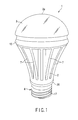
- FIGS. 1 and 2 illustrate a bulb-type LED lamp 1 as an example of an illumination device.
- the LED lamp 1 comprises a lamp body 2, a globe 3, an E-shaped base 4, a lighting device 5, and a chip-on-board (COB) light-emitting device 6.
- COB chip-on-board
- the lamp body 2 is made of a metallic material having excellent thermal conductivity, such as aluminum, and also functions as a thermally radiative member.
- the lamp body 2 has a substantially round columnar shape.
- a plurality of thermally radiative fins 7 is formed to be integral with an outer circumferential surface of the lamp body 2.
- the thermally radiative fins 7 protrude from the outer circumferential surface of the lamp body 2, and taper outward radially from the lamp body 2 from one end of the body to the other.
- the lamp body 2 is formed to have a greater diameter at the other end thereof than at the one end thereof.
- the lamp body 2 comprises a first recess 8 and a second recess 9.
- the first recess 8 is located at one end of the lamp body 2, and extends toward the other end of the lamp body 2.
- the second recess 9 is located at the other end of the lamp body 2, and extends toward the end of the lamp body 2 at which the first recess 8 is located.
- the second recess 9 has a bottom which is a flat support surface 9a.
- an annular step part 10 is provided at the other end of the lamp body 2. The step part 10 surrounds the second recess 9 and is open to periphery of the lamp body 2.
- the globe 3 is, for example, formed in a substantially semi-spherical shape from optically diffusive glass or a composite resin material.
- the globe 3 has a spherical top 3a and an opening 11 opposed to the top 3a.
- the opening 11 has a smaller diameter than a maximum diameter of the globe 3.
- An edge part 11a of the globe 3 which defines the opening 11 is protruded to a side opposite to the top 3a of the globe 3, and is engaged with the second recess 9 of the lamp body 2.
- the globe 3 is joined to the lamp body 2, and covers the support surface 9a of the second recess 9.
- the step part 10 positioned at the other end of the lamp body 2 is adjacent to an outer circumferential part of such a part of the globe 3 that has a maximum diameter.
- a reflection ring 12 is attached to the step part 10.
- the reflection ring 12 connects an outer circumferential edge of the other end of the lamp body 2 with an outer circumferential part of the globe 3.
- a cover member 14 is attached to the first recess 8 of the lamp body 2.
- the cover member 14 may be made of an electrically insulative material, such as PET resin.
- the cover member 14 comprises a cylindrical circumferential wall 14a and an end wall 14b.
- the circumferential wall 14a is engaged with the first recess 8 and covers an inner circumferential surface of the first recess 8.
- the circumferential wall 14a comprises a cylindrical protrusion 15 which protrudes out of the lamp body 2 from the first recess 8.
- the end wall 14b closes an opening end of the circumferential wall 14a, and covers a bottom of the first recess 8. Further, an internal space of the cover member 14 communicates with the support surface 9a of the lamp body 2 through a through hole 16 which penetrates the lamp body 2.
- the base 4 is constituted by a metal shell 17 screwed into a lamp socket, and an insulator 19 including an eyelet terminal 18.
- the shell 17 is attached to the protrusion 15 so as to cover the protrusion 15 of the cover member 14 from outside.
- the insulator 19 collides with an opening end of the protrusion 15, and closes the internal space of the cover member 14.
- the cover member 14 comprises a flange 20 which extends from an outer circumferential surface of the protrusion 15.
- the flange 20 is provided to continue in a circumferential direction of the protrusion 15.
- the flange 20 is provided between an open end of the shell 17 and the one end of the lamp body 2, and electrically insulates the base 4 and the lamp body 2 from each other.
- the lighting device 5 is contained in the internal space of the cover member 14, and is electrically connected to the base 4.
- the lighting device 5 comprises a rectangular circuit board 22 and a plurality of such circuit components 23 as a transistor, resistor, constant voltage diode, full-wave rectifier, and capacitor mounted on the circuit board 22.
- the circuit board 22 is provided inside the cover member 14, oriented vertically along the axis of the lamp body 2.
- the region bounded by the cover member 14 is not limited to being a space for merely containing the lighting device 5.
- a filler which has thermally radiative characteristics and provides electrical insulation may be introduced into the space bounded by the cover member 14.
- a silicone-based resin material may be used as the filler. The filler is inserted between the lighting device 5 and the cover member 14 so as to cover the lighting device 5.
- the light-emitting device 6 is used as a light source for the LED lamp 1.
- the light-emitting device 6 is attached to the support surface 9a of the lamp body 2, and covers the globe 3.
- light-emitting device 6 comprises a rectangular substrate 25.
- the substrate 25 is made of, for example, a white ceramic material such as aluminum oxide or aluminum nitride, and is electrically insulative.
- the substrate 25 has a first surface 25a, a second surface 25b, and an outer circumferential surface 25c.
- the first surface 25a is a flat surface facing the support surface 9a of the lamp body 2.
- the second surface 25b is positioned in a side opposite to the first surface 25a, and constitutes a flat mounting surface.
- the outer circumferential surface 25c bridges outer circumferential edges of the first surface 25a and second surface 25b, and extends in the thickness direction of the substrate 25.
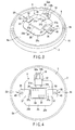
- the second surface 25b of the substrate 25 includes a rectangular mounting area 26 as illustrated in FIGS. 4 and 8 .
- the mounting area 26 is positioned in the center of the second surface 25b.
- a plurality of wire patterns 27 are formed on the mounting area 26.
- the wire patterns 27 are arrayed in a matrix at intervals between each other.
- a plurality of light-emitting diode chips 28 are provided on the mounting area 26.
- the first embodiment uses about 100 light-emitting diode chips 28.
- the light-emitting diode chips 28 are each bonded to the mounting area 26 with a silicone-based adhesive agent, and are regularly arranged to be adjacent to the wire patterns 27, respectively.
- the first embodiment uses, for example, InGaN light-emitting elements as the light-emitting diode chips 28.
- the light-emitting diode chips 28 each comprise a translucent sapphire board, and a light-emitting layer which is layered on the sapphire board and emits blue light.
- the light-emitting layer is constituted by layering an N-type nitride semiconductor layer, an InGaN light-emitting layer, and a P-type nitride semiconductor layer on one another.
- the light-emitting diode chips 28 each comprise positive and negative electrodes which supply the light-emitting layer with an electric current.
- the positive electrode comprises a P-type electrode pad formed on the P-type nitride semiconductor layer.
- the negative electrode comprises an N-type electrode pad formed on the N-type nitride semiconductor layer.
- the positive and negative electrodes each are electrically connected to an adjacent one of the wire patterns 27 through a bonding wire 29.
- the first embodiment uses a gold wire as the bonding wire 29.
- the bonding wires 29 are connected to the positive and negative electrodes and the wire patterns 27 through bumps containing Au as a main component, respectively.
- the wire patterns 27 and light-emitting diode chips 28 are covered with a sealing material 30.
- the sealing material 30 is made of, for example, a transparent or translucent resin material having optical permeability, such as epoxy resin or silicone resin.
- the sealing material 30 contains a fluorescent substance.
- As the fluorescent substance a yellow fluorescent substance which emits yellow light when excited by blue light emitted by the light-emitting diode chips 28 is used.
- a pair of power supply terminals 31a and 31b are provided on the second surface 25b of the substrate 25.
- the power supply terminals 31a and 31b are provided at positions apart from the mounting area 26, and are electrically connected to the wire patterns 27.
- a connector 32 is soldered to the power supply terminals 31a and 31b.
- the connector 32 is electrically connected to the lighting device 5 through covered cables 32a and 32b which are inserted in the through hole 16.
- a pair of pressure members 33 and 34 is attached to the support surface 9a of the lamp body 2.
- the pressure members 33 and 34 elastically support the light-emitting device 6 on the support surface 9a of the lamp body 2, at two portions with the mounting area 26 of the substrate 25 positioned therebetween.
- the pressure members 33 and 34 have a configuration common to each other, and therefore, only pressure member 33 will be described as a representative.
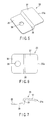
- the pressure member 33 is constituted by a plate spring which is formed, for example, by folding a stainless steel plate having a thickness of 0.3 mm into steps. More specifically, as illustrated in FIGS. 5 to 7 , the pressure member 33 comprises a fixing part 35, a rising part 36, and a pressure part 37.
- the fixing part 35 has a flat rectangular shape, and has an insertion hole 38 at the center thereof.
- the rising part 36 substantially vertically rises from the edge of the fixing part 35.
- the rising part 36 has a greater height than the substrate 25.
- the pressure part 37 is a flat rectangular plate-like shape, and extends from a protruding end of the rising part 36 toward an opposite side to the fixing part 35. Further, the pressure part 37 is inclined downwards from the rising part 36 and is elastically deformable about the protruding end of the rising part 36 as a fulcrum.
- the fixing part 35 of the pressure member 33 is fixed to the support surface 9a of the lamp body 2 by a screw 40.
- the screw 40 penetrates the insertion hole 38 of the fixing part 35 and is driven into a screw hole 41 provided in the support surface 9a.
- the rising part 36 of the pressure member 33 faces the outer circumferential surface 25c of the substrate 25, and the pressure part 37 of the pressure member 33 extends over an outer peripheral part of the second surface 25b of the substrate 25.
- a top end 37a of the pressure part 37 makes elastic contact with the second surface 25b of the substrate 25.
- the pressure part 37 applies a load to the substrate 25, which elastically presses the first surface 25a of the substrate 25 toward the support surface 9a.
- the first surface 25a of the substrate 25 is pressed against the support surface 9a, and the light-emitting device 6 is elastically maintained on the lamp body 2.
- the substrate 25 of the light-emitting device 6 is thermally connected to the support surface 9a of the lamp body 2.
- thermally conductive grease is desirably introduced between the first surface 25a of the substrate 25 and the support surface 9a of the lamp body 2, to ensure a more reliable thermal path between the substrate 25 and the lamp body 2.
- the rising part 36 bridging the fixing part 35 and the pressure part 37 is apart from the outer circumferential surface 25c of the substrate 25 when the pressure member 33 is fixed to the support surface 9a.
- a gap of, for example, about 0.5 mm is created between the rising part 36 of the pressure member 33 and the outer circumferential surface 25c of the substrate 25.
- the gap g functions as, namely, a play which allows the pressure member 33 fixed to the support surface 9a and the substrate 25 to move relatively to each other.
- the LED lamp 1 As described above, a voltage is applied to the light-emitting device 6 through the lighting device 5. As a result, all the light-emitting diode chips 28 on the substrate 25 emit light at once. The blue light emitted by the light-emitting diode chips 28 is incident on the sealing material 30. A part of the blue light incident on the sealing material 30 is absorbed by the yellow fluorescent substance. The remaining blue light is not absorbed by the yellow fluorescent substance but penetrates the sealing material 30.
- the yellow fluorescent substance which has absorbed the blue light is excited and emits yellow light.
- the yellow light penetrates the sealing material 30.
- the yellow light and the blue light are mixed with each other into white light inside the sealing material 30.
- the white light is radiated toward the globe 3 from the sealing material 30, and penetrates the globe 3 for an illumination purpose. Light which penetrates the part of the globe 3 having the maximum diameter toward the lamp body 2 is reflected by the reflection ring 12 and is guided in a direction in which the light is to be output.
- the thermal radiation performance of the light-emitting diode chips 28 improves, and overheating of the light-emitting diode chips 28 is suppressed. Accordingly, light-emitting efficiency can be excellently maintained.
- the ceramic substrate 25, lamp body 2, and pressure members 33 and 34 are heated by heat produced by the light-emitting diode chips 28. Then, stress which acts on the substrate 25 supported on the support surface 9a can be produced in the thickness direction of the substrate 25 and along the support surface 9a since there appear differences in coefficient of thermal expansion between the substrate 25, lamp body 2, and pressure members 33 and 34.
- the pressure parts 37 of the pressure members 33 and 34 which press the substrate 25 against the support surface 9a are elastically deformable in the thickness direction of the substrate 25.
- the stress along the thickness direction of the substrate 25 can be absorbed by elasticity of the pressure parts 37.
- the rising parts 36 of the pressure members 33 and 34 are apart from the outer circumferential surface 25c of the substrate 25, and the gap g is maintained between the rising part 36 and the outer circumferential surface 25c of the substrate 25.
- the gap g allows play to absorb the stress acting on the substrate 25.
- the inventor conducted a test for investigating the thermal resistance ratio between the substrate 25 and the support surface 9a, and the rate at which the substrate 25 cracks when the load applied to the substrate 25 by the pressure members 33 and 34 is changed.
- This test involved a ceramic substrate containing 96% alumina, and stainless steel pressure members 33 and 34. After 40,000 hours of operation, the ratio of change of elasticity of the stainless steel was 88% with the pressure members 33 and 34 at a temperature of 90°C, 84% at 120°C, and 78% at 150°C.
- test sample 1 The test was conducted on an LED lamp according to the prior art in which a substrate was perfectly fixed to a support surface by screws, and on an LED lamp according to test samples 1 to 5, below, in which substrates were elastically supported on support surfaces.
- the load elastically applied to the substrate was 150 g; for test sample 2, 200 g; for test sample 3, 250 g; for test sample 4, 300 g; and for test sample 5, 350 g.
- Table 1 shows the results of investigating the thermal resistance ratio and the rate at which the substrate cracks in each of the prior art and test samples 1 to 5.
- the thermal resistance ratios were evaluated relative to the thermal resistance ratio of the prior art sample as 100%.
- Table 1 Prior Art Test Sample 1 Test Sample 2
- Test Sample 3 Test Sample 4
- Test Sample 5 Support method Screw Elastic support Elastic support Elastic support Elastic support Load (g) Perfectly fixed 150 200 250 300 350 Thermal resistance ratio (%) 100 140 120 110 100 90 Cracking probability (%) 20 0 0 0 0 10
- the probability of the substrate cracking was 20% for the prior art sample.
- the thermal resistance ratio decreased as the load applied to the substrate increased. Thermal conduction from the substrate to the lamp body was found to be excellent.
- the probability of the substrate cracking was found to be 10%.
- the load applied to the substrate is desirably set to 200 to 300 g to achieve excellent thermal conduction from the substrate to the lamp body. Furthermore, with such a load, cracking of the substrate can be eliminated. Thus, the substrate can be relied on to remain stable on the support surface of the lamp body.
- FIG. 9 illustrates the second embodiment.
- the second embodiment differs from the first in a configuration of pressure members 33 and 34 which apply a load to a substrate of a light-emitting device.
- the configuration of the second embodiment is the same as the first except for the pressure members 33 and 34.
- the pressure members 33 and 34 each comprise a fixing part 50 as a common constitutive element.
- the fixing part 50 is a rectangular frame and comprises first, second, third, and fourth edges 50a, 50b, 50c, and 50.
- the first edge 50a and third edge 50c are arranged parallel to each other with an interval therebetween.
- the second edge 50b and fourth edge 50d are arranged parallel to each other with an interval therebetween. Therefore, the fixing part 50 is placed on a support surface 9a of a lamp body 2 in such a manner that the first, second, third, and fourth edges 50a, 50b, 50c, and 50d surround a substrate 25 of the light-emitting device 6.
- a rising part 36 and a pressure part 37 of one pressure member 33 are formed to be integral with the first edge 50a.
- the pressure part 37 extends from the center of the first edge 50a toward the third edge 50c.
- the first edge 50a comprises an insertion hole 51a at a position corresponding to the one pressure member 33.
- a rising part 36 and a pressure part 37 of the other pressure member 34 are formed to be integral with the third edge 50c.
- the pressure part 37 extends from the center of the third edge 50c toward the first edge 50a.
- the third edge 50c comprises an insertion hole 51b at a position corresponding to the other pressure member 34.
- the fixing part 50 is fixed to the support surface 9a by driving screws into the support surface 9a through the insertion hole 51a and 51b.
- a gap is created between the first, second, third, and fourth edges 50a, 50b, 50c, and 50d of the fixing part 50 and an outer circumferential surface 25c of the substrate 25.
- a pair of pressure members 33 and 34 is connected to each other by the fixing part 50. Therefore, the pair of pressure members 33 and 34 can be simultaneously attached to the support surface 9a of the lamp body 2. Accordingly, assembly work is facilitated.
- the pair of pressure members 33 and 34 form an integral structure, and therefore, management of components can be simplified.
- FIGS. 10 and 11 illustrate the third embodiment.
- the third embodiment differs from the first in that pressure members 33 and 34 also function as a connector for electrical conduction.
- a lamp body 2 and a light-emitting device 6 have the same basic configuration as in the first embodiment. Therefore, parts of the third embodiment that are the same as those of the first are denoted by the same reference symbols, and descriptions thereof are omitted.
- a pair of power supply terminals 31a and 31b is provided on the second surface 25b of the substrate 25 so as to interpose a mounting area 26 between the terminals.
- the power supply terminals 31a and 31b are exposed over the second surface 25b of the substrate 25 at positions corresponding to pressure parts 37 of the pressure members 33 and 34.
- the power supply terminals 31a and 31b are desirably covered with a metal plating layer.
- top edges 37a of the pressure parts 37 make elastic contact with the power supply terminals 31a and 31b. Therefore, the pressure members 33 and 34 apply a load which elastically presses a first surface 25a of the substrate 25 toward a support surface 9a from the power supply terminals 31a and 31b.
- a pair of leads 61a and 61b are connected to fixing parts 35 of the pressure members 33 and 34 by screws 40.
- the leads 61a and 61b are guided into a base through a pair of through holes 62a and 62b opened in the support surface 9a of the lamp body 2, and are electrically connected to a lighting device.
- phosphor bronze copper which has higher electrical conductivity than stainless steel is used, and a surface of the phosphor bronze copper is desirably covered with a metal plating layer, like the power supply terminals 31a and 31b.
- a metal plating layer like the power supply terminals 31a and 31b.
- surfaces of the power supply terminals 31a and 31b are plated with silver
- surfaces of phosphor bronze copper forming the pressure members 33 and 34 may also be plated with silver as well.
- the inventor inspected contact states between the pressure parts 37 of the pressure members 33 and 34 and the power supply terminals 31a and 31b while changing the load applied to the power supply terminals 31a and 31b by the pressure members 33 and 34. Specifically, the load applied to the power supply terminals 31a and 31b by the pressure parts 37 was incremented from 50 to 200 g. When the load was 50, 70, 100, 150, and 200 g, an investigation was made on contact states between the pressure parts 37 and the power supply terminals 31a and 31b.
- the load applied to the power supply terminals 31a and 31b by the pressure parts 37 was concluded to be desirably set to 70 to 200 g in order to appropriately maintain a contact state between the pressure parts 37 of the pressure members 33 and 34 and the power supply terminals 31a and 31b.
- the load applied to the power supply terminals 31a and 31b by the pressure parts 37 is desirably 200 to 300 g.
- the contact pressure between the pressure parts 37 and the power supply terminals 31a and 31b can be sufficiently ensured to counteract vibration applied to the light-emitting device 6. Therefore, the substrate 25 can be securely held on the support surface 9a of the lamp body 2 while adding a function as a contact point to the pressure members 33 and 34.
- the light-emitting device 6 is not thermally influenced by the heat of soldering and can be operated at a junction temperature sustainable by the light-emitting diode chips 28.
- FIGS. 12 and 13 illustrate the fourth embodiment.
- the fourth embodiment differs from the third in that a substrate 25 of a light-emitting device 6 is configured to be held on a support surface 9a of a lamp body 2.
- the lamp body 2 and light-emitting device 6 have the same basic configuration as in the first embodiment. Therefore, parts of the fourth embodiment that are the same as those of the third are denoted by the same reference symbols, and descriptions thereof are omitted.
- a pair of power supply terminals 31a and 31b is guided from a mounting area 26 of a substrate 25 so as to be positioned on a diagonal line of the substrate 25.
- the power supply terminals 31a and 31b extend from the mounting area 26 on the substrate 25 in respectively opposite directions toward two corners of the substrate 25 which face each other.
- a pair of pressure members 71 and 72 is attached to the support surface 9a of the lamp body 2.
- the pressure members 71 and 72 elastically support the light-emitting device 6 on the support surface 9 of the lamp body 2, at positions corresponding to the power supply terminals 31a and 31b.
- the pressure members 71 and 72 have a configuration common to each other, and therefore, only the pressure member 71 will be described as a representative.
- the pressure member 71 comprises a holder 73 made of synthetic resin, and a contact element 74 supported inside the holder 73.
- the holder 73 comprises a fixing part 73a fixed to the support surface 9a of the lamp body 2, and an extension part 73b which extends over a corner of the substrate 25 from a top end of the fixing part 73a.
- the extension part 73b faces the second surface 25b of the substrate 25 and the power supply terminal 31a.
- the contact element 74 is formed of, for example, phosphor bronze copper or a Corson alloy.
- the contact element 74 is electrically connected to the lighting device through a lead 75. Further, the contact element 74 comprises an elastically deformable top end 76. The top end 76 overhangs from the extension 73b of the holder 73 toward the substrate 25 and makes elastic contact with the power supply terminal 31a.
- the contact element 74 applies a load which elastically presses a first surface 25a of the substrate 25 toward the support surface 9a from the power supply terminal 31a. In this way, the light-emitting device 6 is elastically held by the lamp body 2, and the contact element 74 is electrically connected to the power supply terminal 31a.
- the fixing part 73a of the holder 73 is apart from an outer circumferential surface 25c of the substrate 25. Therefore, a gap g is maintained between the fixing part 73a and the outer circumferential surface 25c of the substrate 25.
- the load applied to the power supply terminal 31a by the contact element 74 is desirably set to 70 to 200 g as in the third embodiment.
- the load applied to the power supply terminal 31a by the contact element 74 may be set to 200 to 300 g. According to the configuration described above, the substrate 25 can be securely held on the support surface 9a of the lamp body 2, while the contact element 74 of the pressure member 71 is added with a function as a contact point.
- the power supply terminals 31a and 31b extend respectively to a pair of corners facing each other, from the mounting area 26 at the center of the substrate 25.
- the power supply terminals 31a and 31b are positioned on a diagonal line of the substrate 25 with the mounting area 26 interposed between terminals. Therefore, an insulating distance can be sufficiently maintained between the power supply terminals 31a and 31b. Therefore, migration can be prevented from occurring, and deterioration of insulation of the substrate 25 can be avoided.
- FIGS. 14 and 15 illustrate the fifth embodiment.
- a light-emitting device 6 is held on a support surface 9a of a lamp body 2 by a pressure member 33 and a connector member 80.
- the lamp body 2, light-emitting device 6, and pressure member 33 have the same basic configuration as in the first embodiment. Therefore, parts of the fifth embodiment that are the same as those of the first are denoted by the same reference symbols, and descriptions thereof are omitted.
- a pair of power supply terminals 31a and 31b is guided from a mounting area 26 at the center of a substrate 25 toward a side opposite to the pressure member 33. Therefore, the power supply terminals 31a and 31b are arranged parallel to each other to be guided from an outer circumferential part of a second surface 25b of the substrate 25.
- the connector member 80 is attached to the substrate 25 at a position corresponding to the power supply terminals 31a and 31b. As illustrated in FIG. 15 , the connector member 80 comprises a holder 81 made of synthetic resin, and a pair of contact elements 82 (only one of which is illustrated) supported on the holder 81.
- the holder 81 comprises a leg part 83 and a recess 84.
- the leg part 83 is engaged with an engagement aperture 85 from above the support surface 9a, the engagement aperture being opened in the support surface 9a.
- the recess 84 is formed in a peripheral surface of the holder 81 to accept an outer circumferential part of the substrate 25.
- Each of the contact elements 82 is formed of, for example, phosphor bronze copper or a Corson alloy.
- the contact elements 82 are arranged parallel to each other with an interval therebetween, and are electrically connected to a lighting device through leads 86, respectively.
- Each of the contact elements 82 comprises an elastically deformable top end 87.
- the top end 87 hangs to inside of the recess 84 and faces a bottom surface 84a of the recess 84.
- the connector member 80 is held on a light-emitting device 6 by inserting the outer circumferential part of the substrate 25 into the recess 84 of the holder 81.
- the outer circumferential part of the substrate 25 is inserted into the recess 84, top ends 87 of the contact elements 82 make elastic contact with the power supply terminals 31a and 31b.
- the contact elements 82 are electrically connected to the power supply terminals 31a and 31b. Accordingly, an outer circumferential part of a first surface 25a of the substrate 25 is pressed against the bottom surface 84a of the recess 84, and the substrate 25 is held by the connector member 80.
- an inner circumferential surface 84b of the recess 84 is apart from an outer circumferential surface 25c of the substrate 25. Therefore, a gap g is maintained between the inner circumferential surface 84b of the recess 84 and the outer circumferential surface 25c of the substrate 25.
- the connector member 80 integrated with the substrate 25 is set on the support surface 9a by engaging the leg part 83 with the engagement aperture 85 of the lamp body 2. In this state, a fixing part 35 of the pressure member 33 is fixed to the support surface 9a by a screw 40.
- a top edge 37a of the pressure part 37 makes elastic contact with the second surface 25b of the substrate 25.
- the pressure part 37 applies a load to the substrate 25, which elastically presses the first surface 25a of the substrate 25 toward the support surface 9a. In this way, the first surface 25a of the substrate 25 is pressed against the support surface 9a, and the light-emitting device 6 and the connector member 80 are elastically maintained on the lamp body 2.
- the load which the pressure member 33 applies to the substrate 25 is desirably set to 200 to 300 g as in the first embodiment. Further, the load applied to the power supply terminal 31a by the contact elements 82 of the connector member 80 is desirably set to 70 to 200 g as in the third embodiment. In addition, in a type of illumination device in which vibration is applied to a contact part between the contact elements 82 and the power supply terminal 31a, the load applied to the power supply terminal 31a by the contact elements 82 may be set to 200 to 300 g.
- the contact elements 82 of the connector member 80 can be stably put in contact with the power supply terminal 31a. Further, the substrate 25 of the light-emitting device 6 can be securely held on the support surface 9a of the lamp body 2.
Landscapes
- Engineering & Computer Science (AREA)
- General Engineering & Computer Science (AREA)
- Physics & Mathematics (AREA)
- Microelectronics & Electronic Packaging (AREA)
- Optics & Photonics (AREA)
- Fastening Of Light Sources Or Lamp Holders (AREA)
- Arrangement Of Elements, Cooling, Sealing, Or The Like Of Lighting Devices (AREA)
- Non-Portable Lighting Devices Or Systems Thereof (AREA)
- Led Device Packages (AREA)
Applications Claiming Priority (2)
| Application Number | Priority Date | Filing Date | Title |
|---|---|---|---|
| JP2009212502 | 2009-09-14 | ||
| JP2010172717A JP5601512B2 (ja) | 2009-09-14 | 2010-07-30 | 発光装置および照明装置 |
Publications (2)
| Publication Number | Publication Date |
|---|---|
| EP2295844A2 true EP2295844A2 (de) | 2011-03-16 |
| EP2295844A3 EP2295844A3 (de) | 2013-02-27 |
Family
ID=43384627
Family Applications (1)
| Application Number | Title | Priority Date | Filing Date |
|---|---|---|---|
| EP10009465A Withdrawn EP2295844A3 (de) | 2009-09-14 | 2010-09-10 | Lichtemittierende Vorrichtung und Beleuchtungsvorrichtung |
Country Status (4)
| Country | Link |
|---|---|
| US (1) | US8360606B2 (de) |
| EP (1) | EP2295844A3 (de) |
| JP (1) | JP5601512B2 (de) |
| CN (1) | CN102022640B (de) |
Cited By (12)
| Publication number | Priority date | Publication date | Assignee | Title |
|---|---|---|---|---|
| KR20130016775A (ko) * | 2011-08-09 | 2013-02-19 | 엘지이노텍 주식회사 | 조명 장치 |
| EP2413021A3 (de) * | 2010-07-29 | 2013-04-10 | Toshiba Lighting & Technology Corporation | Lichtemittierende Vorrichtung und Beleuchtungsvorrichtung |
| GB2497283A (en) * | 2011-12-02 | 2013-06-12 | Tzu-Yu Liao | Method for assembling LEDs to a ceramic heat conductive member |
| WO2013150481A1 (en) * | 2012-04-05 | 2013-10-10 | Koninklijke Philips N.V. | Led light structure |
| EP2387115A3 (de) * | 2010-05-11 | 2013-11-06 | Toshiba Lighting & Technology Corporation | Lichtemittierende Vorrichtung und Beleuchtungsvorrichtung |
| WO2013182939A1 (en) * | 2012-06-05 | 2013-12-12 | Koninklijke Philips N.V. | A base for an electrical lamp and a method of assembling a base for an electrical lamp |
| EP2712283A1 (de) * | 2012-09-24 | 2014-03-26 | Toshiba Lighting & Technology Corporation | Lichtemittierende Vorrichtung und Leuchte |
| EP2742277A4 (de) * | 2011-08-09 | 2015-03-25 | Lg Innotek Co Ltd | Beleuchtungsvorrichtung |
| EP2918906A1 (de) * | 2014-03-12 | 2015-09-16 | TE Connectivity Nederland B.V. | Buchsenanordnung und -klemme für eine Klemmenanordnung |
| EP3032170A1 (de) * | 2014-12-08 | 2016-06-15 | Tridonic Jennersdorf GmbH | Befestigungsvorrichtung zur befestigung von led-modulen an befestigungsschienen |
| WO2017068019A1 (de) * | 2015-10-21 | 2017-04-27 | Osram Opto Semiconductors Gmbh | Optoelektronische leuchtvorrichtung |
| US9702530B2 (en) | 2013-03-11 | 2017-07-11 | Philips Lighting Holding B.V. | Base for an electrical lamp and a method of assembling a base for an electrical lamp |
Families Citing this family (58)
| Publication number | Priority date | Publication date | Assignee | Title |
|---|---|---|---|---|
| US7758223B2 (en) | 2005-04-08 | 2010-07-20 | Toshiba Lighting & Technology Corporation | Lamp having outer shell to radiate heat of light source |
| CN101978209A (zh) | 2008-06-27 | 2011-02-16 | 东芝照明技术株式会社 | 发光元件灯以及照明设备 |
| JP5333758B2 (ja) | 2009-02-27 | 2013-11-06 | 東芝ライテック株式会社 | 照明装置および照明器具 |
| JP2011049527A (ja) * | 2009-07-29 | 2011-03-10 | Toshiba Lighting & Technology Corp | Led照明装置 |
| JP5601512B2 (ja) | 2009-09-14 | 2014-10-08 | 東芝ライテック株式会社 | 発光装置および照明装置 |
| JP2011091033A (ja) | 2009-09-25 | 2011-05-06 | Toshiba Lighting & Technology Corp | 発光モジュール、電球形ランプおよび照明器具 |
| CN102032481B (zh) | 2009-09-25 | 2014-01-08 | 东芝照明技术株式会社 | 附带灯口的照明灯及照明器具 |
| US8324789B2 (en) | 2009-09-25 | 2012-12-04 | Toshiba Lighting & Technology Corporation | Self-ballasted lamp and lighting equipment |
| US8678618B2 (en) | 2009-09-25 | 2014-03-25 | Toshiba Lighting & Technology Corporation | Self-ballasted lamp having a light-transmissive member in contact with light emitting elements and lighting equipment incorporating the same |
| JP5469177B2 (ja) * | 2009-09-30 | 2014-04-09 | パナソニック株式会社 | 照明装置 |
| DE102010033092A1 (de) * | 2010-08-02 | 2012-02-02 | Osram Opto Semiconductors Gmbh | Optoelektronisches Leuchtmodul und Kfz-Scheinwerfer |
| JP5677806B2 (ja) * | 2010-11-02 | 2015-02-25 | ローム株式会社 | Led電球 |
| US9091399B2 (en) * | 2010-11-11 | 2015-07-28 | Bridgelux, Inc. | Driver-free light-emitting device |
| US9490235B2 (en) * | 2010-11-22 | 2016-11-08 | Cree, Inc. | Light emitting devices, systems, and methods |
| KR101781424B1 (ko) * | 2010-11-26 | 2017-09-26 | 서울반도체 주식회사 | 엘이디 조명기구 |
| USD693034S1 (en) * | 2011-01-14 | 2013-11-05 | Delta Electronics, Inc. | LED lamp |
| EP2694876A1 (de) * | 2011-04-04 | 2014-02-12 | CeramTec GmbH | Led-lampe mit einer led als leuchtmittel und mit einem lampenschirm aus glas oder kunststoff |
| JP5726616B2 (ja) * | 2011-04-25 | 2015-06-03 | 日本圧着端子製造株式会社 | Led照明用電気的接続装置及びハーネス |
| JP5760185B2 (ja) * | 2011-05-13 | 2015-08-05 | パナソニックIpマネジメント株式会社 | 照明器具 |
| TWM416736U (en) * | 2011-06-03 | 2011-11-21 | Lustrous Technology Ltd | Light guide structure and lamp structure |
| CN103765078A (zh) * | 2011-08-26 | 2014-04-30 | Lg伊诺特有限公司 | 照明装置 |
| US9249955B2 (en) | 2011-09-26 | 2016-02-02 | Ideal Industries, Inc. | Device for securing a source of LED light to a heat sink surface |
| US9429309B2 (en) | 2011-09-26 | 2016-08-30 | Ideal Industries, Inc. | Device for securing a source of LED light to a heat sink surface |
| US9423119B2 (en) | 2011-09-26 | 2016-08-23 | Ideal Industries, Inc. | Device for securing a source of LED light to a heat sink surface |
| DE102011084365A1 (de) * | 2011-10-12 | 2013-04-18 | Osram Gmbh | LED-Modul mit einem Kühlkörper |
| JP5836780B2 (ja) * | 2011-12-02 | 2015-12-24 | 日立アプライアンス株式会社 | 発光ダイオードモジュール及びそれを利用した照明器具 |
| TW201331503A (zh) * | 2012-01-20 | 2013-08-01 | Taiwan Fu Hsing Ind Co Ltd | 燈具結構及其固定座 |
| WO2013112838A1 (en) * | 2012-01-27 | 2013-08-01 | Ideal Industries, Inc. | Device for securing a source of led light to a heat sink surface |
| DE102012202354A1 (de) * | 2012-02-16 | 2013-08-22 | Osram Gmbh | Leuchtmodul |
| JP5879564B2 (ja) * | 2012-02-24 | 2016-03-08 | パナソニックIpマネジメント株式会社 | 発光装置およびそれを用いた照明器具 |
| JP5906436B2 (ja) * | 2012-02-28 | 2016-04-20 | パナソニックIpマネジメント株式会社 | 発光装置およびそれを用いた照明器具 |
| TWI467111B (zh) * | 2012-03-02 | 2015-01-01 | Everlight Electronics Co Ltd | 發光二極體燈具 |
| JP5567616B2 (ja) * | 2012-03-14 | 2014-08-06 | 株式会社セライズ | Led基板の取り付け部材 |
| JP2013201256A (ja) * | 2012-03-23 | 2013-10-03 | Toshiba Lighting & Technology Corp | 配線基板装置、発光モジュール、照明装置および配線基板装置の製造方法 |
| US20130301274A1 (en) * | 2012-05-09 | 2013-11-14 | Deloren E. Anderson | Led fixture with interchangeable components |
| JP5909702B2 (ja) * | 2012-07-31 | 2016-04-27 | パナソニックIpマネジメント株式会社 | 照明器具 |
| JP5895196B2 (ja) * | 2012-07-31 | 2016-03-30 | パナソニックIpマネジメント株式会社 | 照明器具 |
| WO2014024147A1 (en) * | 2012-08-07 | 2014-02-13 | Koninklijke Philips N.V. | Lighting device comprising a heat sink structure |
| JP6150050B2 (ja) * | 2012-12-07 | 2017-06-21 | 東芝ライテック株式会社 | 発光装置及び照明装置 |
| JP6104946B2 (ja) * | 2013-01-24 | 2017-03-29 | シャープ株式会社 | 発光装置およびその製造方法 |
| CN103411181A (zh) * | 2013-07-01 | 2013-11-27 | 广德润视机电有限公司 | 一种用于面板灯上固定led灯装置 |
| JP6191914B2 (ja) | 2013-10-09 | 2017-09-06 | パナソニックIpマネジメント株式会社 | 照明装置 |
| TWI561764B (en) * | 2013-10-24 | 2016-12-11 | Lextar Electronics Corp | Lamp structure |
| JP5605966B1 (ja) * | 2013-11-13 | 2014-10-15 | アイリスオーヤマ株式会社 | Led電球及び照明器具 |
| US9435528B2 (en) * | 2014-04-16 | 2016-09-06 | Cree, Inc. | LED lamp with LED assembly retention member |
| JP6191593B2 (ja) | 2014-12-26 | 2017-09-06 | 東芝ライテック株式会社 | 車両用灯具 |
| US10260718B2 (en) * | 2015-04-30 | 2019-04-16 | Hubbell Incorporated | Area luminaire |
| CN105003856A (zh) * | 2015-08-21 | 2015-10-28 | 江苏翠钻照明有限公司 | 一种易组装的led灯具 |
| US20170175990A1 (en) * | 2015-12-16 | 2017-06-22 | Jitendra Patel | Led array apparatus |
| CN205579174U (zh) * | 2016-01-09 | 2016-09-14 | 深圳市耀嵘科技有限公司 | 替换式led灯具 |
| JP2017130397A (ja) * | 2016-01-22 | 2017-07-27 | 日立アプライアンス株式会社 | 電球形照明装置 |
| TWI582340B (zh) * | 2016-05-13 | 2017-05-11 | 綠點高新科技股份有限公司 | 照明裝置 |
| CN206918825U (zh) * | 2017-04-25 | 2018-01-23 | 漳州立达信光电子科技有限公司 | 一种分体式筒灯 |
| US10203096B2 (en) * | 2017-06-28 | 2019-02-12 | Conservation Technology of Illinois LLC | Powering and fastening a light emitting diode or chip-on-board component to a heatsink |
| JP2019197626A (ja) * | 2018-05-08 | 2019-11-14 | シチズン時計株式会社 | 発光装置 |
| US11168879B2 (en) * | 2020-02-28 | 2021-11-09 | Omachron Intellectual Property Inc. | Light source |
| CN113013114A (zh) * | 2021-02-24 | 2021-06-22 | 同辉电子科技股份有限公司 | 一种新型led芯片 |
| CN114992591B (zh) * | 2021-03-01 | 2024-11-01 | 松下知识产权经营株式会社 | 灯具 |
Family Cites Families (117)
| Publication number | Priority date | Publication date | Assignee | Title |
|---|---|---|---|---|
| US356107A (en) * | 1887-01-18 | Ella b | ||
| US534665A (en) * | 1895-02-26 | Method of casting projectiles | ||
| US534038A (en) * | 1895-02-12 | Dynamo-electric machine | ||
| GB1601461A (en) * | 1977-05-21 | 1981-10-28 | Amp Inc | Electrical junction box |
| JPS57152706A (en) | 1981-03-17 | 1982-09-21 | T C Denshi Kk | Antenna |
| US4503360A (en) | 1982-07-26 | 1985-03-05 | North American Philips Lighting Corporation | Compact fluorescent lamp unit having segregated air-cooling means |
| JPH0617298B2 (ja) | 1984-07-26 | 1994-03-09 | サンスタ−株式会社 | 義歯洗浄剤 |
| JPS62190366A (ja) | 1986-02-13 | 1987-08-20 | 日本水産株式会社 | 合成含気氷ならびにその製造方法 |
| JPS635581A (ja) | 1986-06-25 | 1988-01-11 | Semiconductor Res Found | 抵抗器内装型led表示灯の放熱方法 |
| JPS63102265A (ja) | 1986-10-20 | 1988-05-07 | Agency Of Ind Science & Technol | 半導体装置の製造方法 |
| JPS647204A (en) | 1987-06-30 | 1989-01-11 | Fanuc Ltd | Preparation of nc data for rough working |
| JPH0343609Y2 (de) * | 1987-12-14 | 1991-09-12 | ||
| JPH01206505A (ja) | 1988-02-12 | 1989-08-18 | Toshiba Corp | けい光ランプ装置 |
| JPH0291105A (ja) | 1988-09-28 | 1990-03-30 | Japan Synthetic Rubber Co Ltd | ポリブタジエン |
| USD356107S (en) | 1992-05-15 | 1995-03-07 | Fujitsu Limited | Developing cartridge for copier |
| JP3121916B2 (ja) | 1992-06-25 | 2001-01-09 | 矢橋工業株式会社 | 石灰焼結体の製造方法 |
| US5537301A (en) * | 1994-09-01 | 1996-07-16 | Pacific Scientific Company | Fluorescent lamp heat-dissipating apparatus |
| EP0835408B1 (de) * | 1995-06-29 | 2001-08-22 | Siemens Microelectronics, Inc. | Gezielte beleuchtung unter verwendung der tir-technologie |
| US6095668A (en) * | 1996-06-19 | 2000-08-01 | Radiant Imaging, Inc. | Incandescent visual display system having a shaped reflector |
| US5785418A (en) * | 1996-06-27 | 1998-07-28 | Hochstein; Peter A. | Thermally protected LED array |
| US5857767A (en) * | 1996-09-23 | 1999-01-12 | Relume Corporation | Thermal management system for L.E.D. arrays |
| JP2000083343A (ja) | 1998-09-03 | 2000-03-21 | Mitsubishi Electric Corp | モーターフレーム及びモーターフレームの製造方法 |
| DE69936375T2 (de) | 1998-09-17 | 2008-02-28 | Koninklijke Philips Electronics N.V. | Led-leuchte |
| JP3753291B2 (ja) | 1998-09-30 | 2006-03-08 | 東芝ライテック株式会社 | 電球形蛍光ランプ |
| JP2001243809A (ja) | 2000-02-28 | 2001-09-07 | Mitsubishi Electric Lighting Corp | Led電球 |
| US6814470B2 (en) * | 2000-05-08 | 2004-11-09 | Farlight Llc | Highly efficient LED lamp |
| US6582100B1 (en) * | 2000-08-09 | 2003-06-24 | Relume Corporation | LED mounting system |
| US6517217B1 (en) * | 2000-09-18 | 2003-02-11 | Hwa Hsia Glass Co., Ltd. | Ornamental solar lamp assembly |
| JP2002280617A (ja) | 2001-03-19 | 2002-09-27 | Matsushita Electric Ind Co Ltd | 照明装置 |
| JP4674418B2 (ja) | 2001-06-29 | 2011-04-20 | パナソニック株式会社 | 照明装置 |
| JP4076329B2 (ja) | 2001-08-13 | 2008-04-16 | エイテックス株式会社 | Led電球 |
| JP2003059330A (ja) | 2001-08-16 | 2003-02-28 | Matsushita Electric Works Ltd | Led照明器具 |
| JP2003092022A (ja) | 2001-09-19 | 2003-03-28 | Yamada Shomei Kk | 照明器具の放熱構造及び照明器具 |
| US6942365B2 (en) * | 2002-12-10 | 2005-09-13 | Robert Galli | LED lighting assembly |
| EP1467414A4 (de) * | 2001-12-29 | 2007-07-11 | Hangzhou Fuyang Xinying Dianzi | Led und led-lampe |
| US6936855B1 (en) * | 2002-01-16 | 2005-08-30 | Shane Harrah | Bendable high flux LED array |
| JP2004006096A (ja) | 2002-05-31 | 2004-01-08 | Nippon Seiki Co Ltd | 照明装置 |
| US7188980B2 (en) * | 2002-12-02 | 2007-03-13 | Honda Motor Co., Ltd. | Head light system |
| US7153004B2 (en) * | 2002-12-10 | 2006-12-26 | Galli Robert D | Flashlight housing |
| JP2004193053A (ja) | 2002-12-13 | 2004-07-08 | Toshiba Lighting & Technology Corp | 電球形蛍光ランプおよび照明器具 |
| US6964501B2 (en) | 2002-12-24 | 2005-11-15 | Altman Stage Lighting Co., Ltd. | Peltier-cooled LED lighting assembly |
| JP4038136B2 (ja) | 2003-01-13 | 2008-01-23 | シーシーエス株式会社 | パワーledを利用したスポット照明装置 |
| JP3885032B2 (ja) | 2003-02-28 | 2007-02-21 | 松下電器産業株式会社 | 蛍光ランプ |
| JP4236544B2 (ja) | 2003-09-12 | 2009-03-11 | 三洋電機株式会社 | 照明装置 |
| US6982518B2 (en) * | 2003-10-01 | 2006-01-03 | Enertron, Inc. | Methods and apparatus for an LED light |
| US6942360B2 (en) * | 2003-10-01 | 2005-09-13 | Enertron, Inc. | Methods and apparatus for an LED light engine |
| US7144135B2 (en) * | 2003-11-26 | 2006-12-05 | Philips Lumileds Lighting Company, Llc | LED lamp heat sink |
| JP2005166578A (ja) | 2003-12-05 | 2005-06-23 | Hamai Denkyu Kogyo Kk | 電球形ledランプ |
| US7198387B1 (en) * | 2003-12-18 | 2007-04-03 | B/E Aerospace, Inc. | Light fixture for an LED-based aircraft lighting system |
| JP4343720B2 (ja) * | 2004-01-23 | 2009-10-14 | 株式会社小糸製作所 | 灯具 |
| US6948829B2 (en) * | 2004-01-28 | 2005-09-27 | Dialight Corporation | Light emitting diode (LED) light bulbs |
| JP2005217354A (ja) * | 2004-02-02 | 2005-08-11 | Sumitomo Wiring Syst Ltd | 発光素子ユニット |
| JP2005286267A (ja) | 2004-03-31 | 2005-10-13 | Hitachi Lighting Ltd | 発光ダイオードランプ |
| JP2006040727A (ja) | 2004-07-27 | 2006-02-09 | Matsushita Electric Works Ltd | 発光ダイオード点灯装置及び照明器具 |
| DE102004042186B4 (de) | 2004-08-31 | 2010-07-01 | Osram Opto Semiconductors Gmbh | Optoelektronisches Bauelement |
| US20050218385A1 (en) * | 2004-10-30 | 2005-10-06 | Larry Lemelson | Appliance for safe lifting and method for its use |
| US7165866B2 (en) * | 2004-11-01 | 2007-01-23 | Chia Mao Li | Light enhanced and heat dissipating bulb |
| JP2005123200A (ja) | 2004-11-04 | 2005-05-12 | Toshiba Lighting & Technology Corp | 電球形蛍光ランプ |
| JP2006156187A (ja) | 2004-11-30 | 2006-06-15 | Mitsubishi Electric Corp | Led光源装置及びled電球 |
| JP3787148B1 (ja) | 2005-09-06 | 2006-06-21 | 株式会社未来 | 照明ユニット及び照明装置 |
| US7144140B2 (en) * | 2005-02-25 | 2006-12-05 | Tsung-Ting Sun | Heat dissipating apparatus for lighting utility |
| JP2006244725A (ja) * | 2005-02-28 | 2006-09-14 | Atex Co Ltd | Led照明装置 |
| US7255460B2 (en) | 2005-03-23 | 2007-08-14 | Nuriplan Co., Ltd. | LED illumination lamp |
| JP4379731B2 (ja) * | 2005-04-01 | 2009-12-09 | 住友電装株式会社 | 発光装置 |
| CN100559073C (zh) | 2005-04-08 | 2009-11-11 | 东芝照明技术株式会社 | 灯 |
| JP4725231B2 (ja) | 2005-04-08 | 2011-07-13 | 東芝ライテック株式会社 | 電球型ランプ |
| US7758223B2 (en) | 2005-04-08 | 2010-07-20 | Toshiba Lighting & Technology Corporation | Lamp having outer shell to radiate heat of light source |
| JP4482706B2 (ja) | 2005-04-08 | 2010-06-16 | 東芝ライテック株式会社 | 電球型ランプ |
| USD534665S1 (en) | 2005-04-15 | 2007-01-02 | Toshiba Lighting & Technology Corporation | Light emitting diode lamp |
| US7226189B2 (en) * | 2005-04-15 | 2007-06-05 | Taiwan Oasis Technology Co., Ltd. | Light emitting diode illumination apparatus |
| USD535038S1 (en) | 2005-04-15 | 2007-01-09 | Toshiba Lighting & Technology Corporation | Light emitting diode lamp |
| JP2006310057A (ja) | 2005-04-27 | 2006-11-09 | Arumo Technos Kk | Led照明灯及びled点灯制御回路 |
| US7744256B2 (en) * | 2006-05-22 | 2010-06-29 | Edison Price Lighting, Inc. | LED array wafer lighting fixture |
| ES2376350T3 (es) * | 2005-07-20 | 2012-03-13 | Tbt Asset Management International Limited | Unidad de iluminación con l�?mpara fluorescente de c�?todo fr�?o de forma serpentina. |
| EP1922227A4 (de) * | 2005-09-06 | 2011-03-02 | Lsi Industries Inc | Lineares beleuchtungssystem |
| JP4715422B2 (ja) * | 2005-09-27 | 2011-07-06 | 日亜化学工業株式会社 | 発光装置 |
| JP2007188832A (ja) | 2006-01-16 | 2007-07-26 | Toshiba Lighting & Technology Corp | ランプ |
| JP2007207576A (ja) | 2006-02-01 | 2007-08-16 | Jefcom Kk | Ledランプ |
| JP4535453B2 (ja) * | 2006-03-06 | 2010-09-01 | 株式会社小糸製作所 | 光源モジュール及び車輌用灯具 |
| WO2007128070A1 (en) * | 2006-05-10 | 2007-11-15 | Spa Electrics Pty Ltd | Assembly including a fastening device |
| TWM309051U (en) * | 2006-06-12 | 2007-04-01 | Grand Halo Technology Co Ltd | Light-emitting device |
| JP2008016362A (ja) * | 2006-07-07 | 2008-01-24 | Koito Mfg Co Ltd | 発光モジュール及び車輌用灯具 |
| US7922359B2 (en) | 2006-07-17 | 2011-04-12 | Liquidleds Lighting Corp. | Liquid-filled LED lamp with heat dissipation means |
| US7396146B2 (en) * | 2006-08-09 | 2008-07-08 | Augux Co., Ltd. | Heat dissipating LED signal lamp source structure |
| DE202006017583U1 (de) * | 2006-11-17 | 2008-03-27 | Patent-Treuhand-Gesellschaft für elektrische Glühlampen mbH | Beleuchtungsvorrichtung |
| JP4582087B2 (ja) * | 2006-12-18 | 2010-11-17 | 市光工業株式会社 | 発光ダイオードの固定構造 |
| JP4858204B2 (ja) * | 2007-02-08 | 2012-01-18 | ソニー株式会社 | バックライト装置及び表示装置 |
| US7510400B2 (en) * | 2007-03-14 | 2009-03-31 | Visteon Global Technologies, Inc. | LED interconnect spring clip assembly |
| JP4753904B2 (ja) | 2007-03-15 | 2011-08-24 | シャープ株式会社 | 発光装置 |
| JP2008277561A (ja) | 2007-04-27 | 2008-11-13 | Toshiba Lighting & Technology Corp | 照明装置 |
| JP4980152B2 (ja) * | 2007-06-19 | 2012-07-18 | シャープ株式会社 | 照明装置 |
| US8226270B2 (en) * | 2007-05-23 | 2012-07-24 | Sharp Kabushiki Kaisha | Lighting device |
| FR2922295B1 (fr) * | 2007-10-12 | 2009-12-04 | In Novea | Module d'eclairage comportant plusieurs diodes electroluminescentes et ensemble d'eclairage comprenant un tel module |
| JP4569683B2 (ja) | 2007-10-16 | 2010-10-27 | 東芝ライテック株式会社 | 発光素子ランプ及び照明器具 |
| DE102007055133A1 (de) * | 2007-11-19 | 2009-05-20 | Osram Gesellschaft mit beschränkter Haftung | Beleuchtungsvorrichtung mit einem Kühlkörper |
| JP2009135026A (ja) | 2007-11-30 | 2009-06-18 | Toshiba Lighting & Technology Corp | Led照明器具 |
| US7625104B2 (en) * | 2007-12-13 | 2009-12-01 | Philips Lumileds Lighting Company, Llc | Light emitting diode for mounting to a heat sink |
| US7762829B2 (en) * | 2007-12-27 | 2010-07-27 | Tyco Electronics Corporation | Connector assembly for termination of miniature electronics |
| JP5353216B2 (ja) * | 2008-01-07 | 2013-11-27 | 東芝ライテック株式会社 | Led電球及び照明器具 |
| CN101978209A (zh) | 2008-06-27 | 2011-02-16 | 东芝照明技术株式会社 | 发光元件灯以及照明设备 |
| CN102175000B (zh) | 2008-07-30 | 2013-11-06 | 东芝照明技术株式会社 | 灯装置及照明器具 |
| US7919339B2 (en) * | 2008-09-08 | 2011-04-05 | Iledm Photoelectronics, Inc. | Packaging method for light emitting diode module that includes fabricating frame around substrate |
| DE202008016231U1 (de) | 2008-12-08 | 2009-03-05 | Huang, Tsung-Hsien, Yuan Shan | Wärmeableiter-Modul |
| JP5333758B2 (ja) | 2009-02-27 | 2013-11-06 | 東芝ライテック株式会社 | 照明装置および照明器具 |
| US20100289393A1 (en) | 2009-05-18 | 2010-11-18 | Hok Product Design, Llc | Integrated Recycling System |
| JP5378882B2 (ja) * | 2009-05-27 | 2013-12-25 | パナソニック株式会社 | 発光モジュールおよび照明装置 |
| JP5348410B2 (ja) | 2009-06-30 | 2013-11-20 | 東芝ライテック株式会社 | 口金付ランプおよび照明器具 |
| JP5354191B2 (ja) | 2009-06-30 | 2013-11-27 | 東芝ライテック株式会社 | 電球形ランプおよび照明器具 |
| JP2011049527A (ja) | 2009-07-29 | 2011-03-10 | Toshiba Lighting & Technology Corp | Led照明装置 |
| JP5601512B2 (ja) | 2009-09-14 | 2014-10-08 | 東芝ライテック株式会社 | 発光装置および照明装置 |
| JP2011071242A (ja) | 2009-09-24 | 2011-04-07 | Toshiba Lighting & Technology Corp | 発光装置及び照明装置 |
| JP2011091033A (ja) | 2009-09-25 | 2011-05-06 | Toshiba Lighting & Technology Corp | 発光モジュール、電球形ランプおよび照明器具 |
| US8678618B2 (en) | 2009-09-25 | 2014-03-25 | Toshiba Lighting & Technology Corporation | Self-ballasted lamp having a light-transmissive member in contact with light emitting elements and lighting equipment incorporating the same |
| CN102032481B (zh) | 2009-09-25 | 2014-01-08 | 东芝照明技术株式会社 | 附带灯口的照明灯及照明器具 |
| US8324789B2 (en) | 2009-09-25 | 2012-12-04 | Toshiba Lighting & Technology Corporation | Self-ballasted lamp and lighting equipment |
| US8602593B2 (en) * | 2009-10-15 | 2013-12-10 | Cree, Inc. | Lamp assemblies and methods of making the same |
| JP5257622B2 (ja) | 2010-02-26 | 2013-08-07 | 東芝ライテック株式会社 | 電球形ランプおよび照明器具 |
-
2010
- 2010-07-30 JP JP2010172717A patent/JP5601512B2/ja not_active Expired - Fee Related
- 2010-09-09 CN CN2010102793033A patent/CN102022640B/zh not_active Expired - Fee Related
- 2010-09-10 EP EP10009465A patent/EP2295844A3/de not_active Withdrawn
- 2010-09-13 US US12/880,490 patent/US8360606B2/en not_active Expired - Fee Related
Non-Patent Citations (1)
| Title |
|---|
| None |
Cited By (21)
| Publication number | Priority date | Publication date | Assignee | Title |
|---|---|---|---|---|
| EP2387115A3 (de) * | 2010-05-11 | 2013-11-06 | Toshiba Lighting & Technology Corporation | Lichtemittierende Vorrichtung und Beleuchtungsvorrichtung |
| EP2413021A3 (de) * | 2010-07-29 | 2013-04-10 | Toshiba Lighting & Technology Corporation | Lichtemittierende Vorrichtung und Beleuchtungsvorrichtung |
| US8727568B2 (en) | 2010-07-29 | 2014-05-20 | Toshiba Lighting & Technology Corporation | Light-emitting apparatus and illumination apparatus |
| US9222660B2 (en) | 2011-08-09 | 2015-12-29 | Lg Innotek Co., Ltd. | Lighting device |
| US10006620B2 (en) | 2011-08-09 | 2018-06-26 | Lg Innotek Co., Ltd. | Lighting device |
| KR101868441B1 (ko) * | 2011-08-09 | 2018-06-18 | 엘지이노텍 주식회사 | 조명 장치 |
| EP2742277A4 (de) * | 2011-08-09 | 2015-03-25 | Lg Innotek Co Ltd | Beleuchtungsvorrichtung |
| KR20130016775A (ko) * | 2011-08-09 | 2013-02-19 | 엘지이노텍 주식회사 | 조명 장치 |
| EP3101331A1 (de) * | 2011-08-09 | 2016-12-07 | LG Innotek Co., Ltd. | Beleuchtungsvorrichtung |
| GB2497283A (en) * | 2011-12-02 | 2013-06-12 | Tzu-Yu Liao | Method for assembling LEDs to a ceramic heat conductive member |
| WO2013150481A1 (en) * | 2012-04-05 | 2013-10-10 | Koninklijke Philips N.V. | Led light structure |
| US9644798B2 (en) | 2012-06-05 | 2017-05-09 | Philips Lighting Holding B.V. | Base for an electrical lamp that prevents rotation and a more efficient method of assembling a base for an electrical lamp |
| RU2631419C2 (ru) * | 2012-06-05 | 2017-09-22 | Филипс Лайтинг Холдинг Б.В. | Цоколь для электрической лампы и способ сборки цоколя для электрической лампы |
| WO2013182939A1 (en) * | 2012-06-05 | 2013-12-12 | Koninklijke Philips N.V. | A base for an electrical lamp and a method of assembling a base for an electrical lamp |
| EP2712283A1 (de) * | 2012-09-24 | 2014-03-26 | Toshiba Lighting & Technology Corporation | Lichtemittierende Vorrichtung und Leuchte |
| US9702530B2 (en) | 2013-03-11 | 2017-07-11 | Philips Lighting Holding B.V. | Base for an electrical lamp and a method of assembling a base for an electrical lamp |
| WO2015136010A1 (en) * | 2014-03-12 | 2015-09-17 | Te Connectivity Nederland Bv | Socket assembly and clamp for a socket assembly |
| EP2918906A1 (de) * | 2014-03-12 | 2015-09-16 | TE Connectivity Nederland B.V. | Buchsenanordnung und -klemme für eine Klemmenanordnung |
| US10527260B2 (en) | 2014-03-12 | 2020-01-07 | Te Connectivity Nederland Bv | Socket assembly and clamp for a socket assembly |
| EP3032170A1 (de) * | 2014-12-08 | 2016-06-15 | Tridonic Jennersdorf GmbH | Befestigungsvorrichtung zur befestigung von led-modulen an befestigungsschienen |
| WO2017068019A1 (de) * | 2015-10-21 | 2017-04-27 | Osram Opto Semiconductors Gmbh | Optoelektronische leuchtvorrichtung |
Also Published As
| Publication number | Publication date |
|---|---|
| US20110063842A1 (en) | 2011-03-17 |
| US8360606B2 (en) | 2013-01-29 |
| JP5601512B2 (ja) | 2014-10-08 |
| CN102022640A (zh) | 2011-04-20 |
| EP2295844A3 (de) | 2013-02-27 |
| JP2011082141A (ja) | 2011-04-21 |
| CN102022640B (zh) | 2013-06-26 |
Similar Documents
| Publication | Publication Date | Title |
|---|---|---|
| US8360606B2 (en) | Light-emitting device and illumination device | |
| CN102263095B (zh) | 发光装置以及照明装置 | |
| US8354783B2 (en) | Light-emitting device.having a frame member surrounding light-emitting elements and illumination device utilizing light-emitting device | |
| EP2413021B1 (de) | Lichtemittierende Vorrichtung und Beleuchtungsvorrichtung | |
| CN100472820C (zh) | 发光器件 | |
| US8641232B2 (en) | Light emitting device and illumination apparatus | |
| EP2346307A2 (de) | Beleuchtungsvorrichtung | |
| CN203481265U (zh) | 发光模块以及照明设备 | |
| CN101043809A (zh) | 用于元件或电路的承载体 | |
| CN101313414A (zh) | 发光装置 | |
| JP4204058B2 (ja) | Led照明器具 | |
| JP2006303396A (ja) | 表面実装型発光装置 | |
| CN101476710A (zh) | 发光器件 | |
| CN203300702U (zh) | 发光模块以及照明设备 | |
| JP5054331B2 (ja) | Ledを用いた照明器具 | |
| JP2009088373A (ja) | Ledランプモジュール | |
| JP2010272736A (ja) | 発光装置 | |
| JP4655735B2 (ja) | Ledユニット | |
| JP4944428B2 (ja) | 発光装置 | |
| CN203489203U (zh) | 灯及照明装置 | |
| US10900618B2 (en) | Light-emitting device holder and light source device | |
| JP2012256438A (ja) | 発光装置及び照明装置 | |
| JP2006060050A (ja) | 半導体発光素子の接続装置およびそれを用いた半導体発光装置 |
Legal Events
| Date | Code | Title | Description |
|---|---|---|---|
| PUAI | Public reference made under article 153(3) epc to a published international application that has entered the european phase |
Free format text: ORIGINAL CODE: 0009012 |
|
| 17P | Request for examination filed |
Effective date: 20100910 |
|
| AK | Designated contracting states |
Kind code of ref document: A2 Designated state(s): AL AT BE BG CH CY CZ DE DK EE ES FI FR GB GR HR HU IE IS IT LI LT LU LV MC MK MT NL NO PL PT RO SE SI SK SM TR |
|
| AX | Request for extension of the european patent |
Extension state: BA ME RS |
|
| PUAL | Search report despatched |
Free format text: ORIGINAL CODE: 0009013 |
|
| AK | Designated contracting states |
Kind code of ref document: A3 Designated state(s): AL AT BE BG CH CY CZ DE DK EE ES FI FR GB GR HR HU IE IS IT LI LT LU LV MC MK MT NL NO PL PT RO SE SI SK SM TR |
|
| AX | Request for extension of the european patent |
Extension state: BA ME RS |
|
| RIC1 | Information provided on ipc code assigned before grant |
Ipc: H01L 33/64 20100101ALI20130123BHEP Ipc: H01L 23/40 20060101ALI20130123BHEP Ipc: F21K 99/00 20100101AFI20130123BHEP Ipc: F21V 19/00 20060101ALI20130123BHEP |
|
| 17Q | First examination report despatched |
Effective date: 20130910 |
|
| STAA | Information on the status of an ep patent application or granted ep patent |
Free format text: STATUS: THE APPLICATION IS DEEMED TO BE WITHDRAWN |
|
| 18D | Application deemed to be withdrawn |
Effective date: 20160401 |