EP2296199A2 - Lichtemittierende Halbleitervorrichtung und Herstellungsverfahren davon - Google Patents
Lichtemittierende Halbleitervorrichtung und Herstellungsverfahren davon Download PDFInfo
- Publication number
- EP2296199A2 EP2296199A2 EP10009249A EP10009249A EP2296199A2 EP 2296199 A2 EP2296199 A2 EP 2296199A2 EP 10009249 A EP10009249 A EP 10009249A EP 10009249 A EP10009249 A EP 10009249A EP 2296199 A2 EP2296199 A2 EP 2296199A2
- Authority
- EP
- European Patent Office
- Prior art keywords
- electrode
- layer
- light
- semiconductor layer
- semiconductor
- Prior art date
- Legal status (The legal status is an assumption and is not a legal conclusion. Google has not performed a legal analysis and makes no representation as to the accuracy of the status listed.)
- Granted
Links
Images





Classifications
-
- H—ELECTRICITY
- H10—SEMICONDUCTOR DEVICES; ELECTRIC SOLID-STATE DEVICES NOT OTHERWISE PROVIDED FOR
- H10H—INORGANIC LIGHT-EMITTING SEMICONDUCTOR DEVICES HAVING POTENTIAL BARRIERS
- H10H20/00—Individual inorganic light-emitting semiconductor devices having potential barriers, e.g. light-emitting diodes [LED]
- H10H20/80—Constructional details
- H10H20/81—Bodies
- H10H20/819—Bodies characterised by their shape, e.g. curved or truncated substrates
-
- H—ELECTRICITY
- H10—SEMICONDUCTOR DEVICES; ELECTRIC SOLID-STATE DEVICES NOT OTHERWISE PROVIDED FOR
- H10H—INORGANIC LIGHT-EMITTING SEMICONDUCTOR DEVICES HAVING POTENTIAL BARRIERS
- H10H20/00—Individual inorganic light-emitting semiconductor devices having potential barriers, e.g. light-emitting diodes [LED]
- H10H20/80—Constructional details
- H10H20/83—Electrodes
-
- H—ELECTRICITY
- H10—SEMICONDUCTOR DEVICES; ELECTRIC SOLID-STATE DEVICES NOT OTHERWISE PROVIDED FOR
- H10H—INORGANIC LIGHT-EMITTING SEMICONDUCTOR DEVICES HAVING POTENTIAL BARRIERS
- H10H20/00—Individual inorganic light-emitting semiconductor devices having potential barriers, e.g. light-emitting diodes [LED]
- H10H20/80—Constructional details
- H10H20/83—Electrodes
- H10H20/831—Electrodes characterised by their shape
Definitions
- the present invention relates to a semiconductor light emitting device and particularly to the electrode structure of a light emitting diode (hereinafter referred to as an LED).
- FIGS. 1A and 1B show the structure of a conventional LED chip 100.
- the LED chip 100 has a sapphire substrate 101, an n-layer 102, a light emitting layer 103, a p-layer 104, a transparent electrode 105, an n-electrode 106 formed on the n-layer 102, and a p-electrode 107 formed on the transparent electrode 105. Because the p-layer 104 is lower in conductivity and thinner in film thickness than the n-layer 102, current is difficult to be diffused in planar directions of the LED chip in the p-layer.
- the transparent electrode 105 which makes the current diffuse in planar directions and allows light from the light emitting layer 103 to pass therethrough, is provided on the surface of the p-layer 104.
- a light emission driving current is made to be diffused in planar directions of the LED chip 100, and thus the in-plane uniformity of light emission brightness distribution can be improved.
- the transparent electrode being provided, that effect is not enough, and current concentration and light emission concentration will occur in the peripheries of the p-electrode and the n-electrode and in the vicinity of a straight line joining these electrodes.
- the n-electrode 106 and the p-electrode 107 each have an auxiliary electrode.
- the n-electrode 106 comprises an n-pad portion 106a and comb tooth-shaped n-auxiliary electrodes 106b connected thereto
- the p-electrode 107 includes a p-pad portion 107a and comb tooth-shaped p-auxiliary electrodes 107b connected thereto.
- the n-electrode 106 and the p-electrode 107 are made mainly of metal-based material.
- the areas of both the electrodes are preferably as small as possible, and the auxiliary electrodes are preferably formed to be narrow in width.
- the auxiliary electrodes are shaped like a thin line, heat generation due to the current when the LED is driven increases in amount, resulting in the occurrence of a failure where the p-auxiliary electrode 107b peels off due to stress based on the difference in thermal expansion coefficient between the p-auxiliary electrode 107b and the transparent electrode 105.
- titanium (Ti) is generally used as material for the p-electrode 107 so as to secure adhesion between the transparent electrode 105 made of oxide such as indium tin oxide (ITO) and the p-electrode 107
- titanium (Ti) has the properties of being low in optical reflectivity and likely to absorb light.
- the film thickness of titanium (Ti) needs to be 250 ⁇ (angstroms) or greater, but in this case, the optical reflectivity of the Ti layer surface is greatly reduced to about 50% or less.
- electrode material for the p-electrode is selected giving priority to securing adhesion to the transparent electrode, and hence it is difficult to avoid light absorption by the p-electrode.
- the present invention was made in view of the above facts, and an object thereof is to provide a semiconductor light emitting device that can solve the problem of the auxiliary electrode peeling off and improve light extraction efficiency.
- a semiconductor light emitting device which includes a first semiconductor layer of a first conductivity type (or conduction type); a second semiconductor layer of a second conductivity type different from the first conductivity type; and a light emitting layer provided between the first semiconductor layer and the second semiconductor layer, the semiconductor light emitting device comprises a first electrode formed on the first semiconductor layer; a second electrode formed on the second semiconductor layer; and a light-transmissive electrode covering the second semiconductor layer and the second electrode, wherein contact between the second electrode and the second semiconductor layer is non-ohmic, and the second electrode has a stacked structure including a lower layer and an upper layer whose contact resistance with the light-transmissive electrode is lower than that of the lower layer, part of the second electrode being exposed through an opening formed in the light-transmissive electrode.
- a manufacturing method of a semiconductor light emitting device includes the steps of forming a first semiconductor layer of a first conductivity type on a substrate; forming a light emitting layer on the first semiconductor layer; forming a second semiconductor layer of a second conductivity type different from the first conductivity type on the light emitting layer; making the first semiconductor layer partially exposed; forming a first electrode on the first semiconductor layer; forming a second electrode on the second semiconductor layer such that contact of the second electrode with the second semiconductor layer is non-ohmic; forming a light-transmissive electrode so as to cover the second semiconductor layer and the second electrode; and forming an opening in the light-transmissive electrode so that part of the second electrode is exposed through the opening, wherein the second electrode forming step includes a step of forming on the second semiconductor layer a lower layer made of one material of aluminum, rhodium, and silver, or an alloy of the materials and an upper layer whose contact resistance with the light-transmissive electrode is lower than that
- the semiconductor light emitting device has a configuration where the p-electrode (or n-electrode) is formed directly on the semiconductor film and where the p-electrode (or n-electrode) is covered by a transparent or light-transmissive electrode, and hence the p-electrode (or n-electrode) can be prevented from peeling off. Therefore, electrode material can be selected while taking the optical reflectivity thereof into consideration, thus improving the light extraction efficiency.
- the contact between the p-electrode (or n-electrode) and the semiconductor film is non-ohmic contact (Schottky contact)
- current concentration directly under the p-electrode (or n-electrode) can be prevented, thereby causing the light emission brightness distribution to be uniform.
- FIG. 2A is a perspective view showing the structure of an LED chip 1 that is an embodiment of the present invention
- FIG. 2B is a perspective view including a cross-section taken along line 2b-2b of FIG. 2A
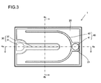
- FIG. 3A is a plan view
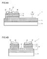
- FIGS. 4A and 4B are respectively cross-sectional views taken along lines 4a-4a and 4b-4b of FIG. 3 .
- An n-electrode 30 is formed on the surface of the n-layer 11 exposed by etching down part of the semiconductor film 14. As shown in FIG.
- the n-electrode has an n-pad portion (hereinafter, simply referred to as n-pad) 31 to be wire-bonded and an n-auxiliary electrode 32 connected to the n-pad 31 and extending along the center line of the LED chip 1.
- the n-auxiliary electrode 32 has the role of diminishing or reducing current concentration when the LED is driven, thereby making the light emission brightness distribution uniform.
- a p-electrode 40 is provided on the surface of the p-layer 13. Specifically, the p-electrode 40 is directly connected to the surface of the p-layer, not onto a transparent or light-transmissive electrode.
- the p-electrode 40 has a p-pad portion (hereinafter, simply referred to as p-pad) 41 to be wire-bonded and a substantially U-shaped p-auxiliary electrode 42 connected to the p-pad 41 and formed surrounding the n-auxiliary electrode 32 substantially.
- the p-auxiliary electrode 42 together with the n-auxiliary electrode 32, has the role of relaxing current concentration when the LED is driven, thereby making the light emission brightness distribution uniform.
- the n-auxiliary electrode 32 and the p-auxiliary electrode 42 are placed such that the distance between both the electrodes is constant across the surface of the LED chip 1.
- the distribution of the light emission driving current flowing between both the electrodes becomes uniform across the surface of the LED chip 1, and thus the light emission brightness distribution can be made uniform.
- the surfaces of the p-electrode 40 and the p-layer 13 are covered by a transparent or light-transmissive electrode 20 made of, e.g., indium tin oxide (ITO).
- the light-transmissive electrode 20 is provided with an opening 21.
- the p-pad 41 is partially exposed through the opening 21, and can be wire-bonded.
- the p-pad 41 and the thin line-shaped p-auxiliary electrode 42 are formed directly on the semiconductor film 14 that is more likely to secure adhesion to them as compared with ITO, and are covered by the light-transmissive electrode 20 except the opening 21. Hence, they are unlikely to peel off even with thermal stress applied thereto.
- FIG. 5 is an enlarged cross-sectional view of the portion where the p-auxiliary electrode 42 is formed.
- the p-electrode 40 can be of multilayer structure.
- a lower layer 401 of the p-auxiliary electrode 42 and the p-pad 41 contacting with the semiconductor film 14 is preferably made of any of aluminum (Al), rhodium (Rh), and silver (Ag), which are relatively high in optical reflectivity, or an alloy including these materials.
- An increase in the optical reflectivity of the lower layer 401 in contact with the semiconductor film 14 causes the amount of light absorbed by the p-electrode 40 to decrease, thus improving the light extraction efficiency.
- the p-electrode 40 is covered by the light-transmissive electrode 20, and its adhesion to the semiconductor film 14 is secured. Hence, material selection can be made giving priority to the optical reflectivity.
- the contact between the lower layer 401 and the semiconductor film 14 is preferably non-ohmic contact (or Schottky contact).
- non-ohmic contact or Schottky contact.
- the lower layer 401 may contain a very small amount of titanium (Ti) or nickel (Ni). Note that if the lower layer 401 contains titanium (Ti) or nickel (Ni), the thickness of the Ti or Ni layer is preferably 10 ⁇ (angstroms) or less so as to suppress a decrease in the optical reflectivity as much as possible.
- a middle layer 402 of titanium (Ti), nickel (Ni), or the like may be provided on the lower layer 401.
- Ti titanium
- Ni nickel
- the adhesion between the light-transmissive electrode 20 and the p-electrode 40 is improved.
- the total film thickness of the p-electrode 40 increases by providing the middle layer 402, and thus the sheet resistance of the thin line-shaped p-auxiliary electrode 42 decreases, resulting in current being likely to spread to the end portions of the p-auxiliary electrode 42.
- gold (Au) is preferably used as the material of the upper layer 403.
- the p-electrode 40 were a single layer of a single material, current flowing out of the p-electrode would immediately flow into the p-layer 13 without being spread widely in the light-transmissive electrode 20, and as a result, the current would be concentrated in the vicinity of the p-electrode 40, making it difficult to achieve a uniform light emission brightness distribution.
- the film thickness of the p-electrode 40 becomes greater, the current path (width "A" in FIG. 5 ) in a thickness direction of the light-transmissive electrode 20 becomes wider.
- the film thickness of the p-electrode 40 becomes greater, the effective sheet resistance of the light-transmissive electrode becomes lower, which can enhance current diffusion in the light-transmissive electrode 20.
- the film thickness of the p-electrode is preferably set at 3,000 ⁇ (angstroms) or less.
- the film thickness of the p-electrode 40 can be set at any value by adjusting mainly the film thicknesses of the middle layer 402 and the upper layer 403.
- Making the p-electrode 40 has a stacked or layered structure formed of materials as described above, improves the light extraction efficiency of the LED chip 1, and in addition enhances current diffusion in the light-transmissive electrode 20, and thus a uniform light emission brightness distribution can be obtained.
- FIGS. 6A to 6D are cross-sectional views for respective process steps showing the manufacturing method of the LED chip 1.
- the n-layer 11, the light emitting layer 12, and the p-layer 13, which are made of Al x In y Ga z N are sequentially grown on the growth substrate 10 by a metal organic chemical vapor deposition (MOCVD) method to form the semiconductor film 14 ( FIG. 6A ).
- MOCVD metal organic chemical vapor deposition
- the sapphire substrate 10 is put into a MOCVD apparatus and heated in a hydrogen atmosphere at about 1,000°C for about 10 minutes (for thermal cleaning).
- the atmosphere or ambient temperature is adjusted to about 500°C, and trimethylgallium (TMG) at a flow rate of 10.4 ⁇ mol/min and ammonia (NH 3 ) at a flow rate of 3.3 LM are supplied for 3 minutes, thereby forming a low-temperature buffer layer of GaN (not shown).
- TMG trimethylgallium
- NH 3 ammonia
- the ambient temperature is raised to 1,000°C, and this state is maintained for 30 seconds to crystallize the low-temperature buffer layer.
- trimethylgallium (TMG) at a flow rate of 45 ⁇ mol/min and ammonia (NH 3 ) at a flow rate of 4.4 LM are supplied for 20 minutes, thereby forming an underlying GaN layer (not shown) of about 1 ⁇ m thickness.
- trimethylgallium (TMG) at a flow rate of 45 ⁇ mol/min, ammonia (NH 3 ) at a flow rate of 4.4 LM, and silane (SiH 4 ) at a flow rate of 2.7 ⁇ 10 -9 ⁇ mol/min are supplied for 60 minutes, thereby growing an n-layer 11 of GaN of about 4 ⁇ m thickness.
- a multi-quantum well structure of InGaN/GaN is applied to the light emitting layer 12.
- an InGaN well layer and a GaN barrier layer as a period, growth of five periods of quantum wells is performed.
- TMG trimethylgallium
- TMI trimethylindium
- NH 3 ammonia
- TMG trimethylgallium
- NH 3 ammonia
- TMG trimethylgallium
- TMA trimethylaluminum
- NH 3 ammonia
- CP2Mg bis-cyclopentadienyl Mg
- TMG trimethylgallium
- NH 3 ammonia
- CP2Mg CP2Mg
- part of the n-layer 11 is exposed by etching down part of the semiconductor film 14 where an n-electrode 30 is to be formed ( FIG. 6B ).
- a photoresist is coated over the surface of the p-layer 13, and patterning of the photo resist is performed by photolithography to form a resist mask.
- the substrate is put into a reactive ion etching (RIE) apparatus, and part of the semiconductor film 14 exposed through the resist mask is etched to make the n-layer 11 partially exposed.
- RIE reactive ion etching
- the n-electrode 30 and the p-electrode 40 are formed respectively on the surface of the p-layer 13 and the surface part exposed in the preceding etching step of the n-layer 11 by a lift-off method ( FIG. 6C ). Specifically, resist masks having desired patterns are formed on the surfaces of the n-layer 11 and the p-layer 13. Then, for the n-electrode 30, a titanium (Ti) film of about 10 ⁇ thickness and an aluminum (A1) film of about 10,000 ⁇ thickness are sequentially formed by electron beam evaporation, then, the n-pad 31 and the n-auxiliary electrode 32 are formed in a pattern by removing (i.e., lifting off) the resist mask together with the electrode materials.
- Ti titanium
- A1 aluminum
- an aluminum (Al) film of about 100 ⁇ thickness and a rhodium (Rh) film of about 1,000 ⁇ thickness are formed by electron beam evaporation to form the lower layer 401.
- a gold (Au) film of about 30 ⁇ thickness is formed to form the upper layer 403.
- the p-pad 41 and the p-auxiliary electrode 42 are formed in a pattern.
- the n-auxiliary electrode 32 and the p-auxiliary electrode 42 are formed in such shapes that the distance between the two is constant at any place in the chip surface.
- the film thickness of the lower layer 401 is preferably 500 ⁇ or greater, more preferably 1,000 ⁇ or greater.
- aluminum (A1) is deposited on the p-layer 13
- rhodium (Rh) is deposited on the aluminum (Al) to form the lower layer 401 in order to make the contact between the p-layer 13 and the p-electrode 40 non-ohmic.
- the film thickness of the Ti layer is preferably 10 ⁇ or less taking the influence on the optical reflectivity into consideration.
- a middle layer 402 of titanium (Ti) or the like may be formed between the lower layer 401 and the upper layer 403 in order to improve the adhesion between the p-electrode 40 and the light-transmissive electrode 20 and in addition enhance current diffusion in the light-transmissive electrode 20.
- the film thickness of the p-electrode is too large, thermal stress or the like due to heat generation when the LED is driven may cause the thin line-shaped p-auxiliary electrode 42 to peel off.
- the total film thickness of at least the p-auxiliary electrode 42 is preferably set to be 3,000 ⁇ or less.
- the film thickness of the p-auxiliary electrode 42 can be adjusted by controlling mainly the film thicknesses of the middle layer 402 and the upper layer 403.
- non-ohmic contact between the p-layer 13 and the p-electrode 40 is achieved through material selection for the p-electrode 40.
- non-ohmic contact between the p-layer 13 and the p-electrode 40 may be obtained by making the p-layer surface be of high resistance by plasma processing with use of an RIE apparatus or the like after forming the resist mask for forming the p-electrode 40.
- non-ohmic contact between the p-layer 13 and the p-electrode 40 can be achieved, even if a material other than aluminum (Al) is selected as the electrode material.
- the non-ohmic contact may be obtained by using a sputtering method in forming the p-electrode 40, which makes the surface of the p-layer 13 be of high resistance by plasma generated in sputtering simultaneously with forming a film of electrode material.
- n-pad 31 and the p-pad 41 current concentration is likely to occur in the vicinity of the n-pad 31 and the p-pad 41 because the n-pad 31 and the p-pad 41 are larger in area than the n-auxiliary electrode 32 and the p-auxiliary electrode 42.
- an insulating film of SiO 2 or the like may be formed directly under the n-pad 31 and the p-pad 41.
- the thin line-shaped n-auxiliary electrode 32 and the p-auxiliary electrode 42 are preferably in direct contact with the semiconductor film 14, since the adhesion of metal to oxide is not sufficient.
- the light-transmissive electrode 20 is formed on the surface of the p-layer 13 ( FIG. 6D ). Specifically, an indium tin oxide (ITO) film of about 2,600 ⁇ thickness is formed entirely over the substrate by an arc discharge ion plating method. Subsequently, a resist mask is formed over the ITO film, and the substrate is immersed in a commercially-available etchant for ITO kept at 40°C for 30 to 500 sec. By this means, the ITO film is partially etched to form the opening 21 and make the p-pad 41 exposed through the opening 21. Then, heat treatment is performed in an atmosphere containing oxygen at 600°C for one minute to oxidize the ITO film so as to improve the light transmittance. By the above process, the light-transmissive electrode 20 is formed on the surface of the p-layer 13. The p-electrode 40 except the opening 21 formed on the p-pad 41 is covered by the light-transmissive electrode 20.
- ITO indium tin oxide
- oxide containing one or more elements selected from, for example, indium (In), tin (Sn), and zinc (Zn) or a thin film of AuNi or the like as well as ITO can be used.
- the film thickness of the light-transmissive electrode 20 is preferably greater than that of the p-electrode 40. Lateral current diffusion in the light-transmissive electrode 20 depends on its sheet resistance and contact resistance with the p-layer 13. Because the sheet resistance is inversely proportional to the cross-sectional area perpendicular to the current flow direction, the greater film thickness of the light-transmissive electrode 20 results in the lower sheet resistance, so that current is more likely to be diffused. In order to make the sheet resistance of the light-transmissive electrode 20 as low as possible, the film thickness of the light-transmissive electrode 20 should be set greater than that of the p-auxiliary electrode 42.
- the film thickness of the light-transmissive electrode 20 is preferably set smaller because less light is absorbed. Further, the thickness of the light-transmissive electrode 20 is preferably an integer multiple of the light emission wavelength (i.e., optical wavelength or wavelength in the medium), since loss due to interference is minimal.
- the light-transmissive electrode 20 is formed to have a film thickness of 2,600 ⁇ that, for ITO, meets simultaneously these three requirements of the film thickness of the light-transmissive electrode 20, that is, (1) the film thickness of the light-transmissive electrode 20 being greater than that of the p-auxiliary electrode 42, (2) the film thickness of the light-transmissive electrode 20 being as small as possible, and (3) the film thickness of the light-transmissive electrode 20 being an integer multiple of the optical wavelength of light emission.
- Methods other than the ion plating method, such as electron beam evaporation or the like, can also be used to form the light-transmissive electrode 20.
- the substrate having undergone the above steps is divided into chips.
- existing methods such as laser-scribing/breaking, point-scribing/breaking, and dicing can be used.
- the LED chip 1 is fabricated.
- the p-electrode is formed directly on the semiconductor film that is more likely to secure adhesion as compared with ITO or the like forming the light-transmissive electrode, and in addition the p-auxiliary electrode and part of the p-pad are covered by the light-transmissive electrode.
- the problem of the p-electrode peeling off can be solved, thus improving manufacturing yield and reliability.
- the effect of preventing peeling-off by the present invention is noticeable for the p-auxiliary electrode since it is shaped like a thin line and relatively large thermal stress is applied thereto when the LED is driven.
- contact between the semiconductor film and the p-electrode is made to be non-ohmic, thereby relaxing or diminishing current concentration directly under the p-electrode.
- the light emission driving current can be diffused across the light-transmissive electrode even with the structure where the p-electrode is formed directly on the semiconductor film, thus causing the light emission brightness distribution to be uniform across the LED chip surface.
- the degree of freedom in material selection for the p-electrode has increased since the problem of the p-electrode peeling off is solved as described above.
- a material having high optical reflectivity can be selected or used as material for the p-electrode. Therefore, the amount of light absorbed by the p-electrode can be reduced, thus improving the light extraction efficiency.
- the width of the p-auxiliary electrode can be made smaller than in the conventional art since the problem of the p-electrode peeling-off is solved, and hence areas that are shadows in light emission can be reduced in size, thus further improving the light output.
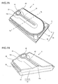
- FIG. 7A is a perspective view showing the structure of an LED chip 2 according to the second embodiment of the invention
- FIG. 7B is a perspective view including a cross-section taken along line 7b-7b of FIG. 7A
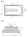
- FIG. 8A is a plan view
- FIG. 9 is a cross-sectional view taken along line 9-9 of FIG. 8 .
- An n-electrode 30 is formed on the surface of the n-layer 11 exposed by etching down part of the semiconductor film 14.
- the n-electrode has an n-pad 31 to be wire-bonded and a substantially U-shaped n-auxiliary electrode 32 connected to the n-pad 31.
- the p-layer 13 has a protruding portion 13a of trapezoidal cross-section in its extending surface that derives from the crystal structure of Al x In y Ga z N that is a hexagonal crystal. That is, the surfaces of the protruding portion 13a are constituted by crystal planes of Al x In y Ga z N.
- the protruding portion 13a extends along the center line of the LED chip 2 and the upper surface thereof is a flat surface.
- a p-electrode 40 is provided on the upper surface of the protruding portion 13a.
- the p-electrode 40 has a p-pad 41 to be wire-bonded and a p-auxiliary electrode 42 connected to the p-pad 41 and extending along the center line of the LED chip 2.
- the p-pad 41 and the p-auxiliary electrode 42 are both formed on the protruding portion 13a.
- the p-auxiliary electrode 42 together with the n-auxiliary electrode 32, has the role of relaxing or diminishing current concentration when the LED is driven, thus making the light emission brightness distribution uniform.
- the n-auxiliary electrode 32 and the p-auxiliary electrode 42 are placed such that the distance between both the electrodes is the same across the surface of the LED chip 2. By this means, the distribution of the light emission driving current flowing between both the electrodes becomes uniform across the surface of the LED chip 2, and thus the light emission brightness distribution can be made uniform.
- the surfaces of the p-electrode 40 and the p-layer 13 are covered by a light-transmissive electrode 20 made of, e.g., indium tin oxide (ITO).
- the light-transmissive electrode 20 is provided with an opening 21.
- the p-pad 41 is partially exposed through the opening 21, and can be wire-bonded.
- the p-pad 41 and the thin line-shaped p-auxiliary electrode 42 are formed directly on the semiconductor film 14 that is more likely to secure adhesion to them as compared with ITO or the like, and in addition are covered by the light-transmissive electrode 20 except the opening 21. Hence, they are unlikely to peel off even when thermal stress is applied thereto.
- the p-electrode 40 can be of multilayer structure as in the first embodiment. Further, the contact between the p-electrode 40 and the semiconductor film 14 is preferably non-ohmic contact (Schottky contact). By making the contact between the semiconductor film 14 and the p-electrode 40 be non-ohmic contact, current can be prevented from being concentrated directly under the p-electrode 40, and thus current can be diffused across the light-transmissive electrode 20.
- FIG. 10 is an enlarged cross-sectional view of the portion where the p-auxiliary electrode 42 is formed.
- the effective sheet resistance associated with the current path in the light-transmissive electrode 20 becomes lower as the thickness of the p-electrode 40 becomes greater, which provides an advantage in making current diffuse in the light-transmissive electrode 20.
- the thickness of the p-electrode 40 is too large, peeling-off due to thermal stress or the like is likely to occur.
- the effective sheet resistance of the light-transmissive electrode 20 can be reduced without an increase in the thickness of the p-electrode 40.
- the p-electrode 40 which includes the p-pad 40 and the p-auxiliary electrode 42 is provided on the upper surface of the protruding portion 13a of the p-layer 13 in the LED structure of the second embodiment. Therefore, the area of the cross-section through which current flowing out from the upper layer 403 of the p-electrode flows in the light-transmissive electrode 20 is greater than of the first embodiment. In other words, the current path (width "B" in FIG. 10 ) in a thickness direction of the light-transmissive electrode 20 is wider than in the first embodiment.
- the effective sheet resistance of the light-transmissive electrode 20 can be further reduced, enhancing current diffusion in the light-transmissive electrode 20 and contributing to the light emission brightness distribution being uniform across the surface. Further, with this structure, the current diffusion length in the light-transmissive electrode 20 can be extended, and hence the areas of the p-auxiliary electrode 42 and the n-auxiliary electrode 32 can be reduced. Thus, areas that are shadows in light emission can be reduced in size, hence further increasing the light output.
- the light extraction efficiency can be improved as compared with the case where the surface of the p-layer 13 is flat. This is because providing the p-layer 13 with the protruding portion 13a can reduce the amount of light which comes out of the light emitting layer 12 and reflected at the interface between the p-layer 13 and the light-transmissive electrode 20 by total reflection, thus not going outside.
- the protruding portion 13a can be formed in the growing step of the p-layer 13, and its shape derives from the crystal structure of Al x In y Ga z N that is a hexagonal crystal. Because the angle formed by the surface of the p-layer 13 and the inclined surface of the protruding portion 13a is constant and about 60 degrees, the width of the upper surface of the protruding portion 13a can be adjusted by its bottom width and height. By setting the height of the protruding portion 13a as large as or larger than the thickness of the light-transmissive electrode 20, the current path can be formed which utilizes the thickness of the light-transmissive electrode 20 to the maximum, enhancing current diffusion in the light-transmissive electrode 20.
- the thickness of the light-transmissive electrode 20 is preferably about 2,600 ⁇ , and the height of the protruding portion 13a is preferably greater than that.
- the height of the protruding portion 13a is preferably 5,000 ⁇ or greater. Note that the height of the protruding portion refers to the difference in level between the surface of the p-layer 13 around the protruding portion and the surface of the protruding portion 13a on which the p-electrode 40 is formed.
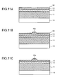
- the step for forming the protruding portion 13a (a protruding portion forming step) out of the production process of the LED chip 2 according to the second embodiment will be described with reference to FIGS. 11A to 11C .
- the semiconductor film forming step, the recess forming step, the electrode forming step, the light-transmissive electrode forming step, and the element separating step except the protruding portion forming step are the same as for the LED chip 1 according to the first embodiment, and hence description thereof is omitted.
- a SiO 2 film 50 is formed entirely over the surface of the p-layer 13.
- the SiO 2 film 50 is preferably formed by a thermal CVD method, an electron beam evaporation method, or the like, which does not expose the semiconductor film 14 to plasma.
- a resist mask (not shown) having an opening in its part corresponding to the forming area for the protruding portion 13a, is formed on the SiO 2 film 50, and part of the SiO 2 film 50 exposed through the opening of the resist mask is etched away using BHF (buffered hydrofluoric acid) to perform patterning of the SiO 2 film 50.
- BHF bufferevaporation
- the substrate is put into a MOCVD apparatus, and the semiconductor film is grown with the SiO 2 film 50 as a mask.
- a growth condition for forming the p-layer 13 that is, at an ambient temperature of 870°C, trimethylgallium (TMG) at a flow rate of 8.1 ⁇ mol/min, trimethylaluminum (TMA) at a flow rate of 7.5 ⁇ mol/min, ammonia (NH 3 ) at a flow rate of 4.4 LM, and CP2Mg (bis-cyclopentadienyl Mg) at a flow rate of 2.9 ⁇ 10 -7 ⁇ mol/min are supplied, thereby growing the p-GaN layer.
- TMG trimethylgallium
- TMA trimethylaluminum
- NH 3 ammonia
- CP2Mg bis-cyclopentadienyl Mg
- the p-GaN layer is grown on only part of the p-layer 13 exposed through the opening of the SiO 2 film 50 and forms the protruding portion 13a.
- the surfaces of the protruding portion 13a are constituted by crystal planes of Al X In y Ga z N, and the shape of a cross-section of the protruding portion 13a is a trapezoid.
- the height of the protruding portion 13a and the width of its upper surface can be adjusted by growth time ( FIG. 11B ).
- the substrate is immersed in BHF (buffered hydrofluoric acid) to remove the SiO 2 film 50 ( FIG. 11C ).
- BHF buffered hydrofluoric acid
- the protruding portion 13a is formed on the p-layer 13.
- the semiconductor film 14 is etched to make the n-layer 11 exposed; the n-electrode 30 and the p-electrode 40 are formed; the light-transmissive electrode 20 is formed to cover the p-electrode 40; the opening 21 is formed; and the resultant substrate is divided into LED chips.
- the LED chip 2 according to the second embodiment is fabricated.
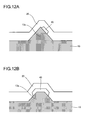
- the cross-section shape of the protruding portion 13a may be a triangle as shown in FIG. 12A , not being limited to a trapezoid.
- growth time for the p-GaN layer in the protruding portion forming step should be increased.
- the light output is expected to further increase by making the cross-section shape of the protruding portion 13a be a triangle.
- the p-electrode 40 may be formed on a side surface of the protruding portion 13a as shown in FIG. 12A , or formed straddling the top of the protruding portion 13a as shown in FIG. 12B .
- mask material for selective growth need only be a material that can stand crystal growth temperatures and can be patterned. For example, SiN or the like as well as SiO 2 can be used.
- LED chips having the p-layer as their upper surface have been described, but the p-layer and the n-layer may be inverted. That is, the present invention can be applied to the structure having the n-layer as the upper surface and the light-transmissive electrode placed on the n-layer.
Landscapes
- Led Devices (AREA)
Applications Claiming Priority (1)
| Application Number | Priority Date | Filing Date | Title |
|---|---|---|---|
| JP2009211537A JP5392611B2 (ja) | 2009-09-14 | 2009-09-14 | 半導体発光装置および半導体発光装置の製造方法 |
Publications (3)
| Publication Number | Publication Date |
|---|---|
| EP2296199A2 true EP2296199A2 (de) | 2011-03-16 |
| EP2296199A3 EP2296199A3 (de) | 2014-01-22 |
| EP2296199B1 EP2296199B1 (de) | 2019-04-24 |
Family
ID=43242006
Family Applications (1)
| Application Number | Title | Priority Date | Filing Date |
|---|---|---|---|
| EP10009249.3A Not-in-force EP2296199B1 (de) | 2009-09-14 | 2010-09-06 | Lichtemittierende Halbleitervorrichtung und Herstellungsverfahren davon |
Country Status (4)
| Country | Link |
|---|---|
| US (1) | US8455912B2 (de) |
| EP (1) | EP2296199B1 (de) |
| JP (1) | JP5392611B2 (de) |
| KR (1) | KR101708939B1 (de) |
Cited By (1)
| Publication number | Priority date | Publication date | Assignee | Title |
|---|---|---|---|---|
| EP2565941A3 (de) * | 2011-08-30 | 2014-11-19 | LG Innotek Co., Ltd. | Lichtemittierende Vorrichtung |
Families Citing this family (25)
| Publication number | Priority date | Publication date | Assignee | Title |
|---|---|---|---|---|
| JP5494005B2 (ja) | 2010-02-26 | 2014-05-14 | 豊田合成株式会社 | 半導体発光素子 |
| US8536595B2 (en) * | 2010-08-31 | 2013-09-17 | Micron Technology, Inc. | Solid state lighting devices with low contact resistance and methods of manufacturing |
| JP5960426B2 (ja) * | 2011-12-16 | 2016-08-02 | スタンレー電気株式会社 | 半導体素子及び半導体素子の製造方法 |
| KR101883842B1 (ko) * | 2011-12-26 | 2018-08-01 | 엘지이노텍 주식회사 | 발광소자 및 이를 포함하는 조명시스템 |
| TWD154431S (zh) * | 2012-10-03 | 2013-07-01 | 晶元光電股份有限公司 | 發光二極體 |
| JP5435523B1 (ja) * | 2012-10-12 | 2014-03-05 | エルシード株式会社 | 半導体発光素子及びその製造方法 |
| JP6102677B2 (ja) * | 2012-12-28 | 2017-03-29 | 日亜化学工業株式会社 | 発光素子 |
| TWI514628B (zh) | 2013-10-24 | 2015-12-21 | Lextar Electronics Corp | 電極結構與具有電極結構的發光二極體結構 |
| WO2015074353A1 (zh) * | 2013-11-25 | 2015-05-28 | 扬州中科半导体照明有限公司 | 一种半导体发光二极管芯片 |
| JP6443198B2 (ja) * | 2014-04-25 | 2018-12-26 | 日亜化学工業株式会社 | 発光素子 |
| USD773410S1 (en) * | 2014-10-24 | 2016-12-06 | Epistar Corporation | Light-emitting diode array |
| JP2016127064A (ja) * | 2014-12-26 | 2016-07-11 | 株式会社東芝 | 半導体発光素子及びその製造方法 |
| TWI583019B (zh) * | 2015-02-17 | 2017-05-11 | 新世紀光電股份有限公司 | Light emitting diode and manufacturing method thereof |
| USD770989S1 (en) * | 2015-02-23 | 2016-11-08 | Seoul Viosys Co., Ltd. | Light emitting diode |
| CN110323310B (zh) * | 2015-04-22 | 2021-04-13 | 新世纪光电股份有限公司 | 发光二极管 |
| USD775090S1 (en) * | 2015-04-23 | 2016-12-27 | Seoul Viosys Co., Ltd. | Light emitting diode |
| DE102016106571A1 (de) * | 2016-04-11 | 2017-10-12 | Osram Opto Semiconductors Gmbh | Lichtemittierender Halbleiterchip, lichtemittierendes Bauelement und Verfahren zur Herstellung eines lichtemittierenden Bauelements |
| CN105845801B (zh) * | 2016-06-13 | 2018-04-10 | 天津三安光电有限公司 | 发光二极管及其制作方法 |
| TWD190563S (zh) * | 2017-06-23 | 2018-05-21 | 晶元光電股份有限公司 | 發光二極體陣列之部分 |
| CN111725375A (zh) | 2019-03-22 | 2020-09-29 | 新世纪光电股份有限公司 | 红光发光二极管及其制造方法 |
| JP7245101B2 (ja) * | 2019-04-02 | 2023-03-23 | キヤノン株式会社 | 半導体発光装置、露光ヘッド及び画像形成装置 |
| US20220352418A1 (en) * | 2019-11-12 | 2022-11-03 | Sony Group Corporation | Semiconductor light emitting element and electronic apparatus |
| JP7216295B2 (ja) * | 2020-09-28 | 2023-02-01 | 日亜化学工業株式会社 | 発光素子 |
| CN113437188A (zh) * | 2021-06-24 | 2021-09-24 | 厦门乾照光电股份有限公司 | 一种led芯片及其制备方法 |
| CN116936708A (zh) * | 2023-08-14 | 2023-10-24 | 厦门乾照光电股份有限公司 | 一种led芯片及其制作方法 |
Citations (1)
| Publication number | Priority date | Publication date | Assignee | Title |
|---|---|---|---|---|
| JP2001345480A (ja) | 2000-03-31 | 2001-12-14 | Toyoda Gosei Co Ltd | Iii族窒化物系化合物半導体素子 |
Family Cites Families (9)
| Publication number | Priority date | Publication date | Assignee | Title |
|---|---|---|---|---|
| WO1994015369A1 (en) * | 1992-12-22 | 1994-07-07 | Research Corporation Technologies, Inc. | Group ii-vi compound semiconductor light emitting devices and an ohmic contact therefor |
| JP3916011B2 (ja) * | 1997-02-21 | 2007-05-16 | シャープ株式会社 | 窒化ガリウム系化合物半導体発光素子及びその製造方法 |
| JPH1187772A (ja) * | 1997-09-01 | 1999-03-30 | Showa Denko Kk | 半導体発光素子用の電極 |
| JPH11135834A (ja) * | 1997-10-27 | 1999-05-21 | Matsushita Electric Ind Co Ltd | 発光ダイオード装置及びその製造方法 |
| JP2005116794A (ja) * | 2003-10-08 | 2005-04-28 | Mitsubishi Cable Ind Ltd | 窒化物半導体発光素子 |
| JP2006156590A (ja) * | 2004-11-26 | 2006-06-15 | Mitsubishi Cable Ind Ltd | 発光ダイオード |
| CN102779918B (zh) * | 2007-02-01 | 2015-09-02 | 日亚化学工业株式会社 | 半导体发光元件 |
| US8115222B2 (en) * | 2008-01-16 | 2012-02-14 | Rohm Co., Ltd. | Semiconductor light emitting device and fabrication method for the semiconductor light emitting device |
| WO2010113238A1 (ja) * | 2009-04-03 | 2010-10-07 | パナソニック株式会社 | 窒化物系半導体素子およびその製造方法 |
-
2009
- 2009-09-14 JP JP2009211537A patent/JP5392611B2/ja not_active Expired - Fee Related
-
2010
- 2010-09-06 EP EP10009249.3A patent/EP2296199B1/de not_active Not-in-force
- 2010-09-08 KR KR1020100088010A patent/KR101708939B1/ko active Active
- 2010-09-09 US US12/878,197 patent/US8455912B2/en not_active Expired - Fee Related
Patent Citations (1)
| Publication number | Priority date | Publication date | Assignee | Title |
|---|---|---|---|---|
| JP2001345480A (ja) | 2000-03-31 | 2001-12-14 | Toyoda Gosei Co Ltd | Iii族窒化物系化合物半導体素子 |
Cited By (2)
| Publication number | Priority date | Publication date | Assignee | Title |
|---|---|---|---|---|
| EP2565941A3 (de) * | 2011-08-30 | 2014-11-19 | LG Innotek Co., Ltd. | Lichtemittierende Vorrichtung |
| US9130117B2 (en) | 2011-08-30 | 2015-09-08 | Lg Innotek Co., Ltd. | Light emitting device |
Also Published As
| Publication number | Publication date |
|---|---|
| US20110062484A1 (en) | 2011-03-17 |
| JP2011061127A (ja) | 2011-03-24 |
| KR20110029085A (ko) | 2011-03-22 |
| US8455912B2 (en) | 2013-06-04 |
| EP2296199B1 (de) | 2019-04-24 |
| EP2296199A3 (de) | 2014-01-22 |
| KR101708939B1 (ko) | 2017-03-08 |
| JP5392611B2 (ja) | 2014-01-22 |
Similar Documents
| Publication | Publication Date | Title |
|---|---|---|
| US8455912B2 (en) | Semiconductor light emitting device and manufacturing method thereof | |
| JP5343860B2 (ja) | GaN系LED素子用電極およびGaN系LED素子ならびにそれらの製造方法。 | |
| US8158994B2 (en) | GaN LED element and light emitting device having a structure to reduce light absorption by a pad electrode included therein | |
| TWI445205B (zh) | Semiconductor light emitting element | |
| EP2595202B1 (de) | Lichtemittierendes Halbleiterelement und Herstellungsverfahren für ein lichtemittierendes Halbleiterelement | |
| US9099627B2 (en) | Method for producing group III nitride semiconductor light-emitting device | |
| WO2005050748A1 (ja) | 半導体素子及びその製造方法 | |
| JP2006128227A (ja) | 窒化物半導体発光素子 | |
| JP2008227109A (ja) | GaN系LED素子および発光装置 | |
| WO2008047923A1 (en) | Nitride semiconductor light-emitting diode device | |
| TWI334650B (en) | Gallium nitride-based compound semiconductor light-emitting device | |
| JP2008218878A (ja) | GaN系LED素子および発光装置 | |
| JP5845557B2 (ja) | 半導体発光素子の製造方法 | |
| JP4803302B2 (ja) | 窒化物半導体発光素子 | |
| US6420731B1 (en) | Light emitting diode and manufacturing method thereof | |
| JP4835376B2 (ja) | 半導体発光素子 | |
| CN115548187A (zh) | 发光二极管和发光装置 | |
| JP5630276B2 (ja) | 半導体発光素子、半導体発光装置 | |
| KR101337617B1 (ko) | 오믹 전극 패턴을 갖는 수직형 발광 다이오드 및 그제조방법 | |
| CN112670382B (zh) | 一种led芯片及led芯片的制备方法 | |
| CN108365056A (zh) | 一种垂直结构发光二极管及其制造方法 | |
| JP4751093B2 (ja) | 半導体発光素子 | |
| KR20110080455A (ko) | 발광소자 및 이의 제조방법 |
Legal Events
| Date | Code | Title | Description |
|---|---|---|---|
| PUAI | Public reference made under article 153(3) epc to a published international application that has entered the european phase |
Free format text: ORIGINAL CODE: 0009012 |
|
| AK | Designated contracting states |
Kind code of ref document: A2 Designated state(s): AL AT BE BG CH CY CZ DE DK EE ES FI FR GB GR HR HU IE IS IT LI LT LU LV MC MK MT NL NO PL PT RO SE SI SK SM TR |
|
| AX | Request for extension of the european patent |
Extension state: BA ME RS |
|
| PUAL | Search report despatched |
Free format text: ORIGINAL CODE: 0009013 |
|
| AK | Designated contracting states |
Kind code of ref document: A3 Designated state(s): AL AT BE BG CH CY CZ DE DK EE ES FI FR GB GR HR HU IE IS IT LI LT LU LV MC MK MT NL NO PL PT RO SE SI SK SM TR |
|
| AX | Request for extension of the european patent |
Extension state: BA ME RS |
|
| RIC1 | Information provided on ipc code assigned before grant |
Ipc: H01L 33/38 20100101AFI20131219BHEP Ipc: H01L 33/20 20100101ALI20131219BHEP |
|
| 17P | Request for examination filed |
Effective date: 20140722 |
|
| RBV | Designated contracting states (corrected) |
Designated state(s): AL AT BE BG CH CY CZ DE DK EE ES FI FR GB GR HR HU IE IS IT LI LT LU LV MC MK MT NL NO PL PT RO SE SI SK SM TR |
|
| STAA | Information on the status of an ep patent application or granted ep patent |
Free format text: STATUS: EXAMINATION IS IN PROGRESS |
|
| 17Q | First examination report despatched |
Effective date: 20170118 |
|
| GRAP | Despatch of communication of intention to grant a patent |
Free format text: ORIGINAL CODE: EPIDOSNIGR1 |
|
| STAA | Information on the status of an ep patent application or granted ep patent |
Free format text: STATUS: GRANT OF PATENT IS INTENDED |
|
| INTG | Intention to grant announced |
Effective date: 20181120 |
|
| GRAS | Grant fee paid |
Free format text: ORIGINAL CODE: EPIDOSNIGR3 |
|
| GRAA | (expected) grant |
Free format text: ORIGINAL CODE: 0009210 |
|
| STAA | Information on the status of an ep patent application or granted ep patent |
Free format text: STATUS: THE PATENT HAS BEEN GRANTED |
|
| AK | Designated contracting states |
Kind code of ref document: B1 Designated state(s): AL AT BE BG CH CY CZ DE DK EE ES FI FR GB GR HR HU IE IS IT LI LT LU LV MC MK MT NL NO PL PT RO SE SI SK SM TR |
|
| REG | Reference to a national code |
Ref country code: GB Ref legal event code: FG4D |
|
| REG | Reference to a national code |
Ref country code: CH Ref legal event code: EP |
|
| REG | Reference to a national code |
Ref country code: AT Ref legal event code: REF Ref document number: 1125174 Country of ref document: AT Kind code of ref document: T Effective date: 20190515 Ref country code: IE Ref legal event code: FG4D |
|
| REG | Reference to a national code |
Ref country code: DE Ref legal event code: R096 Ref document number: 602010058380 Country of ref document: DE |
|
| REG | Reference to a national code |
Ref country code: NL Ref legal event code: MP Effective date: 20190424 |
|
| REG | Reference to a national code |
Ref country code: LT Ref legal event code: MG4D |
|
| PG25 | Lapsed in a contracting state [announced via postgrant information from national office to epo] |
Ref country code: NL Free format text: LAPSE BECAUSE OF FAILURE TO SUBMIT A TRANSLATION OF THE DESCRIPTION OR TO PAY THE FEE WITHIN THE PRESCRIBED TIME-LIMIT Effective date: 20190424 |
|
| PG25 | Lapsed in a contracting state [announced via postgrant information from national office to epo] |
Ref country code: FI Free format text: LAPSE BECAUSE OF FAILURE TO SUBMIT A TRANSLATION OF THE DESCRIPTION OR TO PAY THE FEE WITHIN THE PRESCRIBED TIME-LIMIT Effective date: 20190424 Ref country code: LT Free format text: LAPSE BECAUSE OF FAILURE TO SUBMIT A TRANSLATION OF THE DESCRIPTION OR TO PAY THE FEE WITHIN THE PRESCRIBED TIME-LIMIT Effective date: 20190424 Ref country code: AL Free format text: LAPSE BECAUSE OF FAILURE TO SUBMIT A TRANSLATION OF THE DESCRIPTION OR TO PAY THE FEE WITHIN THE PRESCRIBED TIME-LIMIT Effective date: 20190424 Ref country code: ES Free format text: LAPSE BECAUSE OF FAILURE TO SUBMIT A TRANSLATION OF THE DESCRIPTION OR TO PAY THE FEE WITHIN THE PRESCRIBED TIME-LIMIT Effective date: 20190424 Ref country code: SE Free format text: LAPSE BECAUSE OF FAILURE TO SUBMIT A TRANSLATION OF THE DESCRIPTION OR TO PAY THE FEE WITHIN THE PRESCRIBED TIME-LIMIT Effective date: 20190424 Ref country code: NO Free format text: LAPSE BECAUSE OF FAILURE TO SUBMIT A TRANSLATION OF THE DESCRIPTION OR TO PAY THE FEE WITHIN THE PRESCRIBED TIME-LIMIT Effective date: 20190724 Ref country code: PT Free format text: LAPSE BECAUSE OF FAILURE TO SUBMIT A TRANSLATION OF THE DESCRIPTION OR TO PAY THE FEE WITHIN THE PRESCRIBED TIME-LIMIT Effective date: 20190824 Ref country code: HR Free format text: LAPSE BECAUSE OF FAILURE TO SUBMIT A TRANSLATION OF THE DESCRIPTION OR TO PAY THE FEE WITHIN THE PRESCRIBED TIME-LIMIT Effective date: 20190424 |
|
| PG25 | Lapsed in a contracting state [announced via postgrant information from national office to epo] |
Ref country code: GR Free format text: LAPSE BECAUSE OF FAILURE TO SUBMIT A TRANSLATION OF THE DESCRIPTION OR TO PAY THE FEE WITHIN THE PRESCRIBED TIME-LIMIT Effective date: 20190725 Ref country code: PL Free format text: LAPSE BECAUSE OF FAILURE TO SUBMIT A TRANSLATION OF THE DESCRIPTION OR TO PAY THE FEE WITHIN THE PRESCRIBED TIME-LIMIT Effective date: 20190424 Ref country code: LV Free format text: LAPSE BECAUSE OF FAILURE TO SUBMIT A TRANSLATION OF THE DESCRIPTION OR TO PAY THE FEE WITHIN THE PRESCRIBED TIME-LIMIT Effective date: 20190424 Ref country code: BG Free format text: LAPSE BECAUSE OF FAILURE TO SUBMIT A TRANSLATION OF THE DESCRIPTION OR TO PAY THE FEE WITHIN THE PRESCRIBED TIME-LIMIT Effective date: 20190724 |
|
| REG | Reference to a national code |
Ref country code: AT Ref legal event code: MK05 Ref document number: 1125174 Country of ref document: AT Kind code of ref document: T Effective date: 20190424 |
|
| PG25 | Lapsed in a contracting state [announced via postgrant information from national office to epo] |
Ref country code: IS Free format text: LAPSE BECAUSE OF FAILURE TO SUBMIT A TRANSLATION OF THE DESCRIPTION OR TO PAY THE FEE WITHIN THE PRESCRIBED TIME-LIMIT Effective date: 20190824 |
|
| REG | Reference to a national code |
Ref country code: DE Ref legal event code: R097 Ref document number: 602010058380 Country of ref document: DE |
|
| PG25 | Lapsed in a contracting state [announced via postgrant information from national office to epo] |
Ref country code: EE Free format text: LAPSE BECAUSE OF FAILURE TO SUBMIT A TRANSLATION OF THE DESCRIPTION OR TO PAY THE FEE WITHIN THE PRESCRIBED TIME-LIMIT Effective date: 20190424 Ref country code: AT Free format text: LAPSE BECAUSE OF FAILURE TO SUBMIT A TRANSLATION OF THE DESCRIPTION OR TO PAY THE FEE WITHIN THE PRESCRIBED TIME-LIMIT Effective date: 20190424 Ref country code: RO Free format text: LAPSE BECAUSE OF FAILURE TO SUBMIT A TRANSLATION OF THE DESCRIPTION OR TO PAY THE FEE WITHIN THE PRESCRIBED TIME-LIMIT Effective date: 20190424 Ref country code: CZ Free format text: LAPSE BECAUSE OF FAILURE TO SUBMIT A TRANSLATION OF THE DESCRIPTION OR TO PAY THE FEE WITHIN THE PRESCRIBED TIME-LIMIT Effective date: 20190424 Ref country code: SK Free format text: LAPSE BECAUSE OF FAILURE TO SUBMIT A TRANSLATION OF THE DESCRIPTION OR TO PAY THE FEE WITHIN THE PRESCRIBED TIME-LIMIT Effective date: 20190424 Ref country code: DK Free format text: LAPSE BECAUSE OF FAILURE TO SUBMIT A TRANSLATION OF THE DESCRIPTION OR TO PAY THE FEE WITHIN THE PRESCRIBED TIME-LIMIT Effective date: 20190424 |
|
| PG25 | Lapsed in a contracting state [announced via postgrant information from national office to epo] |
Ref country code: SM Free format text: LAPSE BECAUSE OF FAILURE TO SUBMIT A TRANSLATION OF THE DESCRIPTION OR TO PAY THE FEE WITHIN THE PRESCRIBED TIME-LIMIT Effective date: 20190424 Ref country code: IT Free format text: LAPSE BECAUSE OF FAILURE TO SUBMIT A TRANSLATION OF THE DESCRIPTION OR TO PAY THE FEE WITHIN THE PRESCRIBED TIME-LIMIT Effective date: 20190424 |
|
| PLBE | No opposition filed within time limit |
Free format text: ORIGINAL CODE: 0009261 |
|
| STAA | Information on the status of an ep patent application or granted ep patent |
Free format text: STATUS: NO OPPOSITION FILED WITHIN TIME LIMIT |
|
| PG25 | Lapsed in a contracting state [announced via postgrant information from national office to epo] |
Ref country code: TR Free format text: LAPSE BECAUSE OF FAILURE TO SUBMIT A TRANSLATION OF THE DESCRIPTION OR TO PAY THE FEE WITHIN THE PRESCRIBED TIME-LIMIT Effective date: 20190424 |
|
| 26N | No opposition filed |
Effective date: 20200127 |
|
| PG25 | Lapsed in a contracting state [announced via postgrant information from national office to epo] |
Ref country code: MC Free format text: LAPSE BECAUSE OF FAILURE TO SUBMIT A TRANSLATION OF THE DESCRIPTION OR TO PAY THE FEE WITHIN THE PRESCRIBED TIME-LIMIT Effective date: 20190424 Ref country code: SI Free format text: LAPSE BECAUSE OF FAILURE TO SUBMIT A TRANSLATION OF THE DESCRIPTION OR TO PAY THE FEE WITHIN THE PRESCRIBED TIME-LIMIT Effective date: 20190424 |
|
| REG | Reference to a national code |
Ref country code: CH Ref legal event code: PL |
|
| PG25 | Lapsed in a contracting state [announced via postgrant information from national office to epo] |
Ref country code: LI Free format text: LAPSE BECAUSE OF NON-PAYMENT OF DUE FEES Effective date: 20190930 Ref country code: LU Free format text: LAPSE BECAUSE OF NON-PAYMENT OF DUE FEES Effective date: 20190906 Ref country code: IE Free format text: LAPSE BECAUSE OF NON-PAYMENT OF DUE FEES Effective date: 20190906 Ref country code: CH Free format text: LAPSE BECAUSE OF NON-PAYMENT OF DUE FEES Effective date: 20190930 |
|
| REG | Reference to a national code |
Ref country code: BE Ref legal event code: MM Effective date: 20190930 |
|
| PG25 | Lapsed in a contracting state [announced via postgrant information from national office to epo] |
Ref country code: BE Free format text: LAPSE BECAUSE OF NON-PAYMENT OF DUE FEES Effective date: 20190930 |
|
| PG25 | Lapsed in a contracting state [announced via postgrant information from national office to epo] |
Ref country code: CY Free format text: LAPSE BECAUSE OF FAILURE TO SUBMIT A TRANSLATION OF THE DESCRIPTION OR TO PAY THE FEE WITHIN THE PRESCRIBED TIME-LIMIT Effective date: 20190424 |
|
| PG25 | Lapsed in a contracting state [announced via postgrant information from national office to epo] |
Ref country code: HU Free format text: LAPSE BECAUSE OF FAILURE TO SUBMIT A TRANSLATION OF THE DESCRIPTION OR TO PAY THE FEE WITHIN THE PRESCRIBED TIME-LIMIT; INVALID AB INITIO Effective date: 20100906 Ref country code: MT Free format text: LAPSE BECAUSE OF FAILURE TO SUBMIT A TRANSLATION OF THE DESCRIPTION OR TO PAY THE FEE WITHIN THE PRESCRIBED TIME-LIMIT Effective date: 20190424 |
|
| PG25 | Lapsed in a contracting state [announced via postgrant information from national office to epo] |
Ref country code: MK Free format text: LAPSE BECAUSE OF FAILURE TO SUBMIT A TRANSLATION OF THE DESCRIPTION OR TO PAY THE FEE WITHIN THE PRESCRIBED TIME-LIMIT Effective date: 20190424 |
|
| PGFP | Annual fee paid to national office [announced via postgrant information from national office to epo] |
Ref country code: GB Payment date: 20230727 Year of fee payment: 14 |
|
| PGFP | Annual fee paid to national office [announced via postgrant information from national office to epo] |
Ref country code: FR Payment date: 20230808 Year of fee payment: 14 Ref country code: DE Payment date: 20230802 Year of fee payment: 14 |
|
| REG | Reference to a national code |
Ref country code: DE Ref legal event code: R079 Ref document number: 602010058380 Country of ref document: DE Free format text: PREVIOUS MAIN CLASS: H01L0033380000 Ipc: H10H0020831000 |
|
| REG | Reference to a national code |
Ref country code: DE Ref legal event code: R119 Ref document number: 602010058380 Country of ref document: DE |
|
| GBPC | Gb: european patent ceased through non-payment of renewal fee |
Effective date: 20240906 |
|
| PG25 | Lapsed in a contracting state [announced via postgrant information from national office to epo] |
Ref country code: DE Free format text: LAPSE BECAUSE OF NON-PAYMENT OF DUE FEES Effective date: 20250401 |
|
| PG25 | Lapsed in a contracting state [announced via postgrant information from national office to epo] |
Ref country code: GB Free format text: LAPSE BECAUSE OF NON-PAYMENT OF DUE FEES Effective date: 20240906 |
|
| PG25 | Lapsed in a contracting state [announced via postgrant information from national office to epo] |
Ref country code: FR Free format text: LAPSE BECAUSE OF NON-PAYMENT OF DUE FEES Effective date: 20240930 |