EP2296248A2 - Procédé et système pour distinguer des ports de chargement - Google Patents
Procédé et système pour distinguer des ports de chargement Download PDFInfo
- Publication number
- EP2296248A2 EP2296248A2 EP10008957A EP10008957A EP2296248A2 EP 2296248 A2 EP2296248 A2 EP 2296248A2 EP 10008957 A EP10008957 A EP 10008957A EP 10008957 A EP10008957 A EP 10008957A EP 2296248 A2 EP2296248 A2 EP 2296248A2
- Authority
- EP
- European Patent Office
- Prior art keywords
- switch
- data line
- charging port
- cdp
- voltage
- Prior art date
- Legal status (The legal status is an assumption and is not a legal conclusion. Google has not performed a legal analysis and makes no representation as to the accuracy of the status listed.)
- Granted
Links
Images




Classifications
-
- H—ELECTRICITY
- H02—GENERATION; CONVERSION OR DISTRIBUTION OF ELECTRIC POWER
- H02J—ELECTRIC POWER NETWORKS; CIRCUIT ARRANGEMENTS OR SYSTEMS FOR SUPPLYING OR DISTRIBUTING ELECTRIC POWER; SYSTEMS FOR STORING ELECTRIC ENERGY
- H02J7/00—Circuit arrangements for charging or discharging batteries or for supplying loads from batteries
- H02J7/485—Circuit arrangements for charging or discharging batteries or for supplying loads from batteries with provisions for charging different types of batteries
-
- H—ELECTRICITY
- H02—GENERATION; CONVERSION OR DISTRIBUTION OF ELECTRIC POWER
- H02J—ELECTRIC POWER NETWORKS; CIRCUIT ARRANGEMENTS OR SYSTEMS FOR SUPPLYING OR DISTRIBUTING ELECTRIC POWER; SYSTEMS FOR STORING ELECTRIC ENERGY
- H02J7/00—Circuit arrangements for charging or discharging batteries or for supplying loads from batteries
-
- H—ELECTRICITY
- H02—GENERATION; CONVERSION OR DISTRIBUTION OF ELECTRIC POWER
- H02J—ELECTRIC POWER NETWORKS; CIRCUIT ARRANGEMENTS OR SYSTEMS FOR SUPPLYING OR DISTRIBUTING ELECTRIC POWER; SYSTEMS FOR STORING ELECTRIC ENERGY
- H02J7/00—Circuit arrangements for charging or discharging batteries or for supplying loads from batteries
- H02J7/40—Circuit arrangements for charging or discharging batteries or for supplying loads from batteries characterised by the exchange of charge or discharge related data
- H02J7/44—Circuit arrangements for charging or discharging batteries or for supplying loads from batteries characterised by the exchange of charge or discharge related data between battery management systems and power sources
-
- H—ELECTRICITY
- H02—GENERATION; CONVERSION OR DISTRIBUTION OF ELECTRIC POWER
- H02J—ELECTRIC POWER NETWORKS; CIRCUIT ARRANGEMENTS OR SYSTEMS FOR SUPPLYING OR DISTRIBUTING ELECTRIC POWER; SYSTEMS FOR STORING ELECTRIC ENERGY
- H02J7/00—Circuit arrangements for charging or discharging batteries or for supplying loads from batteries
- H02J7/40—Circuit arrangements for charging or discharging batteries or for supplying loads from batteries characterised by the exchange of charge or discharge related data
- H02J7/443—Circuit arrangements for charging or discharging batteries or for supplying loads from batteries characterised by the exchange of charge or discharge related data using passive battery identification means, e.g. resistors or capacitors
-
- H—ELECTRICITY
- H02—GENERATION; CONVERSION OR DISTRIBUTION OF ELECTRIC POWER
- H02J—ELECTRIC POWER NETWORKS; CIRCUIT ARRANGEMENTS OR SYSTEMS FOR SUPPLYING OR DISTRIBUTING ELECTRIC POWER; SYSTEMS FOR STORING ELECTRIC ENERGY
- H02J7/00—Circuit arrangements for charging or discharging batteries or for supplying loads from batteries
- H02J7/40—Circuit arrangements for charging or discharging batteries or for supplying loads from batteries characterised by the exchange of charge or discharge related data
- H02J7/47—Arrangements for checking compatibility or authentication between one component, e.g. a battery or a battery charger, and another component, e.g. a power source
-
- Y—GENERAL TAGGING OF NEW TECHNOLOGICAL DEVELOPMENTS; GENERAL TAGGING OF CROSS-SECTIONAL TECHNOLOGIES SPANNING OVER SEVERAL SECTIONS OF THE IPC; TECHNICAL SUBJECTS COVERED BY FORMER USPC CROSS-REFERENCE ART COLLECTIONS [XRACs] AND DIGESTS
- Y02—TECHNOLOGIES OR APPLICATIONS FOR MITIGATION OR ADAPTATION AGAINST CLIMATE CHANGE
- Y02E—REDUCTION OF GREENHOUSE GAS [GHG] EMISSIONS, RELATED TO ENERGY GENERATION, TRANSMISSION OR DISTRIBUTION
- Y02E60/00—Enabling technologies; Technologies with a potential or indirect contribution to GHG emissions mitigation
- Y02E60/10—Energy storage using batteries
Definitions
- the present invention is generally in the field of communication methods and systems. More specifically, the present invention is in the field of network communication methods and systems.
- USB ports provide convenient locations and an efficient power solution to charge portable devices using a widely adaptable USB cable and a personal computer, hub or USB charger.
- Portable devices must accommodate the fact that a personal computer or hub draws a different amount of current than a USB charger. Consequently, a portable device must distinguish between different types of charging ports, including a Dedicated Charging Port (“DCP”) - a charging port corresponding to a USB charger, and a Charging Downstream Port (“CDP”) - a charging port corresponding to a personal computer or hub.
- DCP Dedicated Charging Port
- CDP Charging Downstream Port
- FIG. 1 shows dedicated charging port ("DCP") circuit 100 adapted to connect to a portable device.
- Supply voltage pin 106 provides a positive supply voltage of a value V BUS to DCP circuit 100
- ground pin 112 provides a ground voltage to DCP circuit 100.
- Positive data line 108 and negative data line 110 are connected through a resistor or resistive network such as resistor 104 with value R CHG_DAT .
- V BUS operates at 5.25 Volts (V) and R CHG_DAT has a value of 200 ohms.
- DCP circuit 100 may provide a portable device with up to 1.8 Amperes (A) of current at 5.25 V through supply voltage pin 106.
- DCP circuit 100 shorts positive data line 108 and negative data line 110 with resistor 104, DCP circuit 100 does not transfer data to or from a connected portable device. For example, a binary signal that has a step transition between a logical LOW value of below 0.8 V and a logical HIGH value of above 2.0 V on positive data line 108 merely returns to negative data line 110 through resistor. Consequently, DCP circuit 100 can charge a portable device but is incapable of processing logical data for a portable device or supporting data communications between a host and a device.
- FIG. 2 illustrates charging downstream port (“CDP") circuit 200.
- CDP circuit 200 includes supply voltage pin 206, ground pin 212, positive data line 208 and negative data line 210. These pins are similar to respective pins illustrated in DCP circuit 100 of FIG. 1 .
- CDP circuit 200 includes positive switch 236, positive pull-down resistor 220, comparator 228, positive data line current sink 230, negative data line voltage source 224, negative switch 226, negative pull-down resistor 222, and AND gate 240.
- Portable detect signal 238 comes from AND gate 240 into physical layer 204.
- Portable detect signal 238 may be configured to correspond to digital logic values, including for example, a value of 0 to 0.8 V corresponding to a logical LOW signal and a value of above 2.0 V corresponding to a logical HIGH signal.
- CDP circuit 200 includes comparator 228, as well as leakage resistors 216 and leakage voltages 218.
- Positive data line current sink 230 is configured to draw between 50 and 150 microamperes ( ⁇ A) of current.
- Negative data line voltage source 224 is configured to provide between 0.5 and 0.7 V.
- Data detect voltage 232 provides a voltage between 0.25 and 0.4 V.
- CDP circuit 200 in FIG. 2 is capable of supporting data communication between a host coupled thereto and a device. More specifically, CDP circuit 200 can receive differential signals corresponding to logical LOW or logical HIGH voltages in differential form across positive data line 208 and negative data line 210. These differential voltages may correspond to packetized information, including for example, control instructions or data, which are used for communicate between the portable device and a host coupled to CDP circuit 200.
- One means of communication via a CDP circuit 200 is by driving a voltage equal to negative data line voltage source 224 onto negative data line 210.
- CDP circuit 200 receives a voltage on positive data line 208 that is greater than data detect voltage 232 and is less than the logic threshold of CDP circuit 200 (namely below the logical LOW threshold voltage value of 0.8 V), portable detect signal 238 is asserted.
- CDP circuit 200 actively responds to this signal by switching negative switch 226 and driving the voltage at negative data line voltage source 224 onto negative data line 210, actively transmitting that value back to the portable device.
- a voltage on positive data line 210 lies between 0.4 V (the maximum value of data detect voltage source 224) and 0.8 V (the minimum value of the logic threshold voltage)
- a voltage of between 0.5 V and 0.7 V corresponding to negative data line voltage source 224 will be applied to negative data line 210 and transmitted back to the portable device.
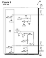
- FIG. 3 illustrates conventional portable device circuit 300 adapted to connect to either a DCP or a CDP.
- Conventional portable device circuit 300 comprises pins to interface to a DCP or a CDP, including supply voltage pin 306 to draw charge, ground pin 312, positive data line 308, negative data line 310 and ID pin 314. Positive data line 308 and negative data line 310 allow conventional portable device circuit 300 to distinguish between a DCP or a CDP using logical signals in differential form.
- conventional portable device circuit 300 includes voltage switch 352, current switch 354, comparator switch 356, pull-down switch 368, and pull down resistor 370.
- Conventional portable device circuit 300 further includes positive data line voltage source 348, data connect detect current source 350, negative data line current sink 358, data detect voltage 360 and AND gate 364.
- Comparator 362 is capable of comparing data detect voltage 360 with a voltage on negative data line 310.
- Charger detect signal 366 comes into physical layer 342 through AND gate 364.
- Physical layer 342 includes leakage resistors 344 with leakage voltages 346.
- Negative data line current sink 358 is configured to draw between 50 and 150 microamperes ( ⁇ A) of current.
- Positive data line voltage source 348 is configured to provide between 0.5 and 0.7 V.
- conventional portable device circuit 300 is required to detect a charging port and classify the detected charging port as a DCP or a CDP to determine how much current it can draw from the charging port.
- Conventional portable device circuit 300 begins operation in low bandwidth of full bandwidth mode.
- Conventional portable device circuit 300 then closes voltage switch 352, current switch 354 and comparator switch 356 to raise the voltage on positive data line 308 to positive data line source voltage 348, that is to a logical HIGH.
- conventional portable device circuit 300 After a positive voltage source on time of about 40 milliseconds (ms), conventional portable device circuit 300 then checks the voltage at negative data line 310. If the voltage at negative data line 310 is above data detect voltage 360 but below the logic threshold of conventional portable device circuit 300, conventional portable device circuit 300 has detected that a charging port is attached and is allowed to draw a specified portable device current from the charging port.
- conventional portable device circuit 300 To classify the attached charging port as a DCP or a CDP, conventional portable device circuit 300 asserts a logical HIGH value (that is a value exceeding the circuit's logical threshold voltage of 2.0 V) onto positive data line 308. If the attached charging port is a DCP, the voltage on negative data line 310 will also go to a logical HIGH value, because a DCP shorts positive data line 308 and negative data line 310 through an internal resistor (shown in FIG. 1 ). Thus, despite the presence of the internal resistor, the voltage at negative data line will reach a logical HIGH value and allow conventional portable device circuit 300 to determine that a DCP is connected. In such a case, conventional portable device circuit 300 and may attempt to draw a current of up to 1.8 A.
- the voltage on positive data line 308 will cause a communication with the portable device. Consistent with FIG. 3 , the voltage on positive data line 308 will correspond to a logical HIGH.
- the CDP will recognize a voltage exceeding the logical threshold value, and will not drive that voltage to negative data line 310 thereby communicating a voltage value of a logical LOW back to conventional portable device circuit 300.
- the voltage at negative data line 310 will remain at a logical LOW value of below 0.8 V despite the fact that the voltage at positive data line 308 was raised to a logical HIGH value. In such a case, conventional portable device circuit 300 will know that a CDP is attached.
- Conventional portable device circuit 300 will draw a current of 1.5 A at low or full bandwidths. If a CDP is attached, the USB system may later enter high bandwidth mode and draw a current 900 mA in that mode. Requiring the CDP to process the logical transitions outlined above and requiring the CDP to communicate a voltage value of a logical LOW back to conventional portable device circuit 300 undermines the robustness of the USB system, as it causes the host coupled to the CDP to attempt data communications with the portable device that is merely trying to determine the type of charging port.
- a method for use by a device to distinguish between a Charging Downstream Port (“CDP”) and a Dedicated Charging Port (“DCP”) comprising:
- a device for distinguishing between a Charging Downstream Port (“CDP”) and a Dedicated Charging Port (“DCP”), the device comprising:
- the detection circuit and the determination circuit use a first switch connected between a positive data line and a voltage source, a second switch connected between the positive data line and a current source, a third switch connected between a negative data line and a comparison circuit, a fourth switch connected between the voltage source and the negative data line, a fifth switch connected between the current source and the negative data line, and a sixth switch connected between the positive data line and the comparison circuit; wherein the device is configured to close the first switch, the second switch and the third switch, and the device is configured to open the fourth switch, the fifth switch and the sixth switch when detecting whether the device is attached to a charging port; and wherein the device is configured to open the first switch, the second switch and the third switch, and the device is configured to close the fourth switch, the fifth switch and the sixth switch when determining whether the charging port is the first charging port or the second charging port.
- a method for use by a device to distinguish between a first charging port and a second charging port, wherein the first charging port is capable of supporting data communications between a host and the device and the second charging port is incapable of supporting data communications with the device, the method comprising:
- the first charging port is a Charging Downstream Port (“CDP").
- CDP Charging Downstream Port
- the second charging port is a Dedicated Charging Port ("DCP").
- DCP Dedicated Charging Port
- the device includes a first switch connected between a positive data line and a voltage source, a second switch connected between the positive data line and a current source, a third switch connected between a negative data line and a comparison circuit, a fourth switch connected between the voltage source and the negative data line, a fifth switch connected between the current source and the negative data line, and a sixth switch connected between the positive data line and the comparison circuit.
- the detecting includes closing the first switch, the second switch and the third switch, and opening the fourth switch, the fifth switch and the sixth switch, and wherein when the determining includes opening the first switch, the second switch and the third switch, and closing the fourth switch, the fifth switch and the sixth switch.
- the method further comprises providing a determination signal corresponding to one of a first charging port and a second charging port.
- the determining comprises applying a voltage to a negative data line of the charging port and evaluating whether a second voltage is present on a positive data line of the charging port.
- the charging port is a Universal Serial Bus (“USB”) charging port.
- USB Universal Serial Bus
- a device for distinguishing between a first charging port and a second charging port, wherein the first charging port is capable of supporting data communications between a host and the device and the second charging port is incapable of supporting data communications with the device, the device comprising:
- the first charging port is a Charging Downstream Port (“CDP").
- CDP Charging Downstream Port
- the second charging port is a Dedicated Charging Port ("DCP").
- DCP Dedicated Charging Port
- the detection circuit and the determination circuits use a first switch connected between a positive data line and a voltage source, a second switch connected between the positive data line and a current source, a third switch connected between a negative data line and a comparison circuit, a fourth switch connected between the voltage source and the negative data line, a fifth switch connected between the current source and the negative data line, and a sixth switch connected between the positive data line and the comparison circuit.
- the detection circuit is configured to detect whether the device is attached to the charging port, the device is configured to close the first switch, the second switch and the third switch, and the device is configured to open the fourth switch, the fifth switch and the sixth switch, and wherein when the determination device is configured to determine the charging port, the device is configured to open the first switch, the second switch and the third switch, and the device is configured to close the fourth switch, the fifth switch and the sixth switch.
- the determination circuit is configured to apply a voltage to a negative data line of the charging port and evaluate whether a second voltage is present on a positive data line of the charging port.
- the determination circuit comprises at least one switch configured to apply a voltage to a negative data line of the charging port and evaluate whether a second voltage is present on a positive data line of the charging port.
- a device to distinguish between a Charging Downstream Port (“CDP”) and a Dedicated Charging Port (“DCP”), the device comprising:
- a method for use by a device to distinguish between a Charging Downstream Port (“CDP") and a Dedicated Charging Port (“DCP”), the device including a first switch connected between a positive data line and a voltage source, a second switch connected between the positive data line and a current source, a third switch connected between a negative data line and a comparison circuit, a fourth switch connected between the voltage source and the negative data line, a fifth switch connected between the current source and the negative data line, and a sixth switch connected between the positive data line and the comparison circuit, the method comprising:
- the present invention is directed to a method and system for distinguishing between charging ports.
- the principles of the invention, as defined by the claims appended herein, can obviously be applied beyond the specifically described embodiments of the invention described herein.
- certain details have been left out in order to not obscure the inventive aspects of the invention. The details left out are within the knowledge of a person of ordinary skill in the art.
- the drawings in the present application and their accompanying detailed description are directed to merely exemplary embodiments of the invention. To maintain brevity, other embodiments of the invention, which use the principles of the present invention are not specifically described in the present application and are not specifically illustrated by the present drawings. It should be borne in mind that, unless noted otherwise, like or corresponding elements among the figures may be indicated by like or corresponding reference numerals. Moreover, the drawings and illustrations in the present application are generally not to scale, and are not intended to correspond to actual relative dimensions.
- FIG. 4 illustrates portable device circuit 400 capable of distinguishing between charging ports without causing the host to be able to detect the device, which could result in a data communication initiation by a host coupled to a CDP with the portable device.
- Portable device circuit 400 may interface with a charging port through supply voltage pin 406 to draw charge, ground pin 412, positive data line 408, negative data line 410 and ID pin 414.
- Positive data line 408 and negative data line 410 may allow portable device circuit 400 to communicate with a charging port with logical signals in differential form.
- portable device circuit 400 may comprise voltage switch 452, current switch 454, comparator switch 456, pull-down switch 468, and pull down resistor 470.
- Conventional portable device circuit 400 may also include positive data line voltage source 448, data connect detect current source 450, negative data line current sink 458, data detect voltage 460 and AND gate 464.
- Portable device circuit 400 may further comprise comparator 462 to compare data detect voltage 460 with a voltage on negative data line 410.
- AND gate 464 may output charger detect signal 466 into physical layer 442.
- Physical layer 442 may include leakage resistors 444 with leakage voltages 446.
- Portable device circuit 400 may further include second voltage switch 472 connected between negative data line 410 and voltage source 448, second current switch 474 connected between negative data line 410 and current source 450 and exemplary positive comparator switch 476 connected between positive data line 408 and AND gate 464.
- negative data line current sink 458 may be configured to draw between 50 and 150 ⁇ A of current.
- positive data line voltage source 448 may provide between 0.5 and 0.7 V.
- Data detect voltage 460 may supply a voltage between approximately 0.25 and 0.4 V.
- exemplary voltages of below 0.8 V and above 2.0 V may govern respective logical LOW and HIGH voltages for portable device circuit 400.
- FIG. 5 describes the steps, according to one embodiment of the present invention, of a method for distinguishing between charging ports. It is noted that certain details and features have been left out of flowchart 500 that are apparent to a person of ordinary skill in the art. For example, a step may comprise one or more substeps as known in the art. While steps 510 through 550 indicated in flowchart 500 are sufficient to describe one embodiment of the present invention, other embodiments of the invention may utilize steps different from those shown in flowchart 500.
- step 510 includes applying a source voltage to positive data line 408 of portable device circuit 400.
- step 510 comprises closing voltage switch 452, current switch 454 and comparator switch 456.
- second voltage switch 472, second current switch 474 and second comparator switch 476 are held open. Closing switches 452, 454 and 456, and opening switches 472, 474 and 476 raise the voltage on positive data line 408 to the value of positive data line source voltage 448, that is a value between, for example, 0.5 V and 0.7 V. As a result, a source voltage is applied to positive data line 408 of portable device circuit 400.
- step 520 comprises detecting whether the portable device is attached to a charging port.
- portable device circuit 400 is configured to wait a first specified time period, e.g. 40 ms, and then evaluating whether the voltage on negative data line is non-zero. If no charging port is attached, the voltage on negative line may stay at a zero value, for example 0 V.
- a charging port is attached to portable device circuit 400
- the positive source voltage is detected on negative data line 408.
- a DCP connected to portable device circuit 400 would pass the source voltage through an internal resistor (shown as resistor 104 in FIG. 1 ) and ultimately raise the voltage of negative data line 410 in FIG. 4 to a non-zero value.
- an attached CDP would detect the source voltage at positive data line 408 and would apply a negative source voltage to negative data line 410.
- CDP circuit 200 would detect the positive source voltage at positive data line 208 and would close negative switch 226.
- CDP circuit 200 would further apply negative data line voltage source 224 corresponding to a voltage of between approximately 0.5 and 0.7 V to negative data line 210.
- the negative source voltage would appear on negative data line 410.
- portable device circuit 400 may be configured to detect whether a charging port is attached.
- step 530 of flowchart 500 comprises applying a source voltage to the negative data line of the portable device.
- portable device circuit 400 is configured to wait a second specified time period.
- the second specified time period could be equal to or different than the first specified time period.
- the second specified time period could be 40 ms.
- portable device circuit 400 changes the polarity of switches 452, 454, 456, 472, 474 and 476 and then applies a source voltage to negative data line 410.
- portable device circuit 400 opens voltage switch 452, current switch 454 and comparator switch 456, which were all closed in step 510.
- Portable device circuit 400 also closes second voltage switch 472, second current switch 474 and second comparator switch 476, which were all held open in step 510.
- positive data line 408 is disconnected from each of positive data line voltage source 448, data connect detect current source 450, negative data line current sink 458, comparator 462 and AND gate 464.
- negative data line 410 is connected to each of positive data line voltage source 448, data connect detect current source 450, negative data line current sink 458, comparator 462 and AND gate 464.
- step 530 the voltage at positive data line voltage source 448, which may range between 0.5 V and 0.7 V, is applied to negative data line 410.
- portable device circuit 400 is configured to apply a source voltage to negative data line 410.
- step 540 comprises determining whether the detected charging port is a DCP or a CDP without causing the host coupled to CDP to be able to detect the device, as a result of the detection process, which could result in the host starting a data communication with the device via the CDP.
- portable device circuit 400 is configured to wait a third specified time period.
- the third specified time period could be equal to or different than the first or second specified time periods.
- the third specified time period could be 40 ms.
- portable device circuit 400 measures the voltage on positive data line 408 to determine whether a DCP or a CDP is attached.
- the path between negative data line 410 and positive data line 408 will comprise a resistive network.
- the applied source voltage would be passed through internal resistor 104 in FIG. 1 , raising the voltage of positive data line 408 in FIG. 4 to a value approximately equal to the value of the applied source voltage.
- the voltage at positive data line 408 may, however, be detected by comparator 462.
- the resulting voltage will cause output charger detect signal 466 from AND gate 464 to go to a logical HIGH value, and correspond to the determination of a DCP.
- the applied source voltage will not transfer to positive data line 408.
- the applied source voltage would pass through negative pull-down resistor 222 in FIG. 2 to a ground node and leakage resistor 216 in FIG. 2 into physical layer 204 in FIG. 2 .
- the applied source voltage would not transfer to positive data line 208.
- the voltage at positive data line 408 will not reflect the source voltage previously applied to negative data terminal 410.
- comparator 462 will not detect a change in positive data line 408.
- the resulting voltage will cause output charger detect signal 466 from AND gate 464 to go to a logical LOW value, and will correspond to the determination of a CDP.
- positive source voltage 448 may cause a voltage of between 0.5 V and 0.7 V to be applied to negative data line 410. This voltage is less than the minimum voltages corresponding to a logical swing across negative data line 410 and positive data line 408. More specifically, positive source voltage 448 applies a voltage less than the value of a differential signal across negative data line 410 and positive data line 408. Thus, applying the voltage to negative data line 410 will not appear as an attempt to start data communication with the host via the CDP. Accordingly, an embodiment of the present invention may determine whether the detected charging port is a DCP or a CDP without causing a communication to occur via the CDP or without causing the host to be able to detect the device.
- step 550 comprises providing a determination signal corresponding to one of a DCP or a CDP.
- Portable device circuit 400 may be used to provide a signal corresponding to a DCP or a CDP.
- charger detect signal 466 may be adapted to return a logical HIGH value when a DCP is detected.
- charger detect signal 466 may be adapted to return a logical LOW value when a CDP is detected.
- portable device circuit 400 may be adapted to provide a determination signal corresponding to one of a DCP or a CDP.
- the present application discloses a novel and inventive solution for distinguishing between charging ports, especially those charging ports of a USB system.
- the present invention distinguishes charging ports without causing the host to be able to detect the device, which could result in a data communication initiation by a host coupled to a CDP with the device.
- the disclosed solution is advantageously compatible with existing USB technology.
Landscapes
- Engineering & Computer Science (AREA)
- Power Engineering (AREA)
- Charge And Discharge Circuits For Batteries Or The Like (AREA)
- Data Exchanges In Wide-Area Networks (AREA)
- Mobile Radio Communication Systems (AREA)
- Preliminary Treatment Of Fibers (AREA)
Applications Claiming Priority (2)
| Application Number | Priority Date | Filing Date | Title |
|---|---|---|---|
| US27646909P | 2009-09-10 | 2009-09-10 | |
| US12/661,924 US8362741B2 (en) | 2009-09-10 | 2010-03-25 | Method and system for distinguishing between charging ports |
Publications (3)
| Publication Number | Publication Date |
|---|---|
| EP2296248A2 true EP2296248A2 (fr) | 2011-03-16 |
| EP2296248A3 EP2296248A3 (fr) | 2013-10-02 |
| EP2296248B1 EP2296248B1 (fr) | 2016-03-23 |
Family
ID=43430669
Family Applications (1)
| Application Number | Title | Priority Date | Filing Date |
|---|---|---|---|
| EP10008957.2A Not-in-force EP2296248B1 (fr) | 2009-09-10 | 2010-08-27 | Procédé et système pour distinguer des ports de chargement |
Country Status (4)
| Country | Link |
|---|---|
| US (2) | US8362741B2 (fr) |
| EP (1) | EP2296248B1 (fr) |
| CN (1) | CN102025173B (fr) |
| TW (1) | TWI493870B (fr) |
Cited By (4)
| Publication number | Priority date | Publication date | Assignee | Title |
|---|---|---|---|---|
| GB2481480A (en) * | 2010-04-23 | 2011-12-28 | Apple Inc | Charging system with direct charging port support and extended capabilities |
| WO2014070612A3 (fr) * | 2012-10-29 | 2014-11-20 | Qualcomm Incorporated | Port de charge spécialisé pour la haute tension |
| WO2014070610A3 (fr) * | 2012-10-29 | 2014-11-20 | Qualcomm Incorporated | Port de charge spécialisé pour la haute tension |
| EP3681009A1 (fr) * | 2019-01-08 | 2020-07-15 | Energysquare | Gestionnaire de couplage pour gérer un couplage électrique multimodal et procédé de fonctionnement |
Families Citing this family (29)
| Publication number | Priority date | Publication date | Assignee | Title |
|---|---|---|---|---|
| US9292066B2 (en) * | 2010-04-30 | 2016-03-22 | Blackberry Limited | Configuring cable lines to provide data and power |
| US9197075B2 (en) * | 2010-09-02 | 2015-11-24 | Hewlett-Packard Development Company, L.P. | Charging port based on power state signal |
| US9399402B2 (en) * | 2011-04-21 | 2016-07-26 | Lear Corporation | Proximity detection circuit for on-board vehicle charger |
| US9395780B2 (en) * | 2011-04-21 | 2016-07-19 | Texas Instruments Incorporated | USB bridge circuit gating RID—A and RID—GND for IDGND |
| US9211798B2 (en) | 2011-07-28 | 2015-12-15 | Lear Corporation | Multistage power supply system and method for providing uninterrupted power to vehicle circuitry |
| TWI437793B (zh) * | 2011-09-23 | 2014-05-11 | Quanta Comp Inc | 萬用序列匯流排供電方法及應用其之裝置端裝置及系統 |
| US9148026B2 (en) | 2011-09-30 | 2015-09-29 | Fairchild Semiconductor Corporation | Charger detection with proprietary charger support |
| US20130088188A1 (en) * | 2011-10-11 | 2013-04-11 | Paul Andrew Romanenko | Dedicated USB Power Ports Coupled With A Multi-port USB Powered Hub |
| CN103064489B (zh) | 2011-10-21 | 2016-03-30 | 华为终端有限公司 | 一种根据usb接口状态进行内部电路选择的方法及终端 |
| US9233611B2 (en) | 2011-11-10 | 2016-01-12 | Lear Corporation | Proximity detection circuit having short protection |
| US9440538B2 (en) | 2011-11-11 | 2016-09-13 | Lear Corporation | Housekeeping circuit having trickle charge capabilities |
| US9142982B2 (en) | 2011-11-14 | 2015-09-22 | Mediatek Inc. | Method and apparatus for performing charging port detection control |
| TW201427221A (zh) * | 2012-12-26 | 2014-07-01 | Inno Tech Co Ltd | 供電通知方法 |
| CN103151658B (zh) * | 2013-02-22 | 2015-10-07 | 小米科技有限责任公司 | 数据连接线、用于数据连接线的控制方法和装置 |
| US9470644B2 (en) * | 2013-11-18 | 2016-10-18 | Qualcomm Incorporated | Devices and methods for facilitating USB charger detection |
| US10114401B2 (en) * | 2013-11-18 | 2018-10-30 | Infineon Technologies Ag | System and method for a serial bus interface |
| US9590441B2 (en) * | 2014-07-22 | 2017-03-07 | Cypress Semiconductor Corporation | Multi-standard compliant USB battery charging scheme with detection of host disconnection in ACA-DOCK mode |
| CN204915554U (zh) * | 2015-09-18 | 2015-12-30 | 泰科电子(上海)有限公司 | 感应电路、混合驱动电路及感应器组件 |
| CN106329631B (zh) * | 2016-08-31 | 2019-06-11 | 宇龙计算机通信科技(深圳)有限公司 | 一种充电方法及装置 |
| CN106329630B (zh) * | 2016-08-31 | 2019-06-11 | 宇龙计算机通信科技(深圳)有限公司 | 一种充电方法及装置 |
| CN106329629B (zh) * | 2016-08-31 | 2019-06-11 | 宇龙计算机通信科技(深圳)有限公司 | 一种充电方法及装置 |
| CN106300533B (zh) * | 2016-08-31 | 2019-06-11 | 宇龙计算机通信科技(深圳)有限公司 | 一种充电方法及装置 |
| CN106329625B (zh) * | 2016-08-31 | 2019-12-10 | 宇龙计算机通信科技(深圳)有限公司 | 一种充电方法及装置 |
| CN106329628B (zh) * | 2016-08-31 | 2019-06-11 | 宇龙计算机通信科技(深圳)有限公司 | 一种充电方法及装置 |
| CN106329654A (zh) * | 2016-09-26 | 2017-01-11 | 宇龙计算机通信科技(深圳)有限公司 | 电子装置及其充电方法 |
| CN106300552A (zh) * | 2016-09-26 | 2017-01-04 | 宇龙计算机通信科技(深圳)有限公司 | 电子装置及其充电方法 |
| CN106786860A (zh) * | 2016-12-13 | 2017-05-31 | 合肥联宝信息技术有限公司 | 一种快速充电的控制方法和电子设备 |
| CN110289663B (zh) * | 2019-07-30 | 2021-02-23 | Oppo(重庆)智能科技有限公司 | 一种终端设备及其电源电路和电源适配器 |
| KR20220105787A (ko) | 2021-01-21 | 2022-07-28 | 삼성전자주식회사 | 전력 공급 회로 및 이를 포함하는 전자 장치 |
Family Cites Families (6)
| Publication number | Priority date | Publication date | Assignee | Title |
|---|---|---|---|---|
| JP4253522B2 (ja) * | 2003-03-28 | 2009-04-15 | 株式会社日立ハイテクノロジーズ | 欠陥分類方法及び装置 |
| US7271568B2 (en) * | 2004-02-11 | 2007-09-18 | Research In Motion Limited | Battery charger for portable devices and related methods |
| US8487583B2 (en) * | 2007-03-29 | 2013-07-16 | Nokia Corporation | Connection to a USB device dependent on detected battery criterion |
| US8242742B2 (en) * | 2007-06-06 | 2012-08-14 | O2Micro, Inc | Chargers, systems and methods for detecting a power source |
| KR101494900B1 (ko) * | 2007-07-25 | 2015-02-24 | 삼성전자주식회사 | 충전 장치 식별을 통한 충전 기능을 갖는 휴대 단말기 및방법 |
| US20100070659A1 (en) * | 2008-09-17 | 2010-03-18 | Kenneth Ma | Method and system for operating and/or charging a battery powered usb device based on a usb port type |
-
2010
- 2010-03-25 US US12/661,924 patent/US8362741B2/en active Active
- 2010-08-27 EP EP10008957.2A patent/EP2296248B1/fr not_active Not-in-force
- 2010-09-09 TW TW099130567A patent/TWI493870B/zh not_active IP Right Cessation
- 2010-09-09 CN CN2010102768525A patent/CN102025173B/zh active Active
-
2013
- 2013-01-02 US US13/733,092 patent/US8957628B2/en active Active
Non-Patent Citations (1)
| Title |
|---|
| None |
Cited By (13)
| Publication number | Priority date | Publication date | Assignee | Title |
|---|---|---|---|---|
| US9651593B2 (en) | 2010-04-23 | 2017-05-16 | Apple Inc. | Charging systems with direct charging port support and extended capabilities |
| US8717044B2 (en) | 2010-04-23 | 2014-05-06 | Apple Inc. | Charging systems with direct charging port support and extended capabilities |
| US10677827B2 (en) | 2010-04-23 | 2020-06-09 | Apple Inc. | Charging systems with direct charging port support and extended capabilities |
| GB2481480A (en) * | 2010-04-23 | 2011-12-28 | Apple Inc | Charging system with direct charging port support and extended capabilities |
| GB2481480B (en) * | 2010-04-23 | 2014-12-10 | Apple Inc | Charging systems with direct charging port support and extended capabilities |
| WO2014070610A3 (fr) * | 2012-10-29 | 2014-11-20 | Qualcomm Incorporated | Port de charge spécialisé pour la haute tension |
| US9052886B2 (en) | 2012-10-29 | 2015-06-09 | Qualcomm, Inc. | High voltage dedicated charging port |
| WO2014070612A3 (fr) * | 2012-10-29 | 2014-11-20 | Qualcomm Incorporated | Port de charge spécialisé pour la haute tension |
| EP4488796A3 (fr) * | 2012-10-29 | 2025-06-11 | QUALCOMM Incorporated | Port de charge dédié à haute tension |
| EP3681009A1 (fr) * | 2019-01-08 | 2020-07-15 | Energysquare | Gestionnaire de couplage pour gérer un couplage électrique multimodal et procédé de fonctionnement |
| WO2020143975A1 (fr) * | 2019-01-08 | 2020-07-16 | Energysquare | Gestionnaire de couplage pour gérer un couplage électrique multimodal et procédé de fonctionnement |
| CN113454869A (zh) * | 2019-01-08 | 2021-09-28 | 能源广场公司 | 用于管理多模式电耦合的耦合管理器和操作方法 |
| CN113454869B (zh) * | 2019-01-08 | 2025-06-06 | 设备解决方案公司 | 用于管理多模式电耦合的耦合管理器和操作方法 |
Also Published As
| Publication number | Publication date |
|---|---|
| TW201141061A (en) | 2011-11-16 |
| CN102025173B (zh) | 2013-09-18 |
| US8362741B2 (en) | 2013-01-29 |
| HK1155565A1 (en) | 2012-05-18 |
| US8957628B2 (en) | 2015-02-17 |
| EP2296248A3 (fr) | 2013-10-02 |
| US20110057604A1 (en) | 2011-03-10 |
| US20130175980A1 (en) | 2013-07-11 |
| CN102025173A (zh) | 2011-04-20 |
| TWI493870B (zh) | 2015-07-21 |
| EP2296248B1 (fr) | 2016-03-23 |
Similar Documents
| Publication | Publication Date | Title |
|---|---|---|
| US8362741B2 (en) | Method and system for distinguishing between charging ports | |
| US10746766B2 (en) | Devices and methods for detecting USB devices attached to a USB charging port | |
| US8188764B2 (en) | Efficient electrical hibernate entry and recovery | |
| US20160342492A1 (en) | Usb interface detector | |
| US8099611B2 (en) | Powered communications interface with pre-operating mode using low voltages and currents for information signaling | |
| US20060212724A1 (en) | System and method for supporting operations of advanced power over ethernet system | |
| US20090027010A1 (en) | Portable communication device and method for charging through discernment of charging cable | |
| US10845398B2 (en) | Interface circuitry for bidirectional power connector | |
| US20130082644A1 (en) | Charger detection with proprietary charger support | |
| US20120166173A1 (en) | Method and system for determining an arbitrary charging protocol in usb charging ports | |
| US9223727B2 (en) | Input-output circuit | |
| KR20130054922A (ko) | 판정 회로 | |
| EP3917087B1 (fr) | Organe de commande et émetteur-récepteur | |
| CN110221163A (zh) | 一种USB Type-C接口的连接检测方法和检测电路 | |
| US20160028252A1 (en) | Multi-Standard Compliant USB Battery Charging Scheme with Detection of Host Disconnection in ACA-DOCK Mode | |
| US10914762B2 (en) | Ground offset monitor and compensator | |
| CN107317686B (zh) | 一种供电设备pse | |
| US8489781B1 (en) | Detection system and methods | |
| CN110048859B (zh) | 一种poe供电方法、设备及存储介质 | |
| HK1155565B (en) | A method and a device for distinguishing between downstream port and dedicated charging port | |
| CN211375595U (zh) | 一种固态硬盘识别装置 | |
| US20240235229A1 (en) | Method and apparatus for detecting gun mounting status | |
| US20160315780A1 (en) | Method and system for configuring pse polarity |
Legal Events
| Date | Code | Title | Description |
|---|---|---|---|
| PUAI | Public reference made under article 153(3) epc to a published international application that has entered the european phase |
Free format text: ORIGINAL CODE: 0009012 |
|
| AK | Designated contracting states |
Kind code of ref document: A2 Designated state(s): AL AT BE BG CH CY CZ DE DK EE ES FI FR GB GR HR HU IE IS IT LI LT LU LV MC MK MT NL NO PL PT RO SE SI SK SM TR |
|
| AX | Request for extension of the european patent |
Extension state: BA ME RS |
|
| PUAL | Search report despatched |
Free format text: ORIGINAL CODE: 0009013 |
|
| AK | Designated contracting states |
Kind code of ref document: A3 Designated state(s): AL AT BE BG CH CY CZ DE DK EE ES FI FR GB GR HR HU IE IS IT LI LT LU LV MC MK MT NL NO PL PT RO SE SI SK SM TR |
|
| AX | Request for extension of the european patent |
Extension state: BA ME RS |
|
| RIC1 | Information provided on ipc code assigned before grant |
Ipc: H02J 7/00 20060101AFI20130829BHEP |
|
| 17P | Request for examination filed |
Effective date: 20140402 |
|
| RBV | Designated contracting states (corrected) |
Designated state(s): AL AT BE BG CH CY CZ DE DK EE ES FI FR GB GR HR HU IE IS IT LI LT LU LV MC MK MT NL NO PL PT RO SE SI SK SM TR |
|
| GRAP | Despatch of communication of intention to grant a patent |
Free format text: ORIGINAL CODE: EPIDOSNIGR1 |
|
| INTG | Intention to grant announced |
Effective date: 20151001 |
|
| GRAS | Grant fee paid |
Free format text: ORIGINAL CODE: EPIDOSNIGR3 |
|
| GRAA | (expected) grant |
Free format text: ORIGINAL CODE: 0009210 |
|
| AK | Designated contracting states |
Kind code of ref document: B1 Designated state(s): AL AT BE BG CH CY CZ DE DK EE ES FI FR GB GR HR HU IE IS IT LI LT LU LV MC MK MT NL NO PL PT RO SE SI SK SM TR |
|
| REG | Reference to a national code |
Ref country code: GB Ref legal event code: FG4D |
|
| REG | Reference to a national code |
Ref country code: CH Ref legal event code: EP |
|
| REG | Reference to a national code |
Ref country code: AT Ref legal event code: REF Ref document number: 784009 Country of ref document: AT Kind code of ref document: T Effective date: 20160415 |
|
| REG | Reference to a national code |
Ref country code: IE Ref legal event code: FG4D |
|
| REG | Reference to a national code |
Ref country code: DE Ref legal event code: R096 Ref document number: 602010031341 Country of ref document: DE |
|
| REG | Reference to a national code |
Ref country code: LT Ref legal event code: MG4D |
|
| REG | Reference to a national code |
Ref country code: NL Ref legal event code: MP Effective date: 20160323 |
|
| PG25 | Lapsed in a contracting state [announced via postgrant information from national office to epo] |
Ref country code: NO Free format text: LAPSE BECAUSE OF FAILURE TO SUBMIT A TRANSLATION OF THE DESCRIPTION OR TO PAY THE FEE WITHIN THE PRESCRIBED TIME-LIMIT Effective date: 20160623 Ref country code: FI Free format text: LAPSE BECAUSE OF FAILURE TO SUBMIT A TRANSLATION OF THE DESCRIPTION OR TO PAY THE FEE WITHIN THE PRESCRIBED TIME-LIMIT Effective date: 20160323 Ref country code: GR Free format text: LAPSE BECAUSE OF FAILURE TO SUBMIT A TRANSLATION OF THE DESCRIPTION OR TO PAY THE FEE WITHIN THE PRESCRIBED TIME-LIMIT Effective date: 20160624 |
|
| REG | Reference to a national code |
Ref country code: AT Ref legal event code: MK05 Ref document number: 784009 Country of ref document: AT Kind code of ref document: T Effective date: 20160323 |
|
| PG25 | Lapsed in a contracting state [announced via postgrant information from national office to epo] |
Ref country code: LT Free format text: LAPSE BECAUSE OF FAILURE TO SUBMIT A TRANSLATION OF THE DESCRIPTION OR TO PAY THE FEE WITHIN THE PRESCRIBED TIME-LIMIT Effective date: 20160323 Ref country code: SE Free format text: LAPSE BECAUSE OF FAILURE TO SUBMIT A TRANSLATION OF THE DESCRIPTION OR TO PAY THE FEE WITHIN THE PRESCRIBED TIME-LIMIT Effective date: 20160323 Ref country code: NL Free format text: LAPSE BECAUSE OF FAILURE TO SUBMIT A TRANSLATION OF THE DESCRIPTION OR TO PAY THE FEE WITHIN THE PRESCRIBED TIME-LIMIT Effective date: 20160323 Ref country code: LV Free format text: LAPSE BECAUSE OF FAILURE TO SUBMIT A TRANSLATION OF THE DESCRIPTION OR TO PAY THE FEE WITHIN THE PRESCRIBED TIME-LIMIT Effective date: 20160323 |
|
| PG25 | Lapsed in a contracting state [announced via postgrant information from national office to epo] |
Ref country code: PL Free format text: LAPSE BECAUSE OF FAILURE TO SUBMIT A TRANSLATION OF THE DESCRIPTION OR TO PAY THE FEE WITHIN THE PRESCRIBED TIME-LIMIT Effective date: 20160323 Ref country code: IS Free format text: LAPSE BECAUSE OF FAILURE TO SUBMIT A TRANSLATION OF THE DESCRIPTION OR TO PAY THE FEE WITHIN THE PRESCRIBED TIME-LIMIT Effective date: 20160723 Ref country code: EE Free format text: LAPSE BECAUSE OF FAILURE TO SUBMIT A TRANSLATION OF THE DESCRIPTION OR TO PAY THE FEE WITHIN THE PRESCRIBED TIME-LIMIT Effective date: 20160323 |
|
| PG25 | Lapsed in a contracting state [announced via postgrant information from national office to epo] |
Ref country code: RO Free format text: LAPSE BECAUSE OF FAILURE TO SUBMIT A TRANSLATION OF THE DESCRIPTION OR TO PAY THE FEE WITHIN THE PRESCRIBED TIME-LIMIT Effective date: 20160323 Ref country code: AT Free format text: LAPSE BECAUSE OF FAILURE TO SUBMIT A TRANSLATION OF THE DESCRIPTION OR TO PAY THE FEE WITHIN THE PRESCRIBED TIME-LIMIT Effective date: 20160323 Ref country code: PT Free format text: LAPSE BECAUSE OF FAILURE TO SUBMIT A TRANSLATION OF THE DESCRIPTION OR TO PAY THE FEE WITHIN THE PRESCRIBED TIME-LIMIT Effective date: 20160725 Ref country code: SM Free format text: LAPSE BECAUSE OF FAILURE TO SUBMIT A TRANSLATION OF THE DESCRIPTION OR TO PAY THE FEE WITHIN THE PRESCRIBED TIME-LIMIT Effective date: 20160323 Ref country code: CZ Free format text: LAPSE BECAUSE OF FAILURE TO SUBMIT A TRANSLATION OF THE DESCRIPTION OR TO PAY THE FEE WITHIN THE PRESCRIBED TIME-LIMIT Effective date: 20160323 Ref country code: ES Free format text: LAPSE BECAUSE OF FAILURE TO SUBMIT A TRANSLATION OF THE DESCRIPTION OR TO PAY THE FEE WITHIN THE PRESCRIBED TIME-LIMIT Effective date: 20160323 Ref country code: SK Free format text: LAPSE BECAUSE OF FAILURE TO SUBMIT A TRANSLATION OF THE DESCRIPTION OR TO PAY THE FEE WITHIN THE PRESCRIBED TIME-LIMIT Effective date: 20160323 |
|
| PG25 | Lapsed in a contracting state [announced via postgrant information from national office to epo] |
Ref country code: IT Free format text: LAPSE BECAUSE OF FAILURE TO SUBMIT A TRANSLATION OF THE DESCRIPTION OR TO PAY THE FEE WITHIN THE PRESCRIBED TIME-LIMIT Effective date: 20160323 Ref country code: BE Free format text: LAPSE BECAUSE OF FAILURE TO SUBMIT A TRANSLATION OF THE DESCRIPTION OR TO PAY THE FEE WITHIN THE PRESCRIBED TIME-LIMIT Effective date: 20160323 |
|
| REG | Reference to a national code |
Ref country code: DE Ref legal event code: R097 Ref document number: 602010031341 Country of ref document: DE |
|
| PLBE | No opposition filed within time limit |
Free format text: ORIGINAL CODE: 0009261 |
|
| STAA | Information on the status of an ep patent application or granted ep patent |
Free format text: STATUS: NO OPPOSITION FILED WITHIN TIME LIMIT |
|
| PG25 | Lapsed in a contracting state [announced via postgrant information from national office to epo] |
Ref country code: DK Free format text: LAPSE BECAUSE OF FAILURE TO SUBMIT A TRANSLATION OF THE DESCRIPTION OR TO PAY THE FEE WITHIN THE PRESCRIBED TIME-LIMIT Effective date: 20160323 |
|
| PG25 | Lapsed in a contracting state [announced via postgrant information from national office to epo] |
Ref country code: BG Free format text: LAPSE BECAUSE OF FAILURE TO SUBMIT A TRANSLATION OF THE DESCRIPTION OR TO PAY THE FEE WITHIN THE PRESCRIBED TIME-LIMIT Effective date: 20160623 |
|
| 26N | No opposition filed |
Effective date: 20170102 |
|
| REG | Reference to a national code |
Ref country code: DE Ref legal event code: R119 Ref document number: 602010031341 Country of ref document: DE |
|
| PG25 | Lapsed in a contracting state [announced via postgrant information from national office to epo] |
Ref country code: MC Free format text: LAPSE BECAUSE OF FAILURE TO SUBMIT A TRANSLATION OF THE DESCRIPTION OR TO PAY THE FEE WITHIN THE PRESCRIBED TIME-LIMIT Effective date: 20160323 |
|
| REG | Reference to a national code |
Ref country code: CH Ref legal event code: PL |
|
| GBPC | Gb: european patent ceased through non-payment of renewal fee |
Effective date: 20160827 |
|
| PG25 | Lapsed in a contracting state [announced via postgrant information from national office to epo] |
Ref country code: CH Free format text: LAPSE BECAUSE OF NON-PAYMENT OF DUE FEES Effective date: 20160831 Ref country code: LI Free format text: LAPSE BECAUSE OF NON-PAYMENT OF DUE FEES Effective date: 20160831 |
|
| REG | Reference to a national code |
Ref country code: FR Ref legal event code: ST Effective date: 20170428 |
|
| PG25 | Lapsed in a contracting state [announced via postgrant information from national office to epo] |
Ref country code: SI Free format text: LAPSE BECAUSE OF FAILURE TO SUBMIT A TRANSLATION OF THE DESCRIPTION OR TO PAY THE FEE WITHIN THE PRESCRIBED TIME-LIMIT Effective date: 20160323 |
|
| REG | Reference to a national code |
Ref country code: IE Ref legal event code: MM4A |
|
| PG25 | Lapsed in a contracting state [announced via postgrant information from national office to epo] |
Ref country code: FR Free format text: LAPSE BECAUSE OF NON-PAYMENT OF DUE FEES Effective date: 20160831 Ref country code: GB Free format text: LAPSE BECAUSE OF NON-PAYMENT OF DUE FEES Effective date: 20160827 Ref country code: IE Free format text: LAPSE BECAUSE OF NON-PAYMENT OF DUE FEES Effective date: 20160827 Ref country code: DE Free format text: LAPSE BECAUSE OF NON-PAYMENT OF DUE FEES Effective date: 20170301 |
|
| PG25 | Lapsed in a contracting state [announced via postgrant information from national office to epo] |
Ref country code: LU Free format text: LAPSE BECAUSE OF NON-PAYMENT OF DUE FEES Effective date: 20160827 |
|
| PG25 | Lapsed in a contracting state [announced via postgrant information from national office to epo] |
Ref country code: CY Free format text: LAPSE BECAUSE OF FAILURE TO SUBMIT A TRANSLATION OF THE DESCRIPTION OR TO PAY THE FEE WITHIN THE PRESCRIBED TIME-LIMIT Effective date: 20160323 Ref country code: HU Free format text: LAPSE BECAUSE OF FAILURE TO SUBMIT A TRANSLATION OF THE DESCRIPTION OR TO PAY THE FEE WITHIN THE PRESCRIBED TIME-LIMIT; INVALID AB INITIO Effective date: 20100827 |
|
| PG25 | Lapsed in a contracting state [announced via postgrant information from national office to epo] |
Ref country code: MT Free format text: LAPSE BECAUSE OF NON-PAYMENT OF DUE FEES Effective date: 20160831 Ref country code: HR Free format text: LAPSE BECAUSE OF FAILURE TO SUBMIT A TRANSLATION OF THE DESCRIPTION OR TO PAY THE FEE WITHIN THE PRESCRIBED TIME-LIMIT Effective date: 20160323 Ref country code: TR Free format text: LAPSE BECAUSE OF FAILURE TO SUBMIT A TRANSLATION OF THE DESCRIPTION OR TO PAY THE FEE WITHIN THE PRESCRIBED TIME-LIMIT Effective date: 20160323 Ref country code: MK Free format text: LAPSE BECAUSE OF FAILURE TO SUBMIT A TRANSLATION OF THE DESCRIPTION OR TO PAY THE FEE WITHIN THE PRESCRIBED TIME-LIMIT Effective date: 20160323 |
|
| PG25 | Lapsed in a contracting state [announced via postgrant information from national office to epo] |
Ref country code: AL Free format text: LAPSE BECAUSE OF FAILURE TO SUBMIT A TRANSLATION OF THE DESCRIPTION OR TO PAY THE FEE WITHIN THE PRESCRIBED TIME-LIMIT Effective date: 20160323 |