EP2296306A2 - Vorrichtung zur Takterkennung - Google Patents
Vorrichtung zur Takterkennung Download PDFInfo
- Publication number
- EP2296306A2 EP2296306A2 EP10176723A EP10176723A EP2296306A2 EP 2296306 A2 EP2296306 A2 EP 2296306A2 EP 10176723 A EP10176723 A EP 10176723A EP 10176723 A EP10176723 A EP 10176723A EP 2296306 A2 EP2296306 A2 EP 2296306A2
- Authority
- EP
- European Patent Office
- Prior art keywords
- timing
- signal
- detection device
- value
- timing detection
- Prior art date
- Legal status (The legal status is an assumption and is not a legal conclusion. Google has not performed a legal analysis and makes no representation as to the accuracy of the status listed.)
- Withdrawn
Links
Images




Classifications
-
- H—ELECTRICITY
- H04—ELECTRIC COMMUNICATION TECHNIQUE
- H04L—TRANSMISSION OF DIGITAL INFORMATION, e.g. TELEGRAPHIC COMMUNICATION
- H04L7/00—Arrangements for synchronising receiver with transmitter
- H04L7/02—Speed or phase control by the received code signals, the signals containing no special synchronisation information
- H04L7/033—Speed or phase control by the received code signals, the signals containing no special synchronisation information using the transitions of the received signal to control the phase of the synchronising-signal-generating means, e.g. using a phase-locked loop
-
- H—ELECTRICITY
- H03—ELECTRONIC CIRCUITRY
- H03K—PULSE TECHNIQUE
- H03K5/00—Manipulating of pulses not covered by one of the other main groups of this subclass
- H03K5/01—Shaping pulses
-
- H—ELECTRICITY
- H03—ELECTRONIC CIRCUITRY
- H03K—PULSE TECHNIQUE
- H03K5/00—Manipulating of pulses not covered by one of the other main groups of this subclass
- H03K5/125—Discriminating pulses
- H03K5/1252—Suppression or limitation of noise or interference
-
- H—ELECTRICITY
- H04—ELECTRIC COMMUNICATION TECHNIQUE
- H04L—TRANSMISSION OF DIGITAL INFORMATION, e.g. TELEGRAPHIC COMMUNICATION
- H04L25/00—Baseband systems
- H04L25/02—Details ; arrangements for supplying electrical power along data transmission lines
- H04L25/06—DC level restoring means; Bias distortion correction ; Decision circuits providing symbol by symbol detection
- H04L25/061—DC level restoring means; Bias distortion correction ; Decision circuits providing symbol by symbol detection providing hard decisions only; arrangements for tracking or suppressing unwanted low frequency components, e.g. removal of DC offset
- H04L25/063—Setting decision thresholds using feedback techniques only
-
- H—ELECTRICITY
- H04—ELECTRIC COMMUNICATION TECHNIQUE
- H04L—TRANSMISSION OF DIGITAL INFORMATION, e.g. TELEGRAPHIC COMMUNICATION
- H04L7/00—Arrangements for synchronising receiver with transmitter
- H04L7/0079—Receiver details
- H04L7/0087—Preprocessing of received signal for synchronisation, e.g. by code conversion, pulse generation or edge detection
Definitions
- the present disclosure relates to a timing detection device for detecting the timing at which the value of a received signal is switched on the basis of the received signal.
- a transmission line for transmitting communication signals has a frequency characteristic, and a communication signal passing therethrough is affected by attenuation distortion, phase (delay) distortion, for example.
- Attenuation distortion is generated because the degree of the attenuation of a signal having a frequency band is different depending on frequency.
- Phase distortion is generated because the phase of a signal does not directly relate to the frequency thereof, that is, group propagation time is different depending on the frequency.
- a base-band system is used occasionally for modulation and demodulation to reduce circuit cost.
- RS-232 in which only a start bit and a stop bit are added to a serial data sequence is taken as an example thereof. However, in that case, there is no other choice but to use a low bit rate hardly affected by the transmission line or to shorten the transmission line.
- Patent document 1 Japanese Patent Application Laid-open Publication No. Sho 64-71316
- FIGS. 9A and 9B are graphs showing waveforms obtained when a pulse signal having an amplitude of 5 V is transmitted through a transmission line.
- FIG. 9A shows a case in which the transmission line is short and
- FIG. 9B shows another case in which the transmission line is long.
- a transmitted waveform (Drive) is shown in the upper part thereof, and a received waveform (Receive) is shown in the lower part thereof.
- a phenomenon is observed in which a short pulse following a long pulse becomes narrower, and conversely a long pulse following a short pulse becomes wider.
- the change in the width of a pulse is not so noticeable in FIG. 9A , the width of a pulse transmitted from the transmission side through the long transmission line shown in FIG. 9B is hardly capable of being reproduced accurately on the reception side.
- Exemplary embodiments of the present invention provide a timing detection device capable of accurately reproducing the pulse width of a signal.
- the timing detection device further comprises:
- the draw back amount acquiring unit includes a peak hold circuit configured to hold the peak value, and the detecting unit detects the timing at which a difference between the peak value held by the peak hold circuit and the value of the signal has exceeded the constant value as the timing at which the value of the signal is switched.
- the draw back amount acquiring unit include an extracting circuit configured to extract a movement of the signal, and the detecting unit detects the timing at which the movement extracted by the extracting circuit has exceeded the constant value as the timing at which the value of the signal is switched.
- the extracting circuit includes a clamper circuit configured to cancel a DC offset of the signal and extract the movement and a capacitor configured to absorb the DC offset canceled by the clamper circuit.
- the timing at which the draw back amount of the signal from the peak value thereof has exceeded the constant value is detected as the timing at which the value of the signal is switched, whereby the deviation widths of the detected timings are stabilized, and the pulse widths of the signal can be reproduced accurately.
- timing detection device Next, exemplary embodiments of a timing detection device according to the present invention will be described below.
- a timing detection device according to Embodiment 1 will be described below.
- FIG. 1 is a view showing the configuration of the timing detection device according to Embodiment 1.
- a timing detection device 1 includes a peak hold circuit 11, a level shift circuit 12, a peak hold circuit 13, a level shift circuit 14, a comparator 15, a comparator 16 and a flip-flop 17.
- the peak hold circuit 11 is a peak hold circuit having a general configuration and is used to hold the minimum value of an immediately preceding waveform to find the rising edge of a pulse.
- the level shift circuit 12 receives an output voltage (PK_P) from the peak hold circuit 11 and generates a voltage (TH_P) higher than the output voltage by a constant level.
- the shift amount of the level shift circuit 12 is determined by a constant current circuit 101 and a resistor R02.
- the peak hold circuit 13 is a peak hold circuit having a general configuration and is used to hold the maximum value of an immediately preceding waveform to find the falling edge of a pulse.
- the level shift circuit 14 receives an output voltage (PK_N) from the peak hold circuit 13 and generates a voltage (TH_N) lower than the output voltage by a constant level.
- the shift amount of the level shift circuit 14 is determined by a constant current circuit 111 and a resistor R12.
- the comparator 15 compares the level of an input signal voltage (Receive) with the level of a threshold (TH_P), and the comparator 16 compares the level of the input signal voltage (Receive) with the level of a threshold (TH_N).
- the flip-flop 17 is set or reset depending on the result of the comparison.
- the switch SW01 of the peak hold circuit 11 or the switch SW11 of the peak hold circuit 13 is turned ON depending on the state of the flip-flop 17, whereby one of the two peak hold circuits 11 and 13 is reset.
- a transmitting circuit 21, a cable 22 and a noise mixer 23 are circuits used for the simulation of the timing detection device 1 and generate the input signal voltage (Receive) that is applied to the timing detection device 1.
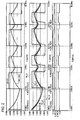
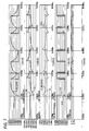
- FIG. 2 is a graph showing voltages at various portions of the circuits in the timing detection device 1 shown in FIG. 1 .
- the signal voltage (Drive) based on a transmitted pulse signal (D_TX) and delivered from the transmitting circuit 21 has a square waveform
- the signal voltage i.e., a pulse signal
- the thresholds (TH_P and TH_N) are indicated by broken lines.
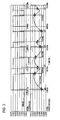
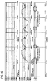
- FIG. 3 is a graph showing the rising timing and the falling timing of the received pulse signal (D_RX).
- the threshold (TH_P) indicates a voltage higher than the negative peak value of the received input signal voltage (Receive) by a constant level.
- the threshold (TH_N) indicates a voltage lower than the positive peak value of the input signal voltage (Receive) by a constant level.
- the rising timing and the falling timing of the received pulse signal (D_RX) are each detected at the time when the input signal voltage (Receive) is attenuated from the peak value by the constant level (more specifically, at the time when the input signal voltage (Receive) is higher than the negative peak value by the constant level or is lower than the positive peak value by the constant level).
- the received pulse signal (D_RX) is generated while being delayed from the transmitted pulse signal (D_TX) by a nearly constant delay time and that the received pulse signal (D_RX) properly reflects the changing points and the pulse widths of the transmitted pulse signal(D_TX).
- the edges of the transmitted waveform are detected using the peaks of the input signal voltage (Receive). More specifically, the level of each of the thresholds is made variable and dynamically set to a level slightly returned from the level of the immediately preceding peak. Hence, the variation in pulse detection delay is suppressed drastically, and the pulse widths of the transmitted pulse signal (D_TX) are accurately reflected to the pulse widths of the received pulse signal (D_RX). As a result, the influence due to the deformation of the signal waveform in the transmission line is excluded. For example, even if a simple serial data sequence is transmitted and received, data can be transferred accurately.
- pulses (pulse widths) on the transmission side can be reproduced accurately from a received waveform having been significantly distorted, even when inexpensive base band communication is used, communication can be carried out at a speed higher than that attained conventionally or over a distance longer that attained conventionally.
- a timing detection device according to Embodiment 2 will be described below.
- the timing detection device 1 according to Embodiment 1 operates precisely, the timing detection device 1 has, for example, two peak hold circuits and two comparators, thereby being complicated and high in cost.
- a timing detection device according to Embodiment 2 accomplishes an operation similar to that of the timing detection device 1 according to Embodiment 1 by using a circuit simpler than that of the timing detection device 1.
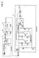
- FIG. 4 is a view showing the configuration of the timing detection device according to Embodiment 2.
- the input signal voltage (Receive) is not input directly to a comparator 52, but the DC offset thereof is cut off using a coupling capacitor C_cpI.
- a clamper circuit 51 is used to hold the voltage (S_Receive) inside the coupling capacitor C_cpI at around the center potential (2.5 V) of the amplitude of the voltage.
- the clamp potential is 2.5 V
- the forward voltage (Vf) of the diodes of the clamper circuit 51 is constant, 0.6 V, for example, the potentials (V01 and V02) inside the clamper circuit 51 should only be set to 2.5 ⁇ 0.6 V.
- the voltage limiting direction of the clamper circuit 51 is switched by controlling a switch SW01 using a feedback signal voltage (FB) from the comparator 52 and by controlling a switch SW11 using the inverted output of the comparator 52.
- FB feedback signal voltage
- switching is performed between the threshold level (TH) in the case of detecting the rising edge of a pulse and the threshold level (TH) in the case of detecting the falling edge of the pulse by applying positive feedback from the output terminal to the positive input terminal of the comparator 52.
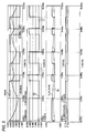
- FIG. 5 is a graph showing voltages at various portions of the circuit of the timing detection device 5.
- the voltage (S_Receive) inside the coupling capacitor C_cpI is clamped at approximately 2.5 V by the operation of the clamper circuit 51.
- the voltage (S_Receive) changes promptly and reaches the positive terminal voltage of the comparator 52.
- the voltage obtained by dividing the output voltage of the comparator 52 by the resistance of a resistor R2 and the resistance of a resistor R3 determines the difference between the peak value and the threshold voltage (TH).
- the output of the comparator 52 is switched, whereby the received pulse signal (D_RX) is switched. Since the received pulse signal (D_RX) is switched in a short time in response to the switching of the transmitted pulse signal (D_TX), the pulse widths of the transmitted pulse signal (D_TX) are accurately reflected to the pulse widths of the received pulse signal (D_RX).
- the voltage variation width inside the capacitor C_cpI is suppressed by extracting the change of the input signal voltage (Receive) as the voltage (S_Receive), whereby the circuit of the timing detection device 5 is simplified.
- the capacitor C_cpI is provided with a function of absorbing the DC offsets of the input signal voltage (Receive) and the voltage (Drive) depending on the amplitude of the input signal voltage (Receive).
- a timing detection device according to Embodiment 3 will be described below.
- the pulses of the signal can be detected securely.
- the timing detection device according to Embodiment 2 is suited in the case that the waveform of the signal is large to the extent that the forward voltage Vf of the diodes of the clamper circuit is regarded as constant.
- the timing detection device according to Embodiment 3 is intended to make up for this kind of shortcoming so as to be usable for receiving pulses having low signal levels, in spite of the simple configuration of the device.
- FIG. 6 is a view showing the configuration of a timing detection device 6 according to Embodiment 3.
- FIG. 7 is a view showing the operation of the timing detection device 6, showing the voltages at various portions of the circuit thereof and the currents flowing through a capacitor Cs and a resistor R_FB2.
- the timing detection device 6 As shown in FIG. 6 , the timing detection device 6 according to Embodiment 3 is equipped with a clamper circuit 61 and a comparator 62.
- the capacitor C_cpI thereof functions as in the case of Embodiment 2.
- the clamper circuit 61 of the timing detection device 6 is equipped with a diode switch formed of a diode D1, a diode D2, a diode D3 and a diode D4.
- the direction of the clamp current of the clamper circuit 61 is switched depending on a slight difference between the middle point between the diode D1 and the diode D2, i.e., the voltage (S_Receive), and the middle point between the diode D3 and the diode D4, i.e., 2.5 V.
- the clamper circuit 61 operates so that the voltage (S_Receive) is precisely controlled to 2.5 V.
- the clamper circuit 61 operates only in one direction, and the direction at the time when the rising edge is detected is opposite to the direction at the time when the falling edge is detected, as in the case of Embodiment 2.
- the operation switching of the clamper circuit 61 is based on a feedback signal voltage (FB).
- the feedback signal voltage (FB) is obtained by giving a delay due to a delay circuit U1 to the output signal (Out) of the comparator 62. This delays the time at which a speeding-up circuit formed of a capacitor Cs and resistors R_FB1 and R_FB2 operates, thereby being effective in preventing excessive compensation for the change in the voltage (S_Receive).
- the threshold level (TH) is generated by dividing the feedback signal voltage (FB) by the resistance of a resistor R2 and the resistance of a resistor R3 and is switched depending on the switching of the feedback signal voltage (FB).
- the delay circuit U1 herein operates as a delay unit.
- the timing detection device 6 even in the case that the amplitude of the input signal voltage (Receive) is small (in the case that the amplitude is approximately 1 V, for example), the difference between the rising timing of the transmitted pulse signal (D_TX) and the rising timing of the received pulse signal (D_RX) is constant, and the difference between the falling timing of the transmitted pulse signal (D_TX) and the falling timing of the received pulse signal (D_RX) is constant. As a result, the pulse widths can be detected accurately.
- FIG. 8 is a view showing the configuration of a receiver incorporating the timing detection device according to the present invention.
- a receiver 10 is equipped with the timing detection device 1, 5 or 6 according to Embodiment 1, 2 or 3 and a base-band demodulator circuit 10a for performing demodulation on the basis of the received pulse signal (D_RX) output from the timing detection device 1, 5 or 6.
- the signal output from the base-band modulator circuit 20a of a transmitter 20 is transferred to the receiver 10 via a transmission line and demodulated by the base-band demodulator circuit 10a.
- the applicable scope of the present invention is not limited to the above-mentioned embodiments.
- the present invention is widely applicable to timing detection devices for detecting the timing at which the value of a received signal is switched on the basis of the received signal.
Landscapes
- Engineering & Computer Science (AREA)
- Computer Networks & Wireless Communication (AREA)
- Signal Processing (AREA)
- Physics & Mathematics (AREA)
- Nonlinear Science (AREA)
- Power Engineering (AREA)
- Dc Digital Transmission (AREA)
- Manipulation Of Pulses (AREA)
- Arrangements For Transmission Of Measured Signals (AREA)
- Measurement Of Unknown Time Intervals (AREA)
- Investigating Or Analyzing Materials By The Use Of Ultrasonic Waves (AREA)
Applications Claiming Priority (1)
| Application Number | Priority Date | Filing Date | Title |
|---|---|---|---|
| JP2009213393A JP4911209B2 (ja) | 2009-09-15 | 2009-09-15 | タイミング検出装置 |
Publications (2)
| Publication Number | Publication Date |
|---|---|
| EP2296306A2 true EP2296306A2 (de) | 2011-03-16 |
| EP2296306A3 EP2296306A3 (de) | 2012-03-28 |
Family
ID=42790515
Family Applications (1)
| Application Number | Title | Priority Date | Filing Date |
|---|---|---|---|
| EP10176723A Withdrawn EP2296306A3 (de) | 2009-09-15 | 2010-09-15 | Vorrichtung zur Takterkennung |
Country Status (5)
| Country | Link |
|---|---|
| US (1) | US8531177B2 (de) |
| EP (1) | EP2296306A3 (de) |
| JP (1) | JP4911209B2 (de) |
| CN (1) | CN102025349B (de) |
| SG (1) | SG169955A1 (de) |
Families Citing this family (5)
| Publication number | Priority date | Publication date | Assignee | Title |
|---|---|---|---|---|
| US9160394B2 (en) * | 2012-02-01 | 2015-10-13 | Sony Corporation | Data reproduction circuit and data transmission device |
| JP5983515B2 (ja) * | 2013-04-18 | 2016-08-31 | 株式会社デンソー | 制御システム |
| US9897630B2 (en) * | 2014-07-09 | 2018-02-20 | Stmicroelectronics S.R.L. | Method of interfacing an LC sensor and related system |
| EP3667935B1 (de) * | 2018-12-14 | 2021-06-16 | Nxp B.V. | Verfahren und system zum betrieb einer kommunikationsvorrichtung, die mittels induktiver kopplung kommuniziert |
| CN116125148A (zh) * | 2022-12-23 | 2023-05-16 | 天津兆讯电子技术有限公司 | 一种脉冲信号宽度检测电路及芯片 |
Citations (3)
| Publication number | Priority date | Publication date | Assignee | Title |
|---|---|---|---|---|
| JPS6471316A (en) | 1987-09-11 | 1989-03-16 | Nec Corp | Pulse reception circuit |
| EP0611059A2 (de) * | 1993-01-21 | 1994-08-17 | Gennum Corporation | System zur Wiedergewinnung der Gleichstromkomponente seriell übertragener Binärsignale |
| US6377108B1 (en) * | 2000-08-28 | 2002-04-23 | Intel Corporation | Low jitter differential amplifier with negative hysteresis |
Family Cites Families (11)
| Publication number | Priority date | Publication date | Assignee | Title |
|---|---|---|---|---|
| US3838448A (en) * | 1973-02-07 | 1974-09-24 | Control Data Corp | Compensated baseline circuit |
| US3947769A (en) * | 1974-10-23 | 1976-03-30 | Hoffman Electronics Corporation | Threshold correction system in FSK transmissions |
| US4888790A (en) * | 1987-10-14 | 1989-12-19 | National Semiconductor Corp. | Timing recovery system using bipolar-pattern center estimator |
| JPH0454791A (ja) * | 1990-06-25 | 1992-02-21 | Toshiba Corp | 変調装置 |
| JP2810592B2 (ja) * | 1992-07-06 | 1998-10-15 | シャープ株式会社 | ディジタル情報再生装置 |
| JP3022182B2 (ja) * | 1994-07-28 | 2000-03-15 | 三洋電機株式会社 | 映像信号処理装置 |
| JPH1038931A (ja) * | 1996-07-30 | 1998-02-13 | Yazaki Corp | センサ信号処理装置 |
| JP4099588B2 (ja) * | 2004-01-14 | 2008-06-11 | ソニー株式会社 | ディフェクト信号生成回路及び同回路を有する光ディスク再生装置 |
| JP4568205B2 (ja) * | 2005-10-14 | 2010-10-27 | 株式会社東芝 | 受信装置 |
| JP4684919B2 (ja) * | 2006-03-03 | 2011-05-18 | ルネサスエレクトロニクス株式会社 | スペクトラム拡散クロック制御装置及びスペクトラム拡散クロック発生装置 |
| JP5223497B2 (ja) * | 2008-06-27 | 2013-06-26 | 富士通セミコンダクター株式会社 | ピークホールド回路 |
-
2009
- 2009-09-15 JP JP2009213393A patent/JP4911209B2/ja not_active Expired - Fee Related
-
2010
- 2010-09-14 CN CN201010282478.XA patent/CN102025349B/zh not_active Expired - Fee Related
- 2010-09-15 EP EP10176723A patent/EP2296306A3/de not_active Withdrawn
- 2010-09-15 SG SG201006697-5A patent/SG169955A1/en unknown
- 2010-09-15 US US12/882,727 patent/US8531177B2/en not_active Expired - Fee Related
Patent Citations (3)
| Publication number | Priority date | Publication date | Assignee | Title |
|---|---|---|---|---|
| JPS6471316A (en) | 1987-09-11 | 1989-03-16 | Nec Corp | Pulse reception circuit |
| EP0611059A2 (de) * | 1993-01-21 | 1994-08-17 | Gennum Corporation | System zur Wiedergewinnung der Gleichstromkomponente seriell übertragener Binärsignale |
| US6377108B1 (en) * | 2000-08-28 | 2002-04-23 | Intel Corporation | Low jitter differential amplifier with negative hysteresis |
Also Published As
| Publication number | Publication date |
|---|---|
| EP2296306A3 (de) | 2012-03-28 |
| US20110062943A1 (en) | 2011-03-17 |
| JP4911209B2 (ja) | 2012-04-04 |
| CN102025349A (zh) | 2011-04-20 |
| SG169955A1 (en) | 2011-04-29 |
| CN102025349B (zh) | 2015-02-18 |
| JP2011066520A (ja) | 2011-03-31 |
| US8531177B2 (en) | 2013-09-10 |
Similar Documents
| Publication | Publication Date | Title |
|---|---|---|
| US8531177B2 (en) | Timing detection device | |
| EP3039942B1 (de) | Adaptive hüllkurvenextraktionsvorrichtung, signaldecodierungsvorrichtung und kontaktlose vorrichtung zur kommunikation über kurze entfernungen mit der adaptiven hüllkurvenextraktionsvorrichtung sowie verfahren dafür | |
| US7817762B2 (en) | Method and apparatus for detecting leading pulse edges | |
| US10651752B1 (en) | Flyback converter with reliable pulse-based isolated communication | |
| US5724002A (en) | Envelope detector including sample-and-hold circuit controlled by preceding carrier pulse peak(s) | |
| CN111564975B (zh) | 一种用于反激式转换器的接收器及其控制方法 | |
| EP3107208B1 (de) | Demodulatorschaltung und verfahren zur demodulation | |
| KR940005386B1 (ko) | 통신 시스템의 신호 분산 특성을 결정하기 위한 장치 및 방법 | |
| US8179148B2 (en) | Information detecting apparatus and method | |
| US9203520B2 (en) | Detecting apparatus, optical receiving apparatus, detecting method, and optical receiving method | |
| US20100260283A1 (en) | Duty-cycle modulated transmission | |
| CN107919859B (zh) | 基于过载状况的持续时间来控制放大器增益的自动增益控制(agc)电路和方法 | |
| US5933458A (en) | Circuit for processing asynchronous signals having periodic synchronization bursts | |
| EP0715439A2 (de) | Entscheidungsvorrichtung für Empfänger mit Burst-Modus | |
| JP2009212924A (ja) | バーストモード自動利得制御回路 | |
| WO2003039060A2 (en) | Apparatus and method to generate an adaptive threshold for a data slicer | |
| US6188264B1 (en) | Automatic threshold level control circuit | |
| JP6769961B2 (ja) | Am復調 | |
| US20050211878A1 (en) | Receiver circuit for a push-pull transmission method | |
| US10057092B1 (en) | Transmitter for transmitting packets and method thereof | |
| US20080157749A1 (en) | Method and receiver for estimating dc offset | |
| JP2012085229A (ja) | Ponシステムとその局側装置及び光受信器並びに光受信方法 | |
| US6034802A (en) | Wireless communications systems with self threshold setting | |
| JP3833259B2 (ja) | Fsk受信器における周波数制御信号の生成 | |
| JP2520378Y2 (ja) | 受光回路 |
Legal Events
| Date | Code | Title | Description |
|---|---|---|---|
| PUAI | Public reference made under article 153(3) epc to a published international application that has entered the european phase |
Free format text: ORIGINAL CODE: 0009012 |
|
| AK | Designated contracting states |
Kind code of ref document: A2 Designated state(s): AL AT BE BG CH CY CZ DE DK EE ES FI FR GB GR HR HU IE IS IT LI LT LU LV MC MK MT NL NO PL PT RO SE SI SK SM TR |
|
| AX | Request for extension of the european patent |
Extension state: BA ME RS |
|
| PUAL | Search report despatched |
Free format text: ORIGINAL CODE: 0009013 |
|
| AK | Designated contracting states |
Kind code of ref document: A3 Designated state(s): AL AT BE BG CH CY CZ DE DK EE ES FI FR GB GR HR HU IE IS IT LI LT LU LV MC MK MT NL NO PL PT RO SE SI SK SM TR |
|
| AX | Request for extension of the european patent |
Extension state: BA ME RS |
|
| RIC1 | Information provided on ipc code assigned before grant |
Ipc: H03K 5/1252 20060101ALN20120222BHEP Ipc: H04L 7/033 20060101ALN20120222BHEP Ipc: H04L 25/06 20060101AFI20120222BHEP |
|
| 17P | Request for examination filed |
Effective date: 20120928 |
|
| 17Q | First examination report despatched |
Effective date: 20170214 |
|
| STAA | Information on the status of an ep patent application or granted ep patent |
Free format text: STATUS: THE APPLICATION IS DEEMED TO BE WITHDRAWN |
|
| 18D | Application deemed to be withdrawn |
Effective date: 20180223 |