EP2296442A1 - Dispositif d'affichage électroluminescent organique et son procédé de fabrication - Google Patents
Dispositif d'affichage électroluminescent organique et son procédé de fabrication Download PDFInfo
- Publication number
- EP2296442A1 EP2296442A1 EP09754421A EP09754421A EP2296442A1 EP 2296442 A1 EP2296442 A1 EP 2296442A1 EP 09754421 A EP09754421 A EP 09754421A EP 09754421 A EP09754421 A EP 09754421A EP 2296442 A1 EP2296442 A1 EP 2296442A1
- Authority
- EP
- European Patent Office
- Prior art keywords
- linear
- ink
- banks
- organic light
- substrate
- Prior art date
- Legal status (The legal status is an assumption and is not a legal conclusion. Google has not performed a legal analysis and makes no representation as to the accuracy of the status listed.)
- Granted
Links
Images


Classifications
-
- H—ELECTRICITY
- H10—SEMICONDUCTOR DEVICES; ELECTRIC SOLID-STATE DEVICES NOT OTHERWISE PROVIDED FOR
- H10K—ORGANIC ELECTRIC SOLID-STATE DEVICES
- H10K71/00—Manufacture or treatment specially adapted for the organic devices covered by this subclass
- H10K71/10—Deposition of organic active material
- H10K71/12—Deposition of organic active material using liquid deposition, e.g. spin coating
- H10K71/13—Deposition of organic active material using liquid deposition, e.g. spin coating using printing techniques, e.g. ink-jet printing or screen printing
- H10K71/135—Deposition of organic active material using liquid deposition, e.g. spin coating using printing techniques, e.g. ink-jet printing or screen printing using ink-jet printing
-
- H—ELECTRICITY
- H10—SEMICONDUCTOR DEVICES; ELECTRIC SOLID-STATE DEVICES NOT OTHERWISE PROVIDED FOR
- H10K—ORGANIC ELECTRIC SOLID-STATE DEVICES
- H10K59/00—Integrated devices, or assemblies of multiple devices, comprising at least one organic light-emitting element covered by group H10K50/00
- H10K59/10—OLED displays
- H10K59/12—Active-matrix OLED [AMOLED] displays
- H10K59/1201—Manufacture or treatment
-
- H—ELECTRICITY
- H10—SEMICONDUCTOR DEVICES; ELECTRIC SOLID-STATE DEVICES NOT OTHERWISE PROVIDED FOR
- H10K—ORGANIC ELECTRIC SOLID-STATE DEVICES
- H10K59/00—Integrated devices, or assemblies of multiple devices, comprising at least one organic light-emitting element covered by group H10K50/00
- H10K59/10—OLED displays
- H10K59/12—Active-matrix OLED [AMOLED] displays
- H10K59/122—Pixel-defining structures or layers, e.g. banks
-
- H—ELECTRICITY
- H10—SEMICONDUCTOR DEVICES; ELECTRIC SOLID-STATE DEVICES NOT OTHERWISE PROVIDED FOR
- H10K—ORGANIC ELECTRIC SOLID-STATE DEVICES
- H10K59/00—Integrated devices, or assemblies of multiple devices, comprising at least one organic light-emitting element covered by group H10K50/00
- H10K59/30—Devices specially adapted for multicolour light emission
- H10K59/35—Devices specially adapted for multicolour light emission comprising red-green-blue [RGB] subpixels
-
- H—ELECTRICITY
- H10—SEMICONDUCTOR DEVICES; ELECTRIC SOLID-STATE DEVICES NOT OTHERWISE PROVIDED FOR
- H10K—ORGANIC ELECTRIC SOLID-STATE DEVICES
- H10K71/00—Manufacture or treatment specially adapted for the organic devices covered by this subclass
Definitions
- the present invention relates to a method of manufacturing an organic electroluminescent (EL) display. More particularly, the invention relates to a method of manufacturing an organic EL display in which an organic light-emitting layer is formed by a coating method (more specifically by an ink jet method).
- Organic EL displays can be broadly classified, according to methods with which their organic light-emitting layers are formed, into the following two types.
- One type employs a method of forming an organic light-emitting layer by deposition, which is used in the case where the organic light-emitting layer is made of a low-molecular-weight organic material.
- the other type employs a method of forming an organic light-emitting layer by a solvent coating method, which is often used in the case where the organic light-emitting layer is made of a polymeric organic material as well as a low-molecular-weight organic material.
- an organic light-emitting layer by a solvent coating method there is a method of discharging droplets of ink containing an organic light-emitting material into pixel regions of a display substrate using an ink jet device to form an organic light-emitting layer (see Patent Document 1). In the discharged droplet, an organic light-emitting material and a solvent are included.
- the ink jet device includes an ink jet head having two or more nozzles. While controlling a positional relationship between the nozzles of the ink jet head and the display substrate, the ink jet device discharges ink from the nozzles. It is known that there are variations in size among droplets discharged from nozzles that the ink jet head has (see Patent Document 2). Reported in Patent Document 2 is a technique of causing a plurality of droplets to land on one pixel region and adjusting the landing position of each droplet, thereby improving film uniformity in the pixel region.
- a pixel region of a display substrate into which droplets are discharged is often defined by a partition, referred to as a "bank". This is for the purpose of causing discharged ink to position-selectively remain in the pixel region.
- a plurality of pixels are arranged on the substrate in rows of respective colors (R, G or B) such that they form a stripe pattern.
- R, G or B respective colors
- a method of discharging droplets while causing an ink jet head of an ink jet device to scan in a direction perpendicular to the longitudinal direction of the stripe is known (see Patent Documents 4 to 6).
- banks may define a linear region including a group of pixels of the same color (for example, R: red, G: green, or B: blue) arranged in a row, among pixels arranged in the form of stripes (see Patent Document 3).
- the bank that defines the linear region may be referred to as a "linear bank”. That is, an organic light-emitting layer of R, G or B is formed in every region (hereinafter also referred to as a "linear region”) defined by the linear bank.
- the relative movement of the ink jet head in parallel to the line direction of the linear banks prevents ink to be applied into one linear region from erroneously intruding into the adjacent linear region. That is, in a color display, for example, a linear region in which an R organic light-emitting layer is formed, a linear region in which a G organic light-emitting layer is formed, and a linear region in which a B organic light-emitting layer is formed are repeatedly arranged, so that a stripe pattern is formed. Therefore, ink containing an organic light-emitting material must be reliably prevented from leaking into the adjacent linear region to cause color mixture. For this purpose, ink is discharged while an ink jet head is relatively moved in parallel to the line direction of the linear banks.
- droplets are always discharged from the same nozzles into one linear region defined by linear banks. That is, for every region defined by linear banks, its corresponding nozzles that supply (discharge) droplets into the region is set.
- the amount of supplied ink slightly differs from one region defined by linear banks to another.
- the difference in amount of supplied ink causes formed organic light-emitting layers to have different thicknesses; the difference in thickness among organic light-emitting layers leads to differences in amount of emitted light, intensity of emitted light and wavelength of emitted light.
- An object of the invention is to suppress non-uniformity in thickness of an organic light-emitting layer from one line to another even when an organic light-emitting layer is formed on a display substrate having linear banks by applying ink onto the substrate using ink jetting with an ink jet head having non-uniformity of nozzles. This allows an organic EL display having high image quality without streaks to be manufactured. Further, an object of a preferred aspect of the invention is to provide a method of manufacturing a high definition organic EL display in which color mixture is suppressed.
- a first aspect of the invention relates to a method of manufacturing an organic EL display as follows.
- a second aspect of the invention relates to an organic EL display as follows.
- organic light-emitting layers are formed on a display substrate having linear banks by an ink jet method, variations in thickness of the organic light-emitting layer from one linear region to another can be suppressed. An organic EL display without luminance unevenness is therefore obtained. Further, according to a preferred method of the invention, a high definition organic EL display in which color mixture is suppressed is obtained.
- An organic EL display manufactured by the invention has two or more linear banks arranged in parallel to each other.
- the linear bank may be forward tapered or reverse tapered, and preferably forward tapered.
- the material for a first bank may be any material as long as it has insulating properties; however it is preferable that the material be an insulating resin (such as polyimide).
- the surface of the linear bank may be subjected to a fluoridation process using fluorine gas plasma or the like to reduce its wettability.
- the line direction of the linear bank may be any direction.
- the linear bank is in parallel to the short axis direction of a display or in parallel to its long axis direction.
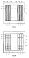
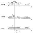
- FIG.2A shows a state of an organic EL display in which a cathode electrode and the like are omitted to expose organic light-emitting layers.
- R organic light-emitting layer 15R, G organic light-emitting layer 15G or B organic light-emitting layer 15B is formed in each linear region 12, and they are repeatedly arranged (forming a stripe pattern). It is preferable that the thickness of an organic light-emitting layer be from about 50 to 100 nm (for example, 60 nm).
- FIG.2B shows a state in which organic light-emitting layers 15R, 15G, and 15B are omitted to expose pixel region 13.
- two or more pixel regions 13 are arranged in rows in linear region 12.
- Pixel regions 13 are not independently partitioned so that a liquid in the each pixel is not interfere with movement to adjacent pixel.
- Pixel regions 13 are linked to one another so that the liquid can move among them through gaps 17. In other words, ink discharged into linear region 12 can freely move in linear region 12.
- each pixel region 13 at least a pixel electrode (typically an anode electrode) is arranged.
- an anode electrode In the case of employing an active type, an anode electrode is independently arranged in every pixel region while in the case of employing a passive type, anode electrodes are arranged in a stripe pattern.
- an anode electrode In the case of employing bottom emission, an anode electrode needs to be a transparent electrode, and may be an indium-tin-oxide (ITO) electrode or the like.
- ITO indium-tin-oxide
- an anode electrode In the case of employing top emission, an anode electrode is preferably a reflecting electrode, and may be a silver electrode, a silver-palladium-copper alloy (also referred to as "APC”) electrode or the like.
- an anode electrode In the case of employing an active type, an anode electrode is connected to a drain electrode of a thin film transistor (TFT).
- TFT thin film transistor
- a hole transport layer and an electron blocking layer may be arranged on and above the anode electrode.
- the hole transport layer is a layer made of a hole transfer material.
- the materials for the hole transport layer may be oxide such as WO x (tungsten oxide), MoO x (molybdenum oxide) or VO x (vanadium oxide), or a combination of these materials.
- the hole transfer material may be poly(3,4-ethylenedioxythiophene) doped with polyethylene sulfonate (referred to as "PEDOT-PSS”), or its derivative (such as copolymer).
- the thickness of a hole transport layer is typically 10 nm or more and 100 nm or less, and can be about 30 nm.
- the electron blocking layer has a role that blocks electrons from being transported to the hole transport layer and a role that transports holes to an organic light-emitting layer with efficiency, and is made of, for example, a polyaniline material.
- the thickness of an electron blocking layer is typically 10 nm or more and 100 nm or less, and can be about 40 nm.
- the organic light-emitting layer is arranged over the whole linear region including two or more pixel regions aligned in a row. That is, the organic light-emitting layer extends over two or more pixel regions aligned in a row.
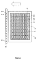
- a method of manufacturing an organic EL display panel according to the invention includes 1) preparing a display substrate before organic light-emitting layers are formed (see FIG.2B ), 2) arranging an ink jet head beside the prepared display substrate, and 3) applying ink containing an organic light-emitting material by ink jetting to form an organic light-emitting layer.
- the display substrate before forming organic light-emitting layers is, for example, the substrate shown in FIG.2B , and includes a substrate, a plurality of linear banks in parallel to each other, and a plurality of pixel regions arranged in linear regions sandwiched between the linear banks.
- pixel regions 13 at this point for example, anode electrodes are exposed, hole injection transport layers are exposed, or electron blocking layers are exposed.
- the organic light-emitting material contained in ink is preferably a polymeric luminescent material
- examples of the polymeric luminescent material include poly phenylene vinylene (PPV) and its derivatives, poly acetylene and its derivatives, polyphenylene and its derivatives, poly para phenyleneethylene and its derivatives, poly 3-hexyl thiophene (P3HT) and its derivatives, poly fluorene (PF) and its derivatives, and the like.
- the ink jet head is arranged beside the substrate. Specifically, the ink jet head is arranged in a side with respect to the line direction of the linear banks, and more specifically in a side with respect to the line direction of a linear bank at the farthest end among a plurality of linear banks.
- the alignment direction of nozzles of the arranged ink jet may be in parallel to the line direction of linear banks of the substrate (see FIG.3 ).
- a distance from nozzle 21-1 at one end to nozzle 21-n at the other end be equal to or greater than the length in the line direction of linear region 12 of substrate 10. This is because ink can be applied over the whole linear region 12 at a time.
- the alignment direction of nozzles 21 of ink jet head 20 is inclined with respect to the line direction of linear region 12, it is preferable that "the component in the foregoing line direction of the distance from nozzles 21-1 to nozzle 21-n" be equal to or greater than the length in the line direction of linear region 12.
- ink jet head 20 may be arranged so as to be inclined with respect to the line direction. This can decrease the pitch of droplet landing in one linear region, enabling the time required for leveling to be reduced.
- the inclining of ink jet head 20 causes time differences in landing of droplets on the same linear region. Therefore, an ink droplet that has first landed on a region dries and increases its viscosity until the final ink droplet lands on the region, which interferes with leveling after droplets are connected.
- a plurality of ink jet heads (20-1 to 20-6) may be arranged so as to be each inclined with respect to the line direction.
- ink in this way allows ink discharged from all nozzles to be leveled in the linear region even if there are variations in discharge caused by size variations among nozzles. Variations in applied film thickness can therefore be suppressed.
- ink amount corresponding to the desired film thickness it is not necessarily required for ink amount corresponding to the desired film thickness to be applied in a single scan.
- the applying of ink to the whole linear region 12 may be completed by repeating scanning a plurality of times. If ink is applied by repeating scanning a plurality of times, however, the viscosity of the ink applied in the former scanning may increase to suppress leveling in its connection portion with ink applied in the latter scanning. Therefore, in the case of using a solvent that easily evaporates, such as ink solvent of an organic light-emitting material, it is desirable that ink be applied over the whole linear region in a single scan.
- the pitch between nozzles 21 arranged in a row in ink jet head 20 be from 10 to 50 ⁇ m, and be, for example, about 20 ⁇ m. This is for the purpose of causing ink discharged from nozzles 21 to be mutually connected at the point on which the ink lands. It is also preferable that the amount of ink per droplet of the droplets discharged from nozzles 21 be from 1 to 15 pl, and be, for example, 3 pl.
- droplets land also on gap 17 between the pixel regions shown in FIG.2B .
- the landing of droplets on gap 17 makes it possible to connect ink of the pixel regions to level them with reliability, even though wettability of pixel regions 12 differ from that of gap 17 between the pixel regions.
- an electron blocking layer be provided in the whole linear region before a light-emitting layer is applied to make the wettability of pixel regions 12 equal to the wettability of gap 17 between the pixel regions. As a result, ink of the pixel regions can be connected with reliability to improve leveling.
- the height of gap 17 between the pixel regions be greater to some extent than the height of pixel regions 13.
- the difference in height is set so as not to be too large, and the applied film immediately after the applying of ink covers gap 17 so as to avoid interfering with leveling.
- ink is concentrated into pixel region 13 in a drying process to effectively use an ink material.
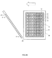
- ink jet head 20 is moved relatively with respect to display substrate 10 in a direction perpendicular to the line direction of linear banks 11 of display substrate 10.
- Ink jet head 20 may be moved, or substrate 10 may be transported, or both of them may be moved.
- nozzles 21 of ink jet head 20 reach one of linear regions 12 (see FIG.4 ), droplets of ink are discharged from nozzles 21.
- the amount of applied ink is from 100 to 500 pl per pixel.
- a plurality of droplets may be discharged from one nozzle into one pixel, thereby supplying the required amount of ink.
- the discharged droplets of ink land on linear region 12.
- the amount of droplets discharged from nozzles 21 of ink jet head 20 may differ from one nozzle to another.
- the thickness of the applied film is made uniform (leveled) in linear region 12. Therefore, even though there is a difference among the amounts of droplets from nozzles 21, the applied film in linear region 12 is made uniform.
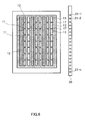
- ink jet head 20 Upon completion of discharging of droplets of ink into one linear region 12, ink jet head 20 is further relatively moved so as to move nozzles 21 of ink jet head 20 to next linear region 12 into which droplets of ink are to be discharged (see FIG. 5 ).
- R ink, G ink and B ink are applied by their respective individual scans, and therefore droplets of ink are discharged into every three linear regions.
- nozzles 21 reach desired linear region 12, droplets of ink are discharged again to cause the droplets to land on linear region 12. This is repeated to apply ink to all linear regions 12 into which the ink is to be applied (see FIG.6 ).
- ink is supplied into every linear region 12 in succession in this way, all the linear regions are coated by discharging from the same nozzles. The same amount of ink can therefore be supplied to all linear regions 12. In other words, variations in thickness of the applied film from one linear region to another are reduced. Consequently, streaks can be prevented from occurring when the regions constitute a display.
- the other color ink is applied in the same way as mentioned above, so that ink of all of R, G and B is applied.
- the line direction of the linear banks of an organic EL display according to the invention may be in parallel to the short axis direction of the display, or may also be in parallel to the long axis direction. If the line direction of the linear banks is in parallel to the short axis direction, an ink jet head for scanning can be made in a smaller size. In the case where light emission unevenness slightly occurs because of variations in nozzles, the light emission unevenness occurs in a small region and therefore is not conspicuous. On the other hand, if the line direction of the linear banks is in parallel to the long axis direction, the scanning distance of an ink jet head is shortened. This enables coating to be completed in a short time to improve productivity, and also enables drying unevenness during coating to be suppressed.
- ink is supplied into every linear region 12 in succession as described above, a risk of erroneously mixing ink into the adjacent linear region increases, while variations in thickness of the applied film from one linear region to another are reduced.
- the mixture of ink into the adjacent linear region causes color mixture, remarkably reducing the image quality as a display.
- the speed of relative movement of the ink jet head and the substrate is increased in order to increase productivity, the occurrence rate of color mixture increases.
- the relative movement speed e.g., the transport speed of the substrate
- the relative movement speed is decreased so as to cause droplets discharged from nozzles to land on the linear region with reliability.
- the relative movement speed be increased to increase productivity.
- the relative movement speed (preferably the transport speed of the substrate) when droplets are discharged is preferably from 50 to 300 mm/s, while the relative movement speed (preferably the transport speed of the substrate) when droplets are not discharged is not particularly limited, and is, for example, 400 mm/s or more.
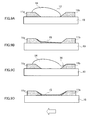
- ink droplet 14 may be landed on the forward side in the transport direction of the substrate (on the rear side in the movement direction of the ink jet head) in linear region 12.
- the ink unevenly distributed in the forward in the transport direction of the substrate naturally spreads toward the rear in the transport direction by wind pressure caused by transport of the substrate, thereby enabling formation of applied film 16 ( FIG.8C ).
- the substrate itself may optionally be tilted so as to raise the forward in the transport direction of the substrate after the ink application.
- the surface tension (wettability) of linear bank 11 may be utilized.
- the wettability of the surface on the side of region 12 of linear bank 11a is equal to the wettability of the surface on the side of region 12 of linear bank 11b.
- the linear bank 11a is forward in the transport direction (see arrow) of substrate 10, and the linear bank 11b is rear in the transport direction of substrate 10.
- an ink droplet that has landed in the forward in the transport direction of the substrate does not spread evenly, and therefore the thickness of organic light-emitting layer 15 is unlikely to become uniform, as shown in FIG.9B .
- linear banks 11 define linear region 12, and the wettability of surface 30 on the side of region 12 of linear bank 11b is higher than the wettability of the surface on the side of region 12 of linear bank 11a.
- the linear bank 11b is rear in the transport direction of the substrate, and the linear bank 11a is forward in the transport direction of the substrate.
- ink can wet and spread over the whole linear region 12 even though an ink droplet lands in the forward in the transport direction of the substrate.
- organic light-emitting layer 15 having a uniform film thickness is obtained as shown in FIG.9D .
- a manufacturing method according to the invention be carried out in this way by combining measures for reliably preventing color mixture.
- ink is discharged to a linear region (including a plurality of pixel regions), it be waited until the thickness of an applied film of the ink is made uniform (leveled), and then a solvent of the ink be removed.
- waiting refers to that the substrate is left in the atmosphere or in an inert gas atmosphere.
- the time for waiting varies mainly depending on the viscosity of ink and the surface tension of the ink with respect to a region to which the ink is applied.
- the viscosity of ink containing an organic light-emitting material to be applied by an ink jet device is from about 5 to 20 cps.
- the surface tension of ink with respect to a region to which the ink is applied is from 20 to 40 dyn/cm.
- FIG.10 Three pixel regions 13 arranged in the region (linear region) defined by the linear banks are assumed (see FIG.10 ).
- a length 1 in FIG.10 is about 1 mm.
- the state in which applied film 16 having ⁇ 100% variations is formed in this region is set as the initial state ( FIG.10A ).
- the time from the initial state to a state in which variations of the applied film is leveled to ⁇ 1% ( FIG.10B ) is obtained.
- the result is shown in a graph of FIG. 11 .
- the vertical axis of the graph in FIG.11 indicates time (sec) required for leveling; and the horizontal axis indicates the viscosity (cps)of ink constituting an applied film.
- Plots of 0 represent results in the case where the surface tension of the applied region is 20 dyn/cm; plots of ⁇ represent results in the case where the surface tension of the applied region is 30 dyn/cm; and plots of ⁇ represent results in the case where the surface tension of the coated region is 40 dyn/cm.
- the waiting time may be affected by evaporation of a solvent from the applied film, and therefore is adjusted in accordance with the actual conditions.
- the solvent is removed from a leveled applied film (drying process). Thereby, an organic light-emitting layer is formed.
- an organic light-emitting layer having a highly uniform thickness is formed in each linear region, and variations in thickness of the organic light-emitting layer among linear regions are reduced.
- an electron injection transport layer, an opposite electrode (typically a cathode electrode) and the like are layered to produce an organic EL device, and further a sealing film, a glass substrate and the like are arranged, thereby manufacturing a display.
- the material of a cathode electrode layer differs depending on whether the display is a bottom emission type or a top emission type.
- the cathode electrode In the case of the top emission type, the cathode electrode needs to be transparent, and therefore it is preferable that an ITO electrode, an indium zinc oxide (IZO) electrode or the like be formed. It is preferable that a buffer layer and the like be formed between the organic light-emitting layer and the cathode electrode layer.
- the cathode electrode need not be transparent, and an electrode made of any material may be used.
- the cathode electrode may be formed on the organic light-emitting layer arranged in each pixel region, and is sometimes formed so as to cover all pixels included in one linear region.
- the cathode electrode is typically formed by a sputtering method or a deposition method. Further, the cathode electrode need not always be separated by linear region. That is, when an anode electrode is controlled independently for every pixel electrode as in an active-matrix type, a TFT element that drives the pixel electrode is independent, and therefore the cathode electrode can be shared among a plurality of linear regions.
- An organic EL display panel of the invention may be sealed by further providing a cover material to a surface on which the cathode electrode is formed. With the cover material, intrusion of moisture and oxygen is suppressed.
- the organic EL display panel of the invention can be manufactured as described above, and can have structural features in a relationship between organic light-emitting layers formed in linear regions by coating and linear banks.
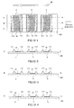
- a first feature of the organic EL display panel of the invention is that the heights of contacts between an organic light-emitting layer arranged in each linear region and linear banks are fixed in the line direction. As shown in FIG.12 , when attention is focused on one linear region (linear region X, Y or Z), the thickness of organic light-emitting layer 15 is fixed in the line direction.
- organic light-emitting layer 15 formed in each linear region (linear region X, Y or Z) in FIG.12-1 a cross-section along the line A-A ( FIG.12-2 ), a cross-section along the line B-B ( FIG.12-3 ), and a cross-section along the line C-C ( FIG.12-4 ) are approximately identical to one another; the heights of contacts between organic light-emitting layer 15 and linear banks 111 are fixed in the line direction.
- the fixed height means that a difference between the minimum height and the maximum height is within 20% (preferably 10%) of the film thickness with a pixel of the organic light-emitting layer serving as the center. This is because according to a method of the invention, there is no large difference in the drying environment for a coating liquid in one linear region.
- the organic EL display panel having banks sometimes deteriorates gradually in its long-term use. It is considered that one of causes of the deterioration is that an outflow from the bank acts on the organic light-emitting layer.
- the outflow from the bank is, for example, moisture and an organic matter containing a hydroxyl group.
- the degree of deterioration of the organic light-emitting layer because of an outflow from the bank is considered to be affected by a positional relationship between the organic light-emitting layer and the bank.
- the distance between pixels adjacent to each other in each linear region is very short. Therefore, when a difference occurs in the degree of deterioration of the pixels to cause a difference in light-emitting characteristic, the difference is visually recognized with ease as light emission unevenness of a display.
- the heights of contacts between the an organic light-emitting layer and linear banks can be fixed in every linear region. Therefore, the degree of progress of long-term deterioration can be the same among organic light-emitting devices included in one linear region. Accordingly, light emission unevenness of a display can be suppressed even in the long-term use.
- a second feature of the organic EL display panel of the invention is as follows.
- the height of contact between an organic light-emitting layer formed in a linear region on one end of a display panel and linear bank are greater than the height of contact between an organic light-emitting layer formed in a linear region on the other end of the display panel and linear banks.
- FIG.12-1 since the drying speed of a coating liquid applied to linear region X in an end on a side (right side) where coating of substrate 100 starts is rapid, organic light-emitting layer 15 formed by drying is likely to be stranded on a side surface of bank 111 (see FIGS.12-2 to 12-4 ).
- the film thickness profile of an organic light-emitting layer in each pixel affects the light-emitting characteristic.
- the heat generation characteristic may be varied. Specifically, since organic light-emitting layer 15 formed in linear region X arranged in one end (on a side where coating starts) of a display panel in FIG.12-1 tends to have a large film thickness distribution, the amount of heat generation of an organic light-emitting device in linear region X is relatively large. On the other hand, since organic light-emitting layer 15 formed in linear region Z arranged in the other end of the display panel has a suppressed film thickness distribution, the amount of heat generation of organic light-emitting device 15 in linear region Z is relatively small.
- the can sealing structure is a structure that puts a sealing can on a display substrate on which an organic light-emitting device is formed, so that the organic light-emitting device is protected from the external environment.
- heat tends to stay inside the sealing can.
- a heat distribution is made uniform by convection.
- moisture and oxygen gas present in the interior of the sealing can move by the flow of heat.
- an adsorbent that absorbs moisture and oxygen gas is arranged at a downstream position, moisture and oxygen gas can be removed with efficiency.
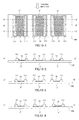
- a third feature of the organic EL display of the invention is that film thickness profiles in the line direction of organic light-emitting layers formed in linear regions are similar to one another. That is, as shown in FIG.14-1 , any one of organic light-emitting layers 15 formed in linear regions is relatively thick at one position (G) in the line direction; it is relatively thin at another position (H) in the line direction (see FIGS.14-2 to 14-4).
- FIG.14-2 is a cross-sectional view taken along the line D-D of FIG.14-1;
- FIG.14-3 is a cross-sectional view taken along the line E-E of FIG.14-1;
- FIG.14-4 is a cross-sectional view taken along the line F-F of FIG.14-1 .
- nozzles of an ink jet head vary in size, and their sizes are not necessarily constant.
- a coating method of the invention droplets simultaneously fall over the whole one linear region, and the thickness of the coated film is made uniform (leveled). Therefore, the thickness of an organic light-emitting layer is made uniform over the whole linear region.
- variations in the sizes of nozzles, variations in the temperatures of nozzles and variations in the drying states of nozzles, which have no influence on light-emitting characteristic are reflected in the thickness of an organic light-emitting layer to cause a distribution of the thickness.
- the organic light-emitting layer of the organic EL display of the invention has a distribution in thickness
- thickness distributions in the line direction of organic light-emitting layers of any linear regions are similar (see FIGS.14-2 to 14-4 ). That is, positions in the line direction of the thickest portions or the thinnest portions of organic light-emitting layers in linear regions are exactly aligned or vary within a distance 2 to 8 times as long as the nozzle pitch. Therefore, even if a stress is applied to a display such that the display is curved in the line direction (bent around an axis perpendicular to the line direction), deformations in the thickness direction in all linear regions are the same. This suppresses damage to organic light-emitting layers.
- FIG.15-1 in organic light-emitting layers 15 formed by providing a coating liquid along the line direction of linear banks, their film thickness profiles in the line direction differ from one linear region to another and are not similar ( FIGS. 15-2 to 15-4 ). That is, FIG.15-2 is a cross-sectional view taken along the line D'-D' of FIG.15-1; FIG.15-3 is a cross-sectional view taken along the line E'-E' of FIG.15-1; FIG.15-4 is a cross-sectional view ( FIG.15-4 ) taken along the line F'-F' of FIG.15-1 .
- the film thickness profiles of any organic light-emitting layers 15 differ from one another.
- the organic EL display panel can be made as a flexible display (e.g., a roll display or a folding display).
- a flexible display for example, it is conceivable to bend the display in parallel with the extending direction of linear banks. If the thickness profile of an organic light-emitting layer in one linear region distinctly differs from the thickness profile of an organic light-emitting layer in another linear region, the organic light-emitting layer in the one linear region is likely to be broken upon bending the display in parallel with the extending direction of linear banks. In a method of coating along the line direction of linear banks, an organic light-emitting layer having a distinctly different thickness profile is sometimes formed because of variations in ink jet nozzles.
- the whole organic light-emitting layer is broken.
- the quality as a display cannot be ensured.
- a coating liquid applied into a linear region is made even. This makes it difficult to form an organic light-emitting layer having a distinctly different thickness profile.
- thickness profiles in the line direction of organic light-emitting layers in linear regions are similar. Therefore, even if each of the organic light-emitting layers has portion having a distinct thickness can be formed, the portions are aligned along the line perpendicular to the line direction. Therefore, the organic light-emitting layer is unlikely to be broken with bending the display in parallel with the extending direction of linear banks.
- Linear banks of the organic EL display of the invention may be formed by a photolithography method, and may also be formed by a printing method.
- Examples of the printing method include a gravure offset printing method.
- a printing method a bank material (e.g., a resin material) placed on the surface of printing cylinder 200, so-called cylinder, is transferred onto substrate 100 to form linear banks 111.
- the shapes of linear banks 111 formed by the printing method are precisely the same in the line direction. That is, variations in shape in the line direction are the same for any linear banks 111.
- ink is applied in each linear region of linear banks formed by a printing method, through leveling of the coating liquid the shape profile of the organic light-emitting layer is hard to be reflected by the variations in shape in the linear bank.
- an organic light-emitting layer is formed by supplying a coating liquid along the line direction of linear banks to each linear region defined by linear banks formed by a printing method, not only the shape profile of the organic light-emitting layer is likely to be reflected by the variations in shape in the linear bank, but also the variations of nozzles of an ink jet head and the shape variations in the line direction of linear banks might be combined together.
- the organic EL display panel of the invention is sometimes provided with a color filter for every pixel in order to increase color purity.
- the color filter is made of a colored layer arranged between linear banks adjacent to each other.
- variations of nozzles of an ink jet head sometimes cause unevenness in the color filter.
- a color filter be formed by coating liquid along the line direction of linear banks. This is for the purpose of suppressing combining of mutual variations.
- a colored layer of the color filter is sometimes applied along linear regions in succession by a dispenser or the like.
- an organic light-emitting layer be formed by coating in a direction perpendicular to the linear banks so that mutual variations are not combined together.
- the cathode electrode of the organic EL display of the invention is sometimes deposited by sputtering.
- ITO which is a transparent electrode
- Sputtering deposition can be performed, for example, using a magnetron sputtering device, which transports a member on which a cathode electrode is to be deposited (a display substrate on which an organic light-emitting device with no cathode electrode) to cause it to pass through a sputter region. Since the environment of the sputter region is not necessarily uniform (with variations), slight streaks can occur along the transport direction in a film formed by sputtering.
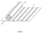
- an organic light-emitting layer is formed by coating liquid along the direction perpendicular to the line direction of linear banks as in the invention, as shown in FIG.17 , when a cathode electrode is deposited by sputtering, it is preferable that substrate 100 be transported along the line direction of linear banks (i.e., the longitudinal direction of organic light-emitting layer 15) to pass through sputter region 300. This is for the purpose of suppressing combining of variations of nozzles of an ink jet head and variations in the sputter region together.
- cathode electrodes of all organic light-emitting pixels can be made conductive.
- the coverage is increased to suppress thinning or cutting of the deposited cathode on the bank. Therefore, conductivity of the cathode electrode can be improved .
- the organic EL display of the invention can have a sealing resin layer that seals an organic light-emitting device formed on a substrate.
- sealing resin can be applied to a display substrate on which an organic light-emitting device is arranged; and placing a sealing substrate (glass substrate) on the display substrate, a gap between the display substrate and the sealing substrate is filled with sealing resin.
- the sealing resin spreads in the gap along the line direction of linear banks. Since the sealing resin spreads along the line direction, streaks in the line direction sometimes occur in the formed sealing resin layer.
- the organic light-emitting layer of the organic EL display of the invention is formed by coating liquid along the direction perpendicular to the line direction of linear banks, and therefore streaks in the line direction are unlikely to occur. Therefore, light emission unevenness due to streaks in the foregoing sealing resin can be suppressed.
- the organic light-emitting layer formed by providing a coating liquid along the line direction of linear banks streaks in the line direction are likely to occur. Therefore, there is a potential of emphasizing light emission unevenness in combination with streaks of the foregoing sealing resin.
Landscapes
- Engineering & Computer Science (AREA)
- Manufacturing & Machinery (AREA)
- Microelectronics & Electronic Packaging (AREA)
- Electroluminescent Light Sources (AREA)
- Devices For Indicating Variable Information By Combining Individual Elements (AREA)
Applications Claiming Priority (2)
| Application Number | Priority Date | Filing Date | Title |
|---|---|---|---|
| JP2008141291 | 2008-05-29 | ||
| PCT/JP2009/002300 WO2009144912A1 (fr) | 2008-05-29 | 2009-05-25 | Dispositif d'affichage électroluminescent organique et son procédé de fabrication |
Publications (3)
| Publication Number | Publication Date |
|---|---|
| EP2296442A1 true EP2296442A1 (fr) | 2011-03-16 |
| EP2296442A4 EP2296442A4 (fr) | 2011-08-17 |
| EP2296442B1 EP2296442B1 (fr) | 2016-08-31 |
Family
ID=41376802
Family Applications (1)
| Application Number | Title | Priority Date | Filing Date |
|---|---|---|---|
| EP09754421.7A Not-in-force EP2296442B1 (fr) | 2008-05-29 | 2009-05-25 | Procédé de fabrication d'un dispositif d'affichage électroluminescent organique |
Country Status (6)
| Country | Link |
|---|---|
| US (1) | US7932109B2 (fr) |
| EP (1) | EP2296442B1 (fr) |
| JP (1) | JP4604131B2 (fr) |
| KR (1) | KR101037037B1 (fr) |
| CN (1) | CN101766058B (fr) |
| WO (1) | WO2009144912A1 (fr) |
Cited By (3)
| Publication number | Priority date | Publication date | Assignee | Title |
|---|---|---|---|---|
| EP2999020A4 (fr) * | 2013-05-17 | 2016-12-28 | Sumitomo Chemical Co | Element el organique et procede de fabrication d'element el organique |
| EP3200227A4 (fr) * | 2014-09-22 | 2018-06-20 | Boe Technology Group Co. Ltd. | Dispositif électroluminescent et son procédé de fabrication, substrat d'affichage et appareil d'affichage |
| CN110649011A (zh) * | 2019-09-10 | 2020-01-03 | 深圳雷曼光电科技股份有限公司 | 单元板及其制作方法 |
Families Citing this family (33)
| Publication number | Priority date | Publication date | Assignee | Title |
|---|---|---|---|---|
| KR101251725B1 (ko) | 2008-12-18 | 2013-04-05 | 파나소닉 주식회사 | 유기 일렉트로 루미네슨스 표시 장치 및 그 제조 방법 |
| US9240435B2 (en) * | 2009-06-11 | 2016-01-19 | Joled Inc | Organic EL display |
| CN102474938B (zh) | 2009-09-29 | 2015-09-09 | 株式会社日本有机雷特显示器 | 发光元件以及使用该发光元件的显示装置 |
| US8211782B2 (en) | 2009-10-23 | 2012-07-03 | Palo Alto Research Center Incorporated | Printed material constrained by well structures |
| JP5209123B2 (ja) | 2009-11-04 | 2013-06-12 | パナソニック株式会社 | 表示パネル装置及びその製造方法 |
| US8962364B2 (en) * | 2010-03-16 | 2015-02-24 | Konica Minolta Holdings, Inc. | Production method for organic electroluminescent element |
| JP5624047B2 (ja) | 2010-06-30 | 2014-11-12 | パナソニック株式会社 | 有機el表示パネルとその製造方法 |
| KR101699093B1 (ko) * | 2010-07-27 | 2017-02-01 | 가부시키가이샤 제이올레드 | 유기 el 표시 패널과 그 제조 방법 |
| WO2012049713A1 (fr) * | 2010-10-15 | 2012-04-19 | パナソニック株式会社 | Panneau électroluminescent organique, procédé permettant de produire ce panneau électrolumiscent organique et écran d'affichage organique |
| US9318722B2 (en) | 2011-01-19 | 2016-04-19 | Joled Inc. | Method for producing organic light-emitting element, organic display panel, organic light-emitting device, method for forming functional layer, ink, substrate, organic light-emitting element, organic display device, and inkjet device |
| US9373822B2 (en) | 2011-01-19 | 2016-06-21 | Joled Inc. | Method for producing organic light-emitting element, organic display panel, organic light-emitting device, method for forming functional layer, ink, substrate, organic light-emitting element, organic display device, and inkjet device |
| WO2012098578A1 (fr) | 2011-01-19 | 2012-07-26 | パナソニック株式会社 | Élément luminescent organique ainsi que procédé de fabrication de celui-ci, panneau ainsi que dispositif d'affichage organique, dispositif luminescent organique, procédé de formation de couche fonctionnelle, encre, substrat, et dispositif à jet d'encre |
| WO2012098576A1 (fr) | 2011-01-19 | 2012-07-26 | パナソニック株式会社 | Élément luminescent organique ainsi que procédé de fabrication de celui-ci, panneau ainsi que dispositif d'affichage organique, dispositif luminescent organique, procédé de formation de couche fonctionnelle, encre, substrat, et dispositif à jet d'encre |
| JPWO2013088744A1 (ja) * | 2011-12-15 | 2015-04-27 | パナソニック株式会社 | 有機el表示パネルの製造方法 |
| US20140363911A1 (en) * | 2011-12-15 | 2014-12-11 | Panasonic Corporation | Method for producing organic el display panel |
| US9082732B2 (en) | 2011-12-28 | 2015-07-14 | Joled Inc. | Organic EL display panel and method for manufacturing same |
| US8728858B2 (en) * | 2012-08-27 | 2014-05-20 | Universal Display Corporation | Multi-nozzle organic vapor jet printing |
| KR20140033671A (ko) * | 2012-09-10 | 2014-03-19 | 삼성디스플레이 주식회사 | 유기발광 표시장치 및 그 제조 방법 |
| KR102003768B1 (ko) * | 2012-11-13 | 2019-07-26 | 삼성디스플레이 주식회사 | 기상 증착 장치 및 유기 발광 표시 장치 제조 방법 |
| JP6167540B2 (ja) * | 2013-02-05 | 2017-07-26 | セイコーエプソン株式会社 | 吸引装置、吸引方法、吐出装置 |
| TWI509791B (zh) | 2013-05-22 | 2015-11-21 | Au Optronics Corp | 製造一有機發光顯示面板之方法及其有機發光顯示面板 |
| US9773848B2 (en) | 2013-11-12 | 2017-09-26 | Joled Inc. | Organic EL display panel, production method therefor, and organic EL display device |
| US10622412B2 (en) * | 2014-10-20 | 2020-04-14 | Joled Inc. | Display panel |
| KR102457596B1 (ko) * | 2015-11-02 | 2022-10-21 | 삼성디스플레이 주식회사 | 발광 표시 장치의 제조 방법 |
| CN106824686B (zh) * | 2017-03-08 | 2023-04-25 | 江苏集萃有机光电技术研究所有限公司 | 用于去除喷涂表面凸起处的装置及方法 |
| CN107393946B (zh) * | 2017-07-31 | 2020-08-11 | 京东方科技集团股份有限公司 | 一种有机发光二极管显示面板及其制作方法 |
| CN109910437B (zh) * | 2019-01-22 | 2020-10-13 | 深圳市华星光电半导体显示技术有限公司 | 一种喷涂装置及显示面板的制备方法 |
| CN109860422B (zh) * | 2019-01-31 | 2021-06-04 | 武汉天马微电子有限公司 | 显示面板和显示装置 |
| JP7603219B2 (ja) * | 2019-09-27 | 2024-12-20 | パナソニックIpマネジメント株式会社 | インクジェット印刷装置、それを用いて製造されたデバイス、塗膜形成ムラ検出方法、及びデバイスの製造方法 |
| EP3893322A4 (fr) | 2019-10-29 | 2022-01-26 | Lg Energy Solution, Ltd. | Batterie secondaire |
| KR20210142031A (ko) | 2020-05-14 | 2021-11-24 | 삼성디스플레이 주식회사 | 표시 장치 |
| JP2022016024A (ja) * | 2020-07-10 | 2022-01-21 | パナソニックIpマネジメント株式会社 | 発光デバイス、ディスプレイパネルおよび発光デバイスの製造方法 |
| KR20220014383A (ko) | 2020-07-24 | 2022-02-07 | 삼성디스플레이 주식회사 | 잉크젯 분사방법, 잉크젯 분사장치 및 이를 이용한 표시패널 제조방법 |
Family Cites Families (27)
| Publication number | Priority date | Publication date | Assignee | Title |
|---|---|---|---|---|
| JP4217820B2 (ja) * | 2002-01-15 | 2009-02-04 | カシオ計算機株式会社 | Elパネル製造方法、elディスプレイ及び液滴噴射装置 |
| JP2003266669A (ja) | 2002-03-18 | 2003-09-24 | Seiko Epson Corp | 液滴吐出装置とその描画方法、およびデバイス製造装置とデバイス製造方法並びにデバイス |
| JP4075425B2 (ja) * | 2002-03-20 | 2008-04-16 | セイコーエプソン株式会社 | 有機el装置、有機el装置の製造方法、有機el装置の製造装置、及び電子機器 |
| JP4323879B2 (ja) * | 2002-07-08 | 2009-09-02 | キヤノン株式会社 | 液体吐出装置及び液体吐出方法 |
| US7111755B2 (en) * | 2002-07-08 | 2006-09-26 | Canon Kabushiki Kaisha | Liquid discharge method and apparatus and display device panel manufacturing method and apparatus |
| JP3690380B2 (ja) * | 2002-08-02 | 2005-08-31 | セイコーエプソン株式会社 | 材料の配置方法、電子装置の製造方法、電気光学装置の製造方法 |
| KR100528910B1 (ko) * | 2003-01-22 | 2005-11-15 | 삼성에스디아이 주식회사 | 고분자 유기 전계 발광 소자 |
| JP4311084B2 (ja) * | 2003-06-02 | 2009-08-12 | セイコーエプソン株式会社 | 薄膜パターンの製造方法、有機電界発光素子の製造方法、カラーフィルタの製造方法、プラズマディスプレイパネルの製造方法、液晶表示パネルの製造方法 |
| JP2004362818A (ja) | 2003-06-02 | 2004-12-24 | Seiko Epson Corp | 薄膜パターンの製造方法、有機電界発光素子の製造方法、カラーフィルタの製造方法、プラズマディスプレイパネルの製造方法、液晶表示パネルの製造方法及び電子機器 |
| JP2005056614A (ja) * | 2003-08-07 | 2005-03-03 | Sharp Corp | 有機エレクトロルミネッセンス素子の製造装置及びその製造方法 |
| US20090160325A1 (en) * | 2003-12-16 | 2009-06-25 | Panasonic Corporation | Organic electroluminescent device and method for manufacturing the same |
| KR20060110323A (ko) * | 2003-12-16 | 2006-10-24 | 마츠시타 덴끼 산교 가부시키가이샤 | 유기 전기발광 소자 및 그 제조 방법 |
| JP4595387B2 (ja) * | 2004-05-27 | 2010-12-08 | セイコーエプソン株式会社 | 液滴吐出装置、液滴吐出方法、カラーフィルタ基板の製造方法、電気光学装置の製造方法 |
| JP3925525B2 (ja) * | 2004-10-01 | 2007-06-06 | セイコーエプソン株式会社 | 液滴吐出装置、パネルの製造方法、画像表示装置および電子機器 |
| JP2006139932A (ja) * | 2004-11-10 | 2006-06-01 | Pentax Corp | 有機エレクトロルミネセンス素子、および有機エレクトロルミネセンス素子の製造方法 |
| JP4935152B2 (ja) * | 2005-06-24 | 2012-05-23 | セイコーエプソン株式会社 | 液滴吐出方法 |
| JP2007080545A (ja) | 2005-09-09 | 2007-03-29 | Toshiba Matsushita Display Technology Co Ltd | 有機el表示装置の製造方法 |
| JP2007188862A (ja) * | 2005-12-13 | 2007-07-26 | Canon Inc | 有機el発光装置およびその製造方法 |
| JP2007234232A (ja) * | 2006-02-27 | 2007-09-13 | Hitachi Displays Ltd | 画像表示装置 |
| US20070241665A1 (en) * | 2006-04-12 | 2007-10-18 | Matsushita Electric Industrial Co., Ltd. | Organic electroluminescent element, and manufacturing method thereof, as well as display device and exposure apparatus using the same |
| US20070290604A1 (en) * | 2006-06-16 | 2007-12-20 | Matsushita Electric Industrial Co., Ltd. | Organic electroluminescent device and method of producing the same |
| US7347530B2 (en) * | 2006-06-22 | 2008-03-25 | Orbotech Ltd | Inkjet printing of color filters |
| JP5292677B2 (ja) | 2006-07-07 | 2013-09-18 | 凸版印刷株式会社 | 光学素子の製造方法、カラーフィルタの製造方法及び有機エレクトロルミネッセンス素子の製造方法 |
| JP2008020517A (ja) | 2006-07-11 | 2008-01-31 | Dainippon Printing Co Ltd | カラーフィルタ |
| US20080012480A1 (en) * | 2006-07-14 | 2008-01-17 | Matsushita Electric Industrial Co., Ltd. | Organic electroluminescent device and method for manufacturing the same |
| JP2008108570A (ja) | 2006-10-25 | 2008-05-08 | Sharp Corp | 表示装置用基板の製造方法、表示装置の製造方法、及び、吐出装置 |
| JP2008141291A (ja) | 2006-11-30 | 2008-06-19 | Nippon Dempa Kogyo Co Ltd | マイクロ波フィルタ及び高周波振動子 |
-
2009
- 2009-05-25 EP EP09754421.7A patent/EP2296442B1/fr not_active Not-in-force
- 2009-05-25 CN CN2009801000504A patent/CN101766058B/zh active Active
- 2009-05-25 WO PCT/JP2009/002300 patent/WO2009144912A1/fr not_active Ceased
- 2009-05-25 US US12/668,724 patent/US7932109B2/en active Active
- 2009-05-25 JP JP2009549732A patent/JP4604131B2/ja active Active
- 2009-05-25 KR KR1020107004148A patent/KR101037037B1/ko active Active
Cited By (4)
| Publication number | Priority date | Publication date | Assignee | Title |
|---|---|---|---|---|
| EP2999020A4 (fr) * | 2013-05-17 | 2016-12-28 | Sumitomo Chemical Co | Element el organique et procede de fabrication d'element el organique |
| US9929366B2 (en) | 2013-05-17 | 2018-03-27 | Sumitomo Chemical Company, Limited | Organic EL element, and organic EL element manufacturing method |
| EP3200227A4 (fr) * | 2014-09-22 | 2018-06-20 | Boe Technology Group Co. Ltd. | Dispositif électroluminescent et son procédé de fabrication, substrat d'affichage et appareil d'affichage |
| CN110649011A (zh) * | 2019-09-10 | 2020-01-03 | 深圳雷曼光电科技股份有限公司 | 单元板及其制作方法 |
Also Published As
| Publication number | Publication date |
|---|---|
| EP2296442B1 (fr) | 2016-08-31 |
| CN101766058A (zh) | 2010-06-30 |
| US20110042691A1 (en) | 2011-02-24 |
| CN101766058B (zh) | 2012-04-18 |
| JP4604131B2 (ja) | 2010-12-22 |
| KR101037037B1 (ko) | 2011-05-25 |
| JPWO2009144912A1 (ja) | 2011-10-06 |
| US7932109B2 (en) | 2011-04-26 |
| KR20100047283A (ko) | 2010-05-07 |
| EP2296442A4 (fr) | 2011-08-17 |
| WO2009144912A1 (fr) | 2009-12-03 |
Similar Documents
| Publication | Publication Date | Title |
|---|---|---|
| EP2296442B1 (fr) | Procédé de fabrication d'un dispositif d'affichage électroluminescent organique | |
| EP2151867B1 (fr) | Panneau d'affichage électroluminescent organique | |
| CN102067727B (zh) | 有机电致发光显示屏及其制造方法 | |
| KR101926225B1 (ko) | 고해상도 유기 발광 다이오드 장치 | |
| US8729534B2 (en) | Organic EL display panel | |
| JP2010277944A (ja) | 有機elディスプレイパネルおよびその製造方法 | |
| JP2009064642A (ja) | 有機エレクトロルミネッセンス表示装置の製造方法、および製造装置 | |
| JP2010282903A (ja) | 有機elディスプレイパネル | |
| KR102471270B1 (ko) | 뱅크 구조들을 가진 전자 디바이스 | |
| JP4755314B2 (ja) | 有機elディスプレイパネルおよびその製造方法 | |
| JP4864041B2 (ja) | 有機デバイスの製造装置 | |
| JP2011023668A (ja) | 液柱塗布用インクおよび有機el素子の製造方法、並びに該有機el素子を有する有機el表示装置 | |
| US20220254846A1 (en) | Organic el display panel and method for manufacturing organic el display panel | |
| JP2009238708A (ja) | 有機エレクトロルミネッセンス装置の製造方法 | |
| JP5317873B2 (ja) | 有機el素子用基板、有機el層の製造方法、および有機el素子用基板に搭載された有機el素子を備える装置 | |
| CN113871440B (zh) | 有机发光二极管基板及其制造方法 | |
| KR20070104746A (ko) | 잉크젯 분사 장치 및 방법과 이를 이용한 표시 소자의제조방법 | |
| JP2009302016A (ja) | 有機elディスプレイパネルおよびその製造方法 | |
| JP2010267577A (ja) | 有機elディスプレイパネルおよびその製造方法 |
Legal Events
| Date | Code | Title | Description |
|---|---|---|---|
| PUAI | Public reference made under article 153(3) epc to a published international application that has entered the european phase |
Free format text: ORIGINAL CODE: 0009012 |
|
| 17P | Request for examination filed |
Effective date: 20101126 |
|
| AK | Designated contracting states |
Kind code of ref document: A1 Designated state(s): AT BE BG CH CY CZ DE DK EE ES FI FR GB GR HR HU IE IS IT LI LT LU LV MC MK MT NL NO PL PT RO SE SI SK TR |
|
| AX | Request for extension of the european patent |
Extension state: AL BA RS |
|
| A4 | Supplementary search report drawn up and despatched |
Effective date: 20110719 |
|
| RIC1 | Information provided on ipc code assigned before grant |
Ipc: H05B 33/10 20060101AFI20110713BHEP Ipc: H01L 51/50 20060101ALI20110713BHEP Ipc: H01L 27/32 20060101ALI20110713BHEP Ipc: H05B 33/22 20060101ALI20110713BHEP Ipc: G09F 9/30 20060101ALI20110713BHEP Ipc: H05B 33/12 20060101ALI20110713BHEP |
|
| DAX | Request for extension of the european patent (deleted) | ||
| 17Q | First examination report despatched |
Effective date: 20120510 |
|
| RAP1 | Party data changed (applicant data changed or rights of an application transferred) |
Owner name: PANASONIC INTELLECTUAL PROPERTY MANAGEMENT CO., LT |
|
| GRAP | Despatch of communication of intention to grant a patent |
Free format text: ORIGINAL CODE: EPIDOSNIGR1 |
|
| INTG | Intention to grant announced |
Effective date: 20151223 |
|
| GRAP | Despatch of communication of intention to grant a patent |
Free format text: ORIGINAL CODE: EPIDOSNIGR1 |
|
| INTG | Intention to grant announced |
Effective date: 20160321 |
|
| GRAS | Grant fee paid |
Free format text: ORIGINAL CODE: EPIDOSNIGR3 |
|
| GRAA | (expected) grant |
Free format text: ORIGINAL CODE: 0009210 |
|
| AK | Designated contracting states |
Kind code of ref document: B1 Designated state(s): AT BE BG CH CY CZ DE DK EE ES FI FR GB GR HR HU IE IS IT LI LT LU LV MC MK MT NL NO PL PT RO SE SI SK TR |
|
| REG | Reference to a national code |
Ref country code: CH Ref legal event code: EP Ref country code: GB Ref legal event code: FG4D |
|
| REG | Reference to a national code |
Ref country code: IE Ref legal event code: FG4D |
|
| REG | Reference to a national code |
Ref country code: DE Ref legal event code: R096 Ref document number: 602009040800 Country of ref document: DE |
|
| REG | Reference to a national code |
Ref country code: AT Ref legal event code: REF Ref document number: 825940 Country of ref document: AT Kind code of ref document: T Effective date: 20161015 |
|
| REG | Reference to a national code |
Ref country code: LT Ref legal event code: MG4D |
|
| REG | Reference to a national code |
Ref country code: NL Ref legal event code: MP Effective date: 20160831 |
|
| REG | Reference to a national code |
Ref country code: AT Ref legal event code: MK05 Ref document number: 825940 Country of ref document: AT Kind code of ref document: T Effective date: 20160831 |
|
| PG25 | Lapsed in a contracting state [announced via postgrant information from national office to epo] |
Ref country code: NO Free format text: LAPSE BECAUSE OF FAILURE TO SUBMIT A TRANSLATION OF THE DESCRIPTION OR TO PAY THE FEE WITHIN THE PRESCRIBED TIME-LIMIT Effective date: 20161130 Ref country code: HR Free format text: LAPSE BECAUSE OF FAILURE TO SUBMIT A TRANSLATION OF THE DESCRIPTION OR TO PAY THE FEE WITHIN THE PRESCRIBED TIME-LIMIT Effective date: 20160831 Ref country code: FI Free format text: LAPSE BECAUSE OF FAILURE TO SUBMIT A TRANSLATION OF THE DESCRIPTION OR TO PAY THE FEE WITHIN THE PRESCRIBED TIME-LIMIT Effective date: 20160831 Ref country code: LT Free format text: LAPSE BECAUSE OF FAILURE TO SUBMIT A TRANSLATION OF THE DESCRIPTION OR TO PAY THE FEE WITHIN THE PRESCRIBED TIME-LIMIT Effective date: 20160831 |
|
| PG25 | Lapsed in a contracting state [announced via postgrant information from national office to epo] |
Ref country code: SE Free format text: LAPSE BECAUSE OF FAILURE TO SUBMIT A TRANSLATION OF THE DESCRIPTION OR TO PAY THE FEE WITHIN THE PRESCRIBED TIME-LIMIT Effective date: 20160831 Ref country code: GR Free format text: LAPSE BECAUSE OF FAILURE TO SUBMIT A TRANSLATION OF THE DESCRIPTION OR TO PAY THE FEE WITHIN THE PRESCRIBED TIME-LIMIT Effective date: 20161201 Ref country code: LV Free format text: LAPSE BECAUSE OF FAILURE TO SUBMIT A TRANSLATION OF THE DESCRIPTION OR TO PAY THE FEE WITHIN THE PRESCRIBED TIME-LIMIT Effective date: 20160831 Ref country code: AT Free format text: LAPSE BECAUSE OF FAILURE TO SUBMIT A TRANSLATION OF THE DESCRIPTION OR TO PAY THE FEE WITHIN THE PRESCRIBED TIME-LIMIT Effective date: 20160831 Ref country code: ES Free format text: LAPSE BECAUSE OF FAILURE TO SUBMIT A TRANSLATION OF THE DESCRIPTION OR TO PAY THE FEE WITHIN THE PRESCRIBED TIME-LIMIT Effective date: 20160831 Ref country code: NL Free format text: LAPSE BECAUSE OF FAILURE TO SUBMIT A TRANSLATION OF THE DESCRIPTION OR TO PAY THE FEE WITHIN THE PRESCRIBED TIME-LIMIT Effective date: 20160831 |
|
| PG25 | Lapsed in a contracting state [announced via postgrant information from national office to epo] |
Ref country code: EE Free format text: LAPSE BECAUSE OF FAILURE TO SUBMIT A TRANSLATION OF THE DESCRIPTION OR TO PAY THE FEE WITHIN THE PRESCRIBED TIME-LIMIT Effective date: 20160831 Ref country code: RO Free format text: LAPSE BECAUSE OF FAILURE TO SUBMIT A TRANSLATION OF THE DESCRIPTION OR TO PAY THE FEE WITHIN THE PRESCRIBED TIME-LIMIT Effective date: 20160831 |
|
| PG25 | Lapsed in a contracting state [announced via postgrant information from national office to epo] |
Ref country code: SK Free format text: LAPSE BECAUSE OF FAILURE TO SUBMIT A TRANSLATION OF THE DESCRIPTION OR TO PAY THE FEE WITHIN THE PRESCRIBED TIME-LIMIT Effective date: 20160831 Ref country code: CZ Free format text: LAPSE BECAUSE OF FAILURE TO SUBMIT A TRANSLATION OF THE DESCRIPTION OR TO PAY THE FEE WITHIN THE PRESCRIBED TIME-LIMIT Effective date: 20160831 Ref country code: PL Free format text: LAPSE BECAUSE OF FAILURE TO SUBMIT A TRANSLATION OF THE DESCRIPTION OR TO PAY THE FEE WITHIN THE PRESCRIBED TIME-LIMIT Effective date: 20160831 Ref country code: BE Free format text: LAPSE BECAUSE OF FAILURE TO SUBMIT A TRANSLATION OF THE DESCRIPTION OR TO PAY THE FEE WITHIN THE PRESCRIBED TIME-LIMIT Effective date: 20160831 Ref country code: BG Free format text: LAPSE BECAUSE OF FAILURE TO SUBMIT A TRANSLATION OF THE DESCRIPTION OR TO PAY THE FEE WITHIN THE PRESCRIBED TIME-LIMIT Effective date: 20161130 Ref country code: PT Free format text: LAPSE BECAUSE OF FAILURE TO SUBMIT A TRANSLATION OF THE DESCRIPTION OR TO PAY THE FEE WITHIN THE PRESCRIBED TIME-LIMIT Effective date: 20170102 Ref country code: DK Free format text: LAPSE BECAUSE OF FAILURE TO SUBMIT A TRANSLATION OF THE DESCRIPTION OR TO PAY THE FEE WITHIN THE PRESCRIBED TIME-LIMIT Effective date: 20160831 |
|
| REG | Reference to a national code |
Ref country code: DE Ref legal event code: R097 Ref document number: 602009040800 Country of ref document: DE |
|
| PG25 | Lapsed in a contracting state [announced via postgrant information from national office to epo] |
Ref country code: IT Free format text: LAPSE BECAUSE OF FAILURE TO SUBMIT A TRANSLATION OF THE DESCRIPTION OR TO PAY THE FEE WITHIN THE PRESCRIBED TIME-LIMIT Effective date: 20160831 |
|
| PLBE | No opposition filed within time limit |
Free format text: ORIGINAL CODE: 0009261 |
|
| STAA | Information on the status of an ep patent application or granted ep patent |
Free format text: STATUS: NO OPPOSITION FILED WITHIN TIME LIMIT |
|
| 26N | No opposition filed |
Effective date: 20170601 |
|
| PG25 | Lapsed in a contracting state [announced via postgrant information from national office to epo] |
Ref country code: LU Free format text: LAPSE BECAUSE OF NON-PAYMENT OF DUE FEES Effective date: 20170531 Ref country code: SI Free format text: LAPSE BECAUSE OF FAILURE TO SUBMIT A TRANSLATION OF THE DESCRIPTION OR TO PAY THE FEE WITHIN THE PRESCRIBED TIME-LIMIT Effective date: 20160831 |
|
| REG | Reference to a national code |
Ref country code: CH Ref legal event code: PL |
|
| GBPC | Gb: european patent ceased through non-payment of renewal fee |
Effective date: 20170525 |
|
| PG25 | Lapsed in a contracting state [announced via postgrant information from national office to epo] |
Ref country code: MC Free format text: LAPSE BECAUSE OF FAILURE TO SUBMIT A TRANSLATION OF THE DESCRIPTION OR TO PAY THE FEE WITHIN THE PRESCRIBED TIME-LIMIT Effective date: 20160831 |
|
| REG | Reference to a national code |
Ref country code: IE Ref legal event code: MM4A |
|
| PG25 | Lapsed in a contracting state [announced via postgrant information from national office to epo] |
Ref country code: CH Free format text: LAPSE BECAUSE OF NON-PAYMENT OF DUE FEES Effective date: 20170531 Ref country code: LI Free format text: LAPSE BECAUSE OF NON-PAYMENT OF DUE FEES Effective date: 20170531 |
|
| REG | Reference to a national code |
Ref country code: FR Ref legal event code: ST Effective date: 20180131 |
|
| PG25 | Lapsed in a contracting state [announced via postgrant information from national office to epo] |
Ref country code: LU Free format text: LAPSE BECAUSE OF NON-PAYMENT OF DUE FEES Effective date: 20170525 |
|
| PG25 | Lapsed in a contracting state [announced via postgrant information from national office to epo] |
Ref country code: IE Free format text: LAPSE BECAUSE OF NON-PAYMENT OF DUE FEES Effective date: 20170525 Ref country code: GB Free format text: LAPSE BECAUSE OF NON-PAYMENT OF DUE FEES Effective date: 20170525 |
|
| PG25 | Lapsed in a contracting state [announced via postgrant information from national office to epo] |
Ref country code: FR Free format text: LAPSE BECAUSE OF NON-PAYMENT OF DUE FEES Effective date: 20170531 |
|
| PG25 | Lapsed in a contracting state [announced via postgrant information from national office to epo] |
Ref country code: MT Free format text: LAPSE BECAUSE OF NON-PAYMENT OF DUE FEES Effective date: 20170525 |
|
| PG25 | Lapsed in a contracting state [announced via postgrant information from national office to epo] |
Ref country code: HU Free format text: LAPSE BECAUSE OF FAILURE TO SUBMIT A TRANSLATION OF THE DESCRIPTION OR TO PAY THE FEE WITHIN THE PRESCRIBED TIME-LIMIT; INVALID AB INITIO Effective date: 20090525 |
|
| PG25 | Lapsed in a contracting state [announced via postgrant information from national office to epo] |
Ref country code: CY Free format text: LAPSE BECAUSE OF NON-PAYMENT OF DUE FEES Effective date: 20160831 |
|
| PG25 | Lapsed in a contracting state [announced via postgrant information from national office to epo] |
Ref country code: MK Free format text: LAPSE BECAUSE OF FAILURE TO SUBMIT A TRANSLATION OF THE DESCRIPTION OR TO PAY THE FEE WITHIN THE PRESCRIBED TIME-LIMIT Effective date: 20160831 |
|
| PG25 | Lapsed in a contracting state [announced via postgrant information from national office to epo] |
Ref country code: TR Free format text: LAPSE BECAUSE OF FAILURE TO SUBMIT A TRANSLATION OF THE DESCRIPTION OR TO PAY THE FEE WITHIN THE PRESCRIBED TIME-LIMIT Effective date: 20160831 |
|
| PG25 | Lapsed in a contracting state [announced via postgrant information from national office to epo] |
Ref country code: IS Free format text: LAPSE BECAUSE OF FAILURE TO SUBMIT A TRANSLATION OF THE DESCRIPTION OR TO PAY THE FEE WITHIN THE PRESCRIBED TIME-LIMIT Effective date: 20161231 |
|
| PGFP | Annual fee paid to national office [announced via postgrant information from national office to epo] |
Ref country code: DE Payment date: 20210520 Year of fee payment: 13 |
|
| REG | Reference to a national code |
Ref country code: DE Ref legal event code: R119 Ref document number: 602009040800 Country of ref document: DE |
|
| PG25 | Lapsed in a contracting state [announced via postgrant information from national office to epo] |
Ref country code: DE Free format text: LAPSE BECAUSE OF NON-PAYMENT OF DUE FEES Effective date: 20221201 |