EP2298693B1 - Verfahren zur Herstellung eines elektromechanischen Bauelementes für ein Mikro- oder Nano-System mit einem eine Rotationsachse des Bauelementes bildenden mit Graphen überzogenen Stab - Google Patents
Verfahren zur Herstellung eines elektromechanischen Bauelementes für ein Mikro- oder Nano-System mit einem eine Rotationsachse des Bauelementes bildenden mit Graphen überzogenen Stab Download PDFInfo
- Publication number
- EP2298693B1 EP2298693B1 EP10177290A EP10177290A EP2298693B1 EP 2298693 B1 EP2298693 B1 EP 2298693B1 EP 10177290 A EP10177290 A EP 10177290A EP 10177290 A EP10177290 A EP 10177290A EP 2298693 B1 EP2298693 B1 EP 2298693B1
- Authority
- EP
- European Patent Office
- Prior art keywords
- bar
- graphene
- support
- layer
- sheets
- Prior art date
- Legal status (The legal status is an assumption and is not a legal conclusion. Google has not performed a legal analysis and makes no representation as to the accuracy of the status listed.)
- Not-in-force
Links
- OKTJSMMVPCPJKN-UHFFFAOYSA-N Carbon Chemical compound [C] OKTJSMMVPCPJKN-UHFFFAOYSA-N 0.000 title claims description 82
- 229910021389 graphene Inorganic materials 0.000 title claims description 71
- 238000000034 method Methods 0.000 title claims description 32
- 239000000463 material Substances 0.000 claims description 131
- 238000005530 etching Methods 0.000 claims description 43
- PXHVJJICTQNCMI-UHFFFAOYSA-N Nickel Chemical compound [Ni] PXHVJJICTQNCMI-UHFFFAOYSA-N 0.000 claims description 12
- KDLHZDBZIXYQEI-UHFFFAOYSA-N Palladium Chemical compound [Pd] KDLHZDBZIXYQEI-UHFFFAOYSA-N 0.000 claims description 12
- 230000000284 resting effect Effects 0.000 claims description 12
- 238000004519 manufacturing process Methods 0.000 claims description 10
- 239000010949 copper Substances 0.000 claims description 8
- 229910003481 amorphous carbon Inorganic materials 0.000 claims description 7
- 230000015572 biosynthetic process Effects 0.000 claims description 5
- RYGMFSIKBFXOCR-UHFFFAOYSA-N Copper Chemical compound [Cu] RYGMFSIKBFXOCR-UHFFFAOYSA-N 0.000 claims description 4
- 229910052802 copper Inorganic materials 0.000 claims description 4
- 229910052741 iridium Inorganic materials 0.000 claims description 4
- GKOZUEZYRPOHIO-UHFFFAOYSA-N iridium atom Chemical compound [Ir] GKOZUEZYRPOHIO-UHFFFAOYSA-N 0.000 claims description 4
- 229910052759 nickel Inorganic materials 0.000 claims description 4
- 229910052763 palladium Inorganic materials 0.000 claims description 4
- 238000004873 anchoring Methods 0.000 claims description 2
- 239000010410 layer Substances 0.000 description 101
- 230000000873 masking effect Effects 0.000 description 26
- 239000000758 substrate Substances 0.000 description 16
- 239000002071 nanotube Substances 0.000 description 15
- BASFCYQUMIYNBI-UHFFFAOYSA-N platinum Chemical compound [Pt] BASFCYQUMIYNBI-UHFFFAOYSA-N 0.000 description 9
- XUIMIQQOPSSXEZ-UHFFFAOYSA-N Silicon Chemical compound [Si] XUIMIQQOPSSXEZ-UHFFFAOYSA-N 0.000 description 6
- 238000001020 plasma etching Methods 0.000 description 6
- 229910052710 silicon Inorganic materials 0.000 description 6
- 239000010703 silicon Substances 0.000 description 6
- WGTYBPLFGIVFAS-UHFFFAOYSA-M tetramethylammonium hydroxide Chemical compound [OH-].C[N+](C)(C)C WGTYBPLFGIVFAS-UHFFFAOYSA-M 0.000 description 6
- 229910004298 SiO 2 Inorganic materials 0.000 description 5
- 238000000137 annealing Methods 0.000 description 5
- 238000000151 deposition Methods 0.000 description 5
- 230000008021 deposition Effects 0.000 description 5
- 229910052739 hydrogen Inorganic materials 0.000 description 5
- 239000001257 hydrogen Substances 0.000 description 5
- 239000012212 insulator Substances 0.000 description 5
- 230000033001 locomotion Effects 0.000 description 5
- UFHFLCQGNIYNRP-UHFFFAOYSA-N Hydrogen Chemical compound [H][H] UFHFLCQGNIYNRP-UHFFFAOYSA-N 0.000 description 4
- 239000007769 metal material Substances 0.000 description 4
- 238000000206 photolithography Methods 0.000 description 4
- 239000011347 resin Substances 0.000 description 4
- 229920005989 resin Polymers 0.000 description 4
- 239000004065 semiconductor Substances 0.000 description 4
- KJTLSVCANCCWHF-UHFFFAOYSA-N Ruthenium Chemical compound [Ru] KJTLSVCANCCWHF-UHFFFAOYSA-N 0.000 description 3
- 238000005229 chemical vapour deposition Methods 0.000 description 3
- 238000000623 plasma-assisted chemical vapour deposition Methods 0.000 description 3
- 229910052697 platinum Inorganic materials 0.000 description 3
- 238000005498 polishing Methods 0.000 description 3
- 230000002829 reductive effect Effects 0.000 description 3
- 229910052707 ruthenium Inorganic materials 0.000 description 3
- 239000000126 substance Substances 0.000 description 3
- 238000005411 Van der Waals force Methods 0.000 description 2
- 229910052782 aluminium Inorganic materials 0.000 description 2
- XAGFODPZIPBFFR-UHFFFAOYSA-N aluminium Chemical compound [Al] XAGFODPZIPBFFR-UHFFFAOYSA-N 0.000 description 2
- 125000004432 carbon atom Chemical group C* 0.000 description 2
- 239000002041 carbon nanotube Substances 0.000 description 2
- 229910021393 carbon nanotube Inorganic materials 0.000 description 2
- 239000003054 catalyst Substances 0.000 description 2
- 238000010438 heat treatment Methods 0.000 description 2
- 229910052751 metal Inorganic materials 0.000 description 2
- 239000002184 metal Substances 0.000 description 2
- 230000003287 optical effect Effects 0.000 description 2
- 210000000056 organ Anatomy 0.000 description 2
- 230000001681 protective effect Effects 0.000 description 2
- VYPSYNLAJGMNEJ-UHFFFAOYSA-N Silicium dioxide Chemical compound O=[Si]=O VYPSYNLAJGMNEJ-UHFFFAOYSA-N 0.000 description 1
- ATJFFYVFTNAWJD-UHFFFAOYSA-N Tin Chemical compound [Sn] ATJFFYVFTNAWJD-UHFFFAOYSA-N 0.000 description 1
- 238000005452 bending Methods 0.000 description 1
- 150000001721 carbon Chemical class 0.000 description 1
- 229910052799 carbon Inorganic materials 0.000 description 1
- 230000003197 catalytic effect Effects 0.000 description 1
- 230000000295 complement effect Effects 0.000 description 1
- 238000000354 decomposition reaction Methods 0.000 description 1
- 230000003247 decreasing effect Effects 0.000 description 1
- 239000006185 dispersion Substances 0.000 description 1
- 230000000694 effects Effects 0.000 description 1
- 230000005611 electricity Effects 0.000 description 1
- 238000010894 electron beam technology Methods 0.000 description 1
- 238000005516 engineering process Methods 0.000 description 1
- 229910002804 graphite Inorganic materials 0.000 description 1
- 239000010439 graphite Substances 0.000 description 1
- 150000002431 hydrogen Chemical class 0.000 description 1
- 238000009413 insulation Methods 0.000 description 1
- 238000011031 large-scale manufacturing process Methods 0.000 description 1
- 230000000670 limiting effect Effects 0.000 description 1
- 239000007788 liquid Substances 0.000 description 1
- 238000001459 lithography Methods 0.000 description 1
- 238000004377 microelectronic Methods 0.000 description 1
- 239000002048 multi walled nanotube Substances 0.000 description 1
- 230000003647 oxidation Effects 0.000 description 1
- 238000007254 oxidation reaction Methods 0.000 description 1
- 230000036961 partial effect Effects 0.000 description 1
- 238000004151 rapid thermal annealing Methods 0.000 description 1
- 230000000717 retained effect Effects 0.000 description 1
- 229910052814 silicon oxide Inorganic materials 0.000 description 1
- 239000002356 single layer Substances 0.000 description 1
- 238000004381 surface treatment Methods 0.000 description 1
- 239000000725 suspension Substances 0.000 description 1
- 238000003466 welding Methods 0.000 description 1
- 238000001039 wet etching Methods 0.000 description 1
Images












Classifications
-
- B—PERFORMING OPERATIONS; TRANSPORTING
- B81—MICROSTRUCTURAL TECHNOLOGY
- B81B—MICROSTRUCTURAL DEVICES OR SYSTEMS, e.g. MICROMECHANICAL DEVICES
- B81B5/00—Devices comprising elements which are movable in relation to each other, e.g. comprising slidable or rotatable elements
-
- B—PERFORMING OPERATIONS; TRANSPORTING
- B82—NANOTECHNOLOGY
- B82Y—SPECIFIC USES OR APPLICATIONS OF NANOSTRUCTURES; MEASUREMENT OR ANALYSIS OF NANOSTRUCTURES; MANUFACTURE OR TREATMENT OF NANOSTRUCTURES
- B82Y15/00—Nanotechnology for interacting, sensing or actuating, e.g. quantum dots as markers in protein assays or molecular motors
-
- B—PERFORMING OPERATIONS; TRANSPORTING
- B82—NANOTECHNOLOGY
- B82Y—SPECIFIC USES OR APPLICATIONS OF NANOSTRUCTURES; MEASUREMENT OR ANALYSIS OF NANOSTRUCTURES; MANUFACTURE OR TREATMENT OF NANOSTRUCTURES
- B82Y30/00—Nanotechnology for materials or surface science, e.g. nanocomposites
-
- F—MECHANICAL ENGINEERING; LIGHTING; HEATING; WEAPONS; BLASTING
- F04—POSITIVE - DISPLACEMENT MACHINES FOR LIQUIDS; PUMPS FOR LIQUIDS OR ELASTIC FLUIDS
- F04B—POSITIVE-DISPLACEMENT MACHINES FOR LIQUIDS; PUMPS
- F04B19/00—Machines or pumps having pertinent characteristics not provided for in, or of interest apart from, groups F04B1/00 - F04B17/00
- F04B19/006—Micropumps
-
- B—PERFORMING OPERATIONS; TRANSPORTING
- B81—MICROSTRUCTURAL TECHNOLOGY
- B81B—MICROSTRUCTURAL DEVICES OR SYSTEMS, e.g. MICROMECHANICAL DEVICES
- B81B2201/00—Specific applications of microelectromechanical systems
- B81B2201/03—Microengines and actuators
- B81B2201/034—Electrical rotating micromachines
-
- Y—GENERAL TAGGING OF NEW TECHNOLOGICAL DEVELOPMENTS; GENERAL TAGGING OF CROSS-SECTIONAL TECHNOLOGIES SPANNING OVER SEVERAL SECTIONS OF THE IPC; TECHNICAL SUBJECTS COVERED BY FORMER USPC CROSS-REFERENCE ART COLLECTIONS [XRACs] AND DIGESTS
- Y10—TECHNICAL SUBJECTS COVERED BY FORMER USPC
- Y10T—TECHNICAL SUBJECTS COVERED BY FORMER US CLASSIFICATION
- Y10T29/00—Metal working
- Y10T29/49—Method of mechanical manufacture
- Y10T29/49002—Electrical device making
- Y10T29/49105—Switch making
-
- Y—GENERAL TAGGING OF NEW TECHNOLOGICAL DEVELOPMENTS; GENERAL TAGGING OF CROSS-SECTIONAL TECHNOLOGIES SPANNING OVER SEVERAL SECTIONS OF THE IPC; TECHNICAL SUBJECTS COVERED BY FORMER USPC CROSS-REFERENCE ART COLLECTIONS [XRACs] AND DIGESTS
- Y10—TECHNICAL SUBJECTS COVERED BY FORMER USPC
- Y10T—TECHNICAL SUBJECTS COVERED BY FORMER US CLASSIFICATION
- Y10T29/00—Metal working
- Y10T29/49—Method of mechanical manufacture
- Y10T29/49002—Electrical device making
- Y10T29/49117—Conductor or circuit manufacturing
- Y10T29/49124—On flat or curved insulated base, e.g., printed circuit, etc.
- Y10T29/49126—Assembling bases
-
- Y—GENERAL TAGGING OF NEW TECHNOLOGICAL DEVELOPMENTS; GENERAL TAGGING OF CROSS-SECTIONAL TECHNOLOGIES SPANNING OVER SEVERAL SECTIONS OF THE IPC; TECHNICAL SUBJECTS COVERED BY FORMER USPC CROSS-REFERENCE ART COLLECTIONS [XRACs] AND DIGESTS
- Y10—TECHNICAL SUBJECTS COVERED BY FORMER USPC
- Y10T—TECHNICAL SUBJECTS COVERED BY FORMER US CLASSIFICATION
- Y10T29/00—Metal working
- Y10T29/49—Method of mechanical manufacture
- Y10T29/49002—Electrical device making
- Y10T29/49117—Conductor or circuit manufacturing
- Y10T29/49124—On flat or curved insulated base, e.g., printed circuit, etc.
- Y10T29/49155—Manufacturing circuit on or in base
Definitions
- the present invention relates to the field of microsystems (MEMS) and / or electromechanical nano-systems (NEMS).
- MEMS microsystems
- NEMS electromechanical nano-systems
- It relates to a method for implementing an electromechanical component, for NEMS or MEMS, provided with at least one fixed member forming an axis of rotation and at least one member movable in rotation around the movable member.
- the invention facilitates the realization of the actuation and / or maintaining in stable position of the movable member.
- Electromechanical micro-systems or nano-electromechanical systems (NEMS) are systems comprising one or more mechanical elements, using electricity or heat as a source of energy, in order to perform a sensor function and / or or actuator, and are provided with at least one structure having micrometric dimensions in the case of a microsystem, or nanoscale in the case of a nano-system.
- MEMS or NEMS systems can be manufactured using micro-electronics techniques that enable large-scale production.
- micro-components, or nano-electromechanical components provided with an element or member forming an axis of rotation around which a movable member moves.
- the document WO 2009/102902 relates to a method for producing an electromechanical microsystem having a member movable in rotation around a multi-walled carbon nanotube formed by growth or welding on a substrate.
- WO 01/16054 A2 discloses such a type of component, in the form of a micro-motor having a fixed member forming a horizontal axis of rotation provided with a central wing rotating around said element. This fixed member is made using a nanotube.
- the nanotube is manufactured either separately, then deposited on a substrate, or can be produced by catalytic growth.
- an embodiment of a device comprising a plurality of carbon nanotubes each forming an axis of rotation, is problematic.
- nanotubes generally requires the addition of catalysts whose implementation is not always compatible with certain other steps of the manufacturing process.
- the mechanical interfaces at the anchorages can be weakened by the use of such an external catalyst.
- An axis of rotation formed of a nanotube may also be insufficiently rigid for certain applications requiring the realization of a movable member of significant weight and may lead to a bending of the nanotube and therefore to a poor control of rotation and to poor performance of the engine.
- micromotor rotation axis formed of a nanotube also poses difficulties in the realization of electrical connections.
- Such an arrangement of the graphene sheets makes it possible to form a component in which the torsion phenomena of the bar forming the axis of rotation are eliminated or greatly reduced.
- the given material is a material on which graphene growth can be made or from which graphene can be formed by decomposition of the given material.
- the given material may be SiC or copper (Cu) or nickel (Ni) or iridium (Ir) or platinum (Pt) or ruthenium (Ru) or palladium (Pd).
- a material is formed on which a growth of graphene can be made or from which graphene can be formed.
- the material chosen may be amorphous carbon.
- the bar can be made in step a), so as to form a non-zero angle, in particular 90 °, with the main plane of the support.
- step a) After step a), and before step b), the engraving of the bar so as to give it a flared shape from its base to its top.
- the bar formed in step a) may be parallel to the main plane of the support.
- the bar may then be formed to be attached to at least one area of an anchor block, said area belonging to said given material layer. This can make it possible to form a robust anchoring of the bar.
- the bar may be formed through a masking block of critical size greater than that of the bar and which is retained when the graphene sheets are formed, the graphene also covering this masking. This can make it possible to form a robust anchorage of the movable member.
- the method may further comprise: forming on the bar of at least one element of the movable member integral with the second graphene sheet.
- This element may be for example in the form of one or more fins, for example metal fins.
- the method may further comprise between step a) and step b), at least one step of rounding the profile of the bar.
- At least one of said sheets can form a continuous layer around the bar.
- the leaflets can be formed so that the perimeter of the bar has several separate leaflets.
- the invention also provides an embodiment of a micro-switch (or nano-switch), or a micromotor (or nano-motor), or a microturbine (or nano-turbine) using a process as defined above.
- the bar can realize a non-zero angle, in particular 90 °, with the main plane of the support.
- the bar may comprise a base resting on the support, the bar having a flared shape from the base to its top.
- the bar may be parallel to the main plane of the support.
- the bar may comprise at least one end attached to a zone of an anchor block resting on the support, said zone and the bar belonging to the same layer of material. A more robust anchorage can be obtained.
- a holding element and / or protection may be provided on the top of the bar.
- the movable member may comprise one or more movable elements such as fins secured to the second graphene sheet and movable in rotation around the bar.
- electromechanical system By electromechanical system is meant here an electromechanical microsystem commonly called “MEMS” or an electromechanical nano-system (NEMS) integrating on a chip or a substrate, at least one electromechanical component with one or more elements or organs having a size to the micrometric or nanometric scale.
- MEMS electromechanical microsystem
- NEMS electromechanical nano-system
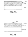
- a support 100 is formed, a first layer 102, based on a given material 103.
- the support 100 may be a substrate, or an upper layer of a stack of layers resting on a substrate.
- the support 100 may be for example a bulk substrate layer (commonly called “bulk” in the English terminology) based on Si, or substrate type semiconductor on insulation such as an SOI type substrate (SOI for "Silicon On Insulator” or silicon on insulator), or for example a layer of SiC on Si “bulk”, or for example an SiC substrate layer on Oxide (SiCOI).
- SOI SOI for "Silicon On Insulator” or silicon on insulator
- SiC substrate layer on Oxide SiC substrate layer on Oxide
- the given material 103 may be a material on which, or from which, graphene may be formed.
- the given material 103 is a material chosen to be compatible with growth of graphene sheets, and / or a material of which at least one thickness can be treated, for example by means of annealing, so as to be decomposed and transformed into a stack of several sheets of graphene.
- the given material 103 can be, for example, SiC or copper (Cu) or nickel (Ni) or iridium (Ir) or platinum (Pt) or ruthenium (Ru) or palladium (Pd).
- the first layer 102 may have a thickness for example between several nanometers and several tens of micrometers, for example between 100 nanometers and 20 micrometers ( Figure 1A ).
- a masking 105 is formed on the first layer 102, for example by deposition of a masking layer, for example based on Si x N y or on Si x O y resin or silicon oxide, and then etching this masking layer so as to define one or more masking patterns ( Figure 1B ).
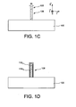
- the layer 102 of material 103 is then made of one or more elements of a component electromechanical, including at least one rod 108 based on the given material 103, this bar being intended to form a fixed member of the electromechanical component, and in particular to form an axis of rotation of this component.
- the bar 108 extends in a direction providing a non-zero angle, which may be 90 ° or close to 90 °, with the main plane of the support 100, (the main plane of the support 100 being defined as a plane passing through the latter and which is parallel to a plane [O; i ; j ] an orthogonal reference [O; i ; j ; k ] given on the figure 1C ).
- the bar 108 may be formed with a critical dimension dc, defined as the smallest dimension of the bar 108 and measured here in a plane parallel to the main plane of the support 100, may be between ten nanometers and several tens of micrometers, for example. example between 20 nanometers and 100 nanometers in the case where a nano-system is produced, or for example between 1 micrometer and 10 micrometers in the case where a micro-system is produced.
- the critical dimension dc can be adapted according to the intended application and the mass that the bar 108 may be intended to carry.
- the bar 108 may be made by anisotropic etching of the first layer 102 through the masking 105, for example using lithography with the aid of an electron beam followed by plasma etching. This etching can be performed until reaching the support 100.
- the masking 105 is then removed.
- the sheets 110 1 ... 110 n are formed in such a way that at least one first sheet 110 1 , and at least one second sheet 110 2 on the first sheet 110 1 , cover the bar 108 of given material 103.
- the number n of sheets formed can be for example between 2 and 10, or for example between 2 and several tens, or for example between 2 and several hundred.
- the sheets 110 1 ... 110 n of graphene may each consist of a monolayer of carbon atoms which may be of the order of 3 Angstroms thick or possibly several monolayers of carbon atoms.
- the sheets 110 1 ... 110 n of graphene can be formed by graphenization of a material deposited on the given material 103 or by graphenization of a thickness of the given material 103.
- the given material 103 can be, for example, SiC or copper (Cu) or nickel (Ni) or iridium (Ir) or platinum (Pt) or ruthenium (Ru) or palladium (Pd).
- the graphenization may be for example a graphenization of SiC made for example of the described in the document: "Ultrathin Epitaxial Graphite: 2D Electron Gas Properties and a Road Towards Graphene-based Nanoelectronics", Berger et al., American Chemical Society 2004 , or in the document: Forbeaux et al., Surf. Sci 442, 1999 , or in the document US 7,015,142 B1 .
- the sheets 110 1 ... 110 n of graphene can be formed on the layer of given material 103, by growth on the given material 103.
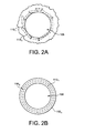
- the sheets 110 1 ... 110 n of graphene can respectively be in the form of a stack of continuous layers surrounding the bar 108 as represented for example on the Figure 2B , or in the form of a stack of distinct zones, distributed discontinuously around the bar 108 as shown for example on the Figure 2A (the Figures 2A and 2B giving a sectional view of the bar 108 in a sectional plane parallel to the main plane of the support 100 in the case given by way of example when the bar is of cylindrical shape).
- At least one first integral sheet of the bar 108 is formed which is bonded thereto, as well as at least one second sheet, which is disjoint from the first sheet or is not bonded to the first sheet, and is capable of be moved with respect to the bar 108 and the first leaflet.
- the first sheet is thus intended to form with the bar 108 a fixed member of the electromechanical component, while the second sheet is for forming a movable member portion of the electromechanical component.
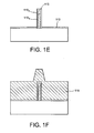
- a first layer of sacrificial material 113 is formed on the support 100 and on the bar 108.
- the material 113 may be formed by a non-conformal deposit, so that the material 113 does not cover the sides of the bar 108.
- the thickness of the deposited material 113 may be for example between several tens and several hundreds of nanometers.
- the sacrificial material 113 may be a material selected to be selectively etchable with the material 103 of the bar 108 and graphene sheets.
- the sacrificial material 113 may for example be SiO 2, in particular in the case where the bar 108 is based on SiC ( figure 1E ).
- the material 115 may be for example a metallic material.
- the material 115 may be deposited on the support 100 and on the element 108, in a thickness that may be for example between several tens and several hundreds of nanometers ( figure 1F ).
- a chemical mechanical polishing (CMP) step of the material 115 with a stop at the top of the bar 108, in particular up to the level of the top of the bar 108, can then be carried out by example in a case where the deposited material 115 exceeds the height of the bar 108.
- CMP chemical mechanical polishing
- a second layer of sacrificial material 117 resting on the top of the bar 108 and on the layer of material 115 is formed.
- the second layer of sacrificial material 117 can have a thickness that can be for example between several tens of nanometers and several hundreds of nanometers.
- the sacrificial material 117 may be selected to be selectively etchable with respect to the bar 108, graphene sheets, and the material 115 in which the movable member is to be formed.
- the sacrificial material 117 may be, for example, SiO 2 .
- An opening 119 is then formed in the layer of sacrificial material 117, so as to reveal the top of the bar 108.
- the opening 119 can be made using photolithography steps, and etching the second layer of sacrificial material 117 ( figure 1G ).
- a layer of material 125 is formed in which a protective element of the component, which may be in the form of a cover, is intended to be produced.
- the material 125 in which the cover will be formed may be chosen so that the materials 113 and 117 of the sacrificial layers may be etched selectively with respect to this material 125.
- the material 125 may be, for example, Si x N y , especially in the case where the sacrificial material layers 113 and 117 are based on SiO 2 .
- At least one pattern is then formed in the material layer 125 so as to define the cover. This can be achieved for example by photolithography steps, then anisotropic etching of the layer of material 125 ( figure 1H ).
- the movable element for example in the form of fins 121, 122, is defined in the layer of material 115.
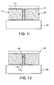
- the sacrificial layers 113 and 117 are removed, for example using steam HF.
- the movable member is thus released from the electromechanical component, for example in the form of fins 121, 122, of the support 100, and the cover 130 is thus separated from the fins 121 and 122 (FIG. Figure 1J ).
- Means for actuating the movable member for example electrostatic actuation means comprising one or more actuating electrodes, or electromagnetic actuating means can then be realized.
- an electromechanical component has been produced with a fixed member in the form of a bar 108 forming an axis of rotation, based on the material 103 covered with one or more first sheets ( s) of graphene bonded to the material 103 of the bar 108.
- the electromechanical component is also provided with a member movable in rotation around the bar 108.
- the movable member comprises one or more second graphene sheet (s) which are not bonded to the material 102 of the bar 108 and to the first sheets and which are capable of moving around the bar 108.
- the second sheet (s) of graphene are integral with the fins 121, 122 and intended to rotate around at least a bar portion 108.
- a cover 130 retaining is provided at the top of the bar 108, and may have for role , that of allowing to prevent detachment of the fins 121, 122 and a protective role.
- Some leaflets can be linked to each other, for example by Van de Waals type links.
- Van de Waals type links To allow to obtain a free movement of the second sheets with respect to the first sheets, one can break these links for example by actuating the movable member of the component.
- a setting in motion of the movable member can make it possible to break or eliminate the bonds between the graphene sheet (s) bound (s) to the bar 108 and the graphene sheet (s) of the movable member, which are integral with the fins.
- One can thus obtain a free rotation of the movable member around the bar forming the axis of rotation.
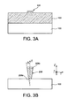
- the first layer 102, based on the given material 103 is formed ( figure 3A ), in which a rod 208 is formed based on the given material 103 intended to form an axis of rotation of the component.
- the bar 208 made is perpendicular to the main plane of the support 100, and has a flared shape with a base 208a resting on the support 100, less wide than its top 208b.
- the bar 208 may be formed with flanks forming an angle ⁇ , inclined relative to a normal not at the main plane of support 100.
- the bar 208 can be produced by etching the first layer 102 through a mask 105. This etching can be carried out until the support 100 is reached.
- the masking 105 is then removed ( figure 3B ). Then, the bar 208 can be given a rounded profile, for example by annealing under a hydrogen atmosphere at a temperature for example between 850 ° C and 900 ° C.
- the step of graphenization of the bar 208 is then carried out ( figure 3C ) or growth in which is formed on or from the bar 208, a stack of several sheets 110 1 ... 110 n of graphene, with at least one graphene sheet integral with the bar 208, and at least one second sheet disjoint from the first graphene sheet and movable relative to the first sheet.
- the bar 208 flared shape can be covered with graphene.
- the first layer of sacrificial material 113 is then formed on the support 100 and on the bar 208, for example by a deposit which is not in conformity, and which is designed so as to cover the the top of the bar 208 and the support 100, without covering the flanks of the bar 208 ( 3D figure ).
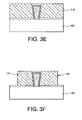
- the material 115 is then deposited around the bar 208 in which at least one component member of the component is intended to be formed ( figure 3E ). In the case where the material 115 covers the bar 208, a polishing step of the material 115 may be provided.
- the movable member element is formed, for example fins 121, 122 by etching the material 115 (FIG. figure 3F ).
- the sacrificial material 113 at the top of the bar 208 is then removed, as well as on the support 100, so as to release the fins 121, 122 of the support 100 (FIG. figure 3G ).
- a first layer is formed, based on a material 204, which may be chosen in particular so as to be easily patterned and which may make it possible to form a rigid structure, for example a semiconductor material such as Si ( Figure 4A ).
- the bar 208 is perpendicular to the main plane of the support 200, and comprises, as in the previous example, a flared shape with a base resting on the support 200, less wide than its top.
- the bar 208 may be produced by etching the first layer 204 through a mask 105, for example using a plasma HCl / Br 2 / O 2 or SF 6 / O 2 . Masking 105 is then removed.
- the bar 208 can then be rounded off, for example by annealing under a hydrogen atmosphere at an elevated temperature, for example between 850 ° C. and 900 ° C.
- a given material 209 selected to be compatible with growth of graphene or from which graphene can be formed is formed on the bar 208.
- the given material 209 is a material on which or from which one or more layers, or layers, of graphene can be formed.
- the given material 209 may be, for example, amorphous carbon.
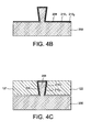
- a stack of several layers, or sheets 210 1 , 210 2 of graphene is formed, for example in a manner as described in the document: "Rapid Thermal annealing of amorphous hydrogeneted carbon films ", Alterovitz et al., meeting of the materials research society, 1987 , or the document Yaduda et al., Phys. Stat. Ground. 1986 , or the document “Electrical conductivity of prepared and annealed amorphous hydrogenated carbon films," Reyes-Mena et al., Journal of Vacuum Science Technology, May June 1990 ( Figure 4B ).
- the material 115 is then deposited around the bar 208 in which the movable member element, for example fins, is intended to be formed. Then, this element is formed, for example these fins 121, 122, by etching the material 115.
- the movable member element for example fins
- Such etching is performed in order to remove the zones of the given material 209 and graphene which cover the surface of the support 200, and to release the fins 121, 122 ( figure 4C ).
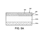
- a first layer 302 based on a given material 303 is first formed on a support 300, so that at least a portion of its thickness can be decomposed and converted into a plurality of graphene sheets. or chosen so that it can serve as growth support for graphene.
- the given material 303 may be, for example, monocrystalline or polycrystalline SiC.
- the first layer 302 may have a thickness for example between several nanometers and several hundred nanometers, for example between 10 and 500 nm.
- the support 300 may comprise an upper layer 301c of a substrate or a stack of layers resting on a substrate, on which the first layer 302 is made.
- the upper layer 301c is based on a material chosen so that the first layer 302 of given material 303 can be etched selectively against the upper layer 301c.
- the upper layer 301c may be based on a semiconductor material, for example such as Si.
- the upper layer 301c may have a thickness of, for example, between about ten nanometers and one hundred micrometers.
- the upper layer 301c rests on an intermediate layer 301b which can be insulating, for example based on SiO 2 , and of the order of a hundred nanometers thick.
- the upper layer 301c is preferably also provided so that it can be etched selectively with respect to the intermediate layer 301b.
- the intermediate layer 301b rests on a support layer 301a, and can be etched selectively with respect to the support layer 301a.
- This support layer 301a may be semiconductive, for example based on Si ( Figure 5A ).
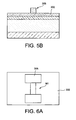
- Masking 305 for example resin or for example based on a metal such as aluminum to resist an etching step of the first layer 302, is then formed on the first layer 302.
- the masking 305 can have a pattern for example such as that M 1 given in Figure 6A having a zone of substantially rectangular shape connecting two rectangular zones of greater width ( Figures 5B and 6A ).
- a bar 308 is formed in the given material layer 303 for forming an axis of rotation of the electromechanical component.
- the bar 308 is produced by etching the first layer 302, for example by plasma etching such as RIE (RIE for "Reactive Ion Etching") or high density etching, for example using CHF 3 / O 2 , in in particular, the selective etching carried out is an etching of SiC with respect to Si.
- plasma etching such as RIE (RIE for "Reactive Ion Etching"
- high density etching for example using CHF 3 / O 2
- the selective etching carried out is an etching of SiC with respect to Si.
- the bar 308 formed extends in a direction parallel to the main plane of the support 300, that is to say a plane passing through the support 300 and parallel to a plane [O; i ; j ] an orthogonal reference [O; i ; j ; k ] defined on the Figures 5C and 6B .
- the bar 308 can be formed with a critical dimension dc for example between several tens of nanometers and several hundred nanometers, or between 10 nanometers and 10 micrometers.
- the critical dimension dc is defined as the smallest dimension of the bar 308 measured here in a direction parallel to the main plane of the support 300. This critical dimension can be adapted according to the intended application and the mass that the bar 108 can be intended to wear.
- one or more steps are performed to give the bar 308 a rounded profile.
- This can be achieved, for example, by means of an etching process, for example in hydrogen, and / or a heat treatment, for example by heating at a temperature of between 700 ° C. and 1200 ° C.
- a step of forming graphene is performed on the bar 308, in the form of a stack of several sheets 110 1 ... 110 n .
- a stack of n sheets 110 1 ... 110 n of graphene, with n for example between 2 and 100, of thickness between 0.6 and 40 nanometers can be achieved.
- At least two of the graphene sheets of the stack are separated, so that at least one sheet is secured to the bar and fixed and at least one second sheet is movable relative to the bar 308.
- a layer of material 315 is then formed around the bar 308 in which a component member 321 of the component is intended to be made.
- the material 315 can be for example a metallic material such as Al, TiN, or Ti, which is deposited for example by CVD (CVD for "Chemical vapor deposition") or PECVD (PECVD for "Plasma Enhanced Chemical vapor deposition ”) on the intermediate layer 301b support 300 ( Figure 5F and 6E ).
- the element 321 of the mobile component is formed.
- the material 315 is a metallic material
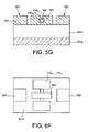
- electrodes 351, 352 for actuating the movable member may also be made in the material 315, at the same time as the element 321 ( Figure 5G and Figure 6F ). This can be done by photolithography, then etching the material 315, for example by plasma etching using a chlorinated element such as Cl 2 , BCl 3 , especially when the material 315 is aluminum.
- the element 321 is released, by etching the intermediate layer 301b through the patterns made in the material 315 and the upper layer 301b.
- This can be achieved by means of an isotropic etching, for example an etching with liquid HF or vapor HF.
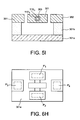
- the withdrawal can be realized so that portions P'1, P'2, (delimited by discontinuous lines on the Figures 5I and 6H ) of the intermediate layer 301b, are preserved under the portions P1 and P2 of the upper layer 301a, portions P'3, P'4 of the intermediate layer 301b, are preserved under the electrodes 351, 352, to ensure a mechanical strength of the stack.
- the removal of a portion of the intermediate layer 301b may be made so as to allow the element 321 of movable member to rotate around the bar 308.
- the bar 308 produced is attached to zones Z1, Z2 of anchor blocks which are formed from the same layer as this bar 308, in a single material, which gives the structure increased strength, especially at the ends of the bar 308.
- a masking layer is formed, for example based on Si x N y , ( Figure 7A ).
- a masking 405 is formed, for example using photolithography steps and etching is performed. ( Figure 7B ).
- a parallelepiped bar 408 is then formed in the layer 402, for example by anisotropic etching through the mask 405.
- a portion of the silicon layer 402 is thus removed, for example using a plasma.
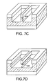
- the bar 408 formed is located in a cavity 411 and is attached to at least one anchor block formed in the same layer 402 of the same material 403 as the bar 408 ( Figure 7C ).
- a new etching is performed, for example an isotropic etching of the material 404 through the masking 405, so as to release the bar 408 of the support on which it rested, the bar being kept in suspension in the cavity 411 by said block.
- the isotropic etching may be carried out using TMAOH (Tetramethylammoniumhydroxide), which can confer a beveled shape to the bar 408 when the latter is based on Si ( Figure 7D ).
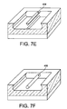
- the masking 405 is removed, for example using H 3 PO 4 .
- the bar 408 is given a rounded profile ( figure 7F ), for example by annealing under a hydrogen atmosphere at a temperature for example between 850 ° C and 900 ° C.
- a given material 409 is formed on which, or from which, graphene can be formed into several sheets 410 1 ... 410 n .
- the given material 409 may be, for example, amorphous carbon in the case where graphene is formed from material 409, or SiC.
- one of the stacked graphene leaflets 410 1 ... 410 n is formed , which will be separated so as to keep at least one graphene sheet secured to the bar 408, and at least one second sheet separated from the first graphene sheet, and capable of moving relative to the first sheet ( Figure 7G ).
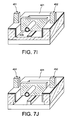
- a material 415 is then deposited around the bar 408, which may be metallic, and in which actuating electrodes 451, 452 are formed, as well as an element 421 intended to form a member movable in rotation around the bar 408 and to to be actuated by the electrodes 451, 452 ( figure 7H ).
- This step may be performed through a resin mask (not shown) which may have the same pattern as that of the masking 405 formed in a subsequent process step.
- a thickness of the layer on which the element 421 rests is then removed, for example by etching the silicon layer 404 ( figure 7J ).
- the thickness removed depends on the movement that the element 421 of the electromechanical component is intended to perform, and may be provided so that this element 421 can rotate all around the circumference or around the bar 408.
- Isotropic etching of the material 404 can then be performed so as to release the element 421 ( figure 7K ).
- a substrate 500 is formed, for example an Si-based bulk substrate, or a semiconductor-on-insulator type substrate such as an SOI (Silicon On Insulator) substrate. on insulator), or for example a layer of SiC on Si “bulk", or for example an SiC substrate layer on Oxide (SiCOI), a masking 505.
- SOI Silicon On Insulator
- SiC SiC substrate layer on Oxide
- This masking 505 may be made for example by deposition of a masking layer for example based on Si x N y or silicon resin or oxide Si x O y , then etching this masking layer so as to define one or more masking patterns ( figure 8A ).
- At least one bar 508 intended to form a fixed member of the electromechanical component that one wishes to make is formed, the bar 508 extending in a direction orthogonal to the main plane of the support 500.
- the bar 508 can be made by anisotropic etching of the support portions 500 which are not protected by the masking 505.
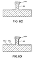
- an amorphous carbon layer 509 is deposited, which covers the support 500, the flanks of the bar 508 and the masking 505.
- the deposited amorphous carbon may be in conformity.
- This amorphous carbon layer 509 is then graphenized so as to form a stack of several layers, or leaflets 510 1 , ..., 510 n at least a first sheet 510 1 , and at least a second sheet 510 2 on the first sheet 510 1 , cover the bar 508 ( figure 8D ).
- At least a first sheet 510 1 is formed , which is bonded to or integral with the bar 508, and which is intended to form with this bar 508, a fixed member of the electromechanical component.
- at least one second free sheet 510 2 is also formed , which is disjoint from the first sheet 510 1 , and can be moved in rotation around the bar 508 and the first sheet 510 1 , the second sheet being intended to form part of movable member of the electromechanical component.
- a material 515 is formed, in which at least one moving element of the electromechanical component, for example in the form of of fins is intended to be realized.
- the material 515 may be for example a metallic material ( figure 8E ).
- a chemical mechanical polishing step (CMP) of the material 515 can then be performed.
- At least one moving member pattern of the structure for example fin patterns 521, 522 ( figure 8F ).
- This withdrawal may be carried out for example using a plasma, for example using an O 2 plasma (FIG. figure 8G ).
- An electromechanical component as described above can have many applications, and can be integrated in any micro-system or nano-system in which a rotational movement about an axis is implemented.
- the electromechanical component may allow for example to form a switch such as an electrical or optical switch.
- a switch with 2 stable positions whose position is implemented for example by means of Van der Waals forces, or for example by means of a magnetic force, can be provided.
- Electrostatic actuation of the fin 521 can be provided with one or more electrodes (not shown) positioned either laterally on either side of the fin, or below the fin. Magnetic actuation can also be provided. In this case, the presence of electrode is not necessary for a magnetic type actuation.
- Such a component provided with such a bar and such an arrangement of graphene sheets around the bar allows to implement a rotational movement in which the friction is decreased and the energy efficiency is increased.
- the graphene sheets make it possible to weaken the friction around the axis in rotation, and to make a rotation of the movable element around an axis without torsion, or with a negligible or very weak torsion of this element forming the rotation axis.
- Such a torsion would require the implementation of a restoring torque which would be counterbalanced via the application of various forces to maintain the switch in a stable position after actuation.
- maintaining the switch in a stable position can even be implemented using Van der Waals forces, for example by bonding between the fin and an area 599 on the support 500, which can be sufficient to hold the switch. in a given stable position without a force complementary, for example magnetic or electrostatic is necessary.
- the electromechanical system is more efficient and more robust.
Landscapes
- Engineering & Computer Science (AREA)
- Chemical & Material Sciences (AREA)
- Nanotechnology (AREA)
- Crystallography & Structural Chemistry (AREA)
- Condensed Matter Physics & Semiconductors (AREA)
- General Health & Medical Sciences (AREA)
- Materials Engineering (AREA)
- Physics & Mathematics (AREA)
- Composite Materials (AREA)
- Health & Medical Sciences (AREA)
- Life Sciences & Earth Sciences (AREA)
- General Physics & Mathematics (AREA)
- Molecular Biology (AREA)
- Computer Hardware Design (AREA)
- Microelectronics & Electronic Packaging (AREA)
- Mechanical Engineering (AREA)
- General Engineering & Computer Science (AREA)
- Micromachines (AREA)
- Carbon And Carbon Compounds (AREA)
Claims (9)
- Verfahren zur Herstellung eines elektromechanischen Mikrosystems mit wenigstens einem einen Stab umfassenden festen Organ und wenigstens einem beweglichen Organ, drehbar um wenigstens einen Teil des genannten Stabs, wobei das Verfahren die folgenden Schritte umfasst:a) Ausbildung - ausgehend von einer Schicht (102, 202, 302, 402) aus wenigstens einem auf einem Träger ruhenden bestimmten Material (103, 203, 303, 403) -, wenigstens eines Stabs (108, 208, 308, 408, 508), wobei das genannte bestimmte Material kompatibel ist mit einem Graphenblätter-Wachstum, oder wenigstens eine Dicke umfasst, die so behandelt werden kann, dass es zersetzt und umgewandelt wird in einen Stapel von mehreren Graphenblättern,b) Ausbildung, um den Stab herum, einer Vielzahl von Graphenblättern (1101, ..., 110n, 4101, ..., 410n), darunter wenigstens ein erstes Graphenblatt und wenigstens ein zweites Graphenblatt, getrennt von dem ersten Graphenblatt und beweglich in Bezug auf das erste Blatt, wobei das genannte zweite Graphenblatt dazu bestimmt ist, ein bewegliches Organteil des elektromechanischen Bauelements zu bilden.
- Verfahren nach Anspruch 1, bei dem, in Schritt a), wenigstens eine Ätzung der genannten Schicht (102, 202, 302, 402) des genannten bestimmten Materials (103, 203, 303, 403) durchgeführt wird, um den genannten Stab (108, 208, 308, 408) auszubilden.
- Verfahren nach einem der Ansprüche 1 oder 2, bei dem das bestimmte Material (103, 203, 303, 403) ein Material wie zum Beispiel SiC oder Kupfer (Cu) oder Nickel (Ni) oder Iridium (Ir) oder Platin (Pt) oder Ruthenium (Ru) oder Palladium (Pd) oder amorpher Kohlenstoff ist, auf dem ein Graphenwachstum realisiert werden kann oder von dem wenigstens eine Dicke zu Graphen zersetzt werden kann.
- Verfahren nach einem der Ansprüche 1 bis 3, wobei der Stab (208, 508) in Schritt a) so realisiert wird, dass er:- mit der Hauptebene des Trägers einen Nichtnullwinkel bildet,- zur Hauptebene des Trägers parallel ist.
- Verfahren nach Anspruch 4, bei dem der Stab (208, 508) in Schritt a) so realisiert wird, dass er mit der Hauptebene des Trägers einen Nichtnullwinkel bildet, wobei der Stab (508) dabei mittels Ätzung durch eine Maske von höherer kritischer Dimension als der des Stabs hindurch ausgebildet wird und die Blätter in Schritt b) so realisiert werden, dass sie den Stab und die Maske überdecken.
- Verfahren nach Anspruch 4, bei dem der Stab (208, 508) in Schritt a) so realisiert wird, dass er parallel ist zur Hauptebene des Trägers, wobei der Stab (308, 408) mit wenigstens einem Bereich eines Verankerungsblocks verbunden ist und der genannte Bereich zu der genannten Schicht aus bestimmtem Material gehört, in der der Stab in Schritt a) ausgebindet worden ist.
- Verfahren nach einem der Ansprüche 1 bis 6, außerdem umfassend: die Ausbildung wenigstens eines Elements (121, 122, 321, 421) des mit dem zweiten Graphenblatt verbundenen beweglichen Organs auf dem Stab.
- Verfahren nach einem der Ansprüche 1 bis 7, außerdem zwischen dem Schritt a) und dem Schritt b) umfassend: wenigstens einen Schritt zum Runden des Profils des Stabs.
- Verfahren nach einem der Ansprüche 1 bis 8, bei dem wenigstens eines der genannten eine kontinuierliche Schicht um den Stab herum bildenden Blätter und/oder die Blätter so geformt bzw. ausgebildet sind, dass der Umfang bzw. die Umrandung des Stabs mehrere Blätter umfasst.
Applications Claiming Priority (1)
| Application Number | Priority Date | Filing Date | Title |
|---|---|---|---|
| FR0956426A FR2950332B1 (fr) | 2009-09-18 | 2009-09-18 | Realisation d'un composant electromecanique pour un micro- ou nano- systeme dote d'un barreau formant un axe de rotation du composant et recouvert de graphene |
Publications (2)
| Publication Number | Publication Date |
|---|---|
| EP2298693A1 EP2298693A1 (de) | 2011-03-23 |
| EP2298693B1 true EP2298693B1 (de) | 2012-07-11 |
Family
ID=42224075
Family Applications (1)
| Application Number | Title | Priority Date | Filing Date |
|---|---|---|---|
| EP10177290A Not-in-force EP2298693B1 (de) | 2009-09-18 | 2010-09-17 | Verfahren zur Herstellung eines elektromechanischen Bauelementes für ein Mikro- oder Nano-System mit einem eine Rotationsachse des Bauelementes bildenden mit Graphen überzogenen Stab |
Country Status (4)
| Country | Link |
|---|---|
| US (1) | US8656584B2 (de) |
| EP (1) | EP2298693B1 (de) |
| JP (1) | JP2011098432A (de) |
| FR (1) | FR2950332B1 (de) |
Cited By (1)
| Publication number | Priority date | Publication date | Assignee | Title |
|---|---|---|---|---|
| CN112208052A (zh) * | 2020-09-29 | 2021-01-12 | 西安交通大学 | 一种基于磁性微粒导向的微型机器人及其制备方法 |
Families Citing this family (8)
| Publication number | Priority date | Publication date | Assignee | Title |
|---|---|---|---|---|
| FR2895835B1 (fr) | 2005-12-30 | 2008-05-09 | Commissariat Energie Atomique | Realisation sur une structure de canal a plusieurs branches d'une grille de transistor et de moyens pour isoler cette grille des regions de source et de drain |
| FR2946971B1 (fr) * | 2009-06-18 | 2011-07-15 | Commissariat Energie Atomique | Procede d'excitation d'un element mobile d'une microstructure |
| US11808214B2 (en) | 2021-05-24 | 2023-11-07 | General Electric Company | Midshaft rating for turbomachine engines |
| US12071978B2 (en) | 2021-05-24 | 2024-08-27 | General Electric Company | Midshaft rating for turbomachine engines |
| US11724813B2 (en) | 2021-05-24 | 2023-08-15 | General Electric Company | Midshaft rating for turbomachine engines |
| US12203377B2 (en) | 2021-05-24 | 2025-01-21 | General Electric Company | Midshaft rating for turbomachine engines |
| US11603801B2 (en) | 2021-05-24 | 2023-03-14 | General Electric Company | Midshaft rating for turbomachine engines |
| US12392307B2 (en) | 2023-03-24 | 2025-08-19 | General Electric Company | High-speed shaft rating for turbine engines |
Family Cites Families (12)
| Publication number | Priority date | Publication date | Assignee | Title |
|---|---|---|---|---|
| US4943750A (en) * | 1987-05-20 | 1990-07-24 | Massachusetts Institute Of Technology | Electrostatic micromotor |
| US6096149A (en) | 1997-04-21 | 2000-08-01 | Ford Global Technologies, Inc. | Method for fabricating adhesion-resistant micromachined devices |
| US6579833B1 (en) | 1999-09-01 | 2003-06-17 | The Board Of Trustees Of The University Of Illinois | Process for converting a metal carbide to carbon by etching in halogens |
| US6946851B2 (en) * | 2002-07-03 | 2005-09-20 | The Regents Of The University Of California | Carbon nanotube array based sensor |
| WO2005001895A2 (en) | 2003-06-12 | 2005-01-06 | Georgia Technology Research Corporation | Patterned thin film graphite devices and method for making same |
| US7053520B2 (en) * | 2003-07-18 | 2006-05-30 | The Regents Of The University Of California | Rotational actuator or motor based on carbon nanotubes |
| SG140447A1 (en) * | 2003-08-12 | 2008-03-28 | Sony Corp | Method of forming a micro-rotating device, and a micro-rotating device produced by the method |
| GB2422638A (en) * | 2005-01-27 | 2006-08-02 | Univ Lancaster | A rotational actuator |
| WO2006090400A2 (en) * | 2005-02-28 | 2006-08-31 | Bionnections Inc. | Method and structure for bio-mediated, self-assembled metal-filled nanotube devices and interconnects |
| WO2007119123A2 (en) * | 2005-08-26 | 2007-10-25 | Smoltek Ab | Interconnects and heat dissipators based on nanostructures |
| KR101303579B1 (ko) * | 2007-07-19 | 2013-09-09 | 삼성전자주식회사 | 전기기계적 스위치 및 그 제조방법 |
| WO2009102902A2 (en) * | 2008-02-14 | 2009-08-20 | The Charles Stark Draper Laboratory, Inc. | Rotary nanotube bearing structure and methods for manufacturing and using the same |
-
2009
- 2009-09-18 FR FR0956426A patent/FR2950332B1/fr not_active Expired - Fee Related
-
2010
- 2010-09-17 JP JP2010209718A patent/JP2011098432A/ja active Pending
- 2010-09-17 US US12/884,871 patent/US8656584B2/en not_active Expired - Fee Related
- 2010-09-17 EP EP10177290A patent/EP2298693B1/de not_active Not-in-force
Cited By (1)
| Publication number | Priority date | Publication date | Assignee | Title |
|---|---|---|---|---|
| CN112208052A (zh) * | 2020-09-29 | 2021-01-12 | 西安交通大学 | 一种基于磁性微粒导向的微型机器人及其制备方法 |
Also Published As
| Publication number | Publication date |
|---|---|
| FR2950332A1 (fr) | 2011-03-25 |
| FR2950332B1 (fr) | 2011-10-28 |
| JP2011098432A (ja) | 2011-05-19 |
| US8656584B2 (en) | 2014-02-25 |
| EP2298693A1 (de) | 2011-03-23 |
| US20110067985A1 (en) | 2011-03-24 |
Similar Documents
| Publication | Publication Date | Title |
|---|---|---|
| EP2298693B1 (de) | Verfahren zur Herstellung eines elektromechanischen Bauelementes für ein Mikro- oder Nano-System mit einem eine Rotationsachse des Bauelementes bildenden mit Graphen überzogenen Stab | |
| EP2299493B1 (de) | Herstellung von Silizium und Germanium Nanodrähten integrierte auf einem Substrat | |
| EP0766060B1 (de) | Herstellung eines mikromechanischen Teils mit mindestens einer Diamantspitze. | |
| EP2075222B1 (de) | Method of manufacturing mechanical components of MEMS or NEMS structures in monocrystalline silicon | |
| EP2617129B1 (de) | Vorrichtung mit freihängendem träger und piezoresistive vorrichtung zur verlagerungserkennung | |
| EP3339242B1 (de) | Mikroelektronische struktur mit kontrollmitteln für die viskose dämpfung | |
| EP2599746B1 (de) | Verfahren zur Herstellung einer Struktur mit mindestens einem aus mehreren Dicken bestehenden aktiven Teil | |
| EP2047509B1 (de) | Verfahren zur herstellung einer nanostruktur auf einem vorgeätzten substrat | |
| EP2599745B1 (de) | Verfahren zum Herstellen eines MEMS Bauteil mit bewegliche Teile unterschiedlicher Dicke | |
| EP1040492A1 (de) | Mikrostruktur mit einem verformbaren element durch einwirkung eines thermischen antriebes | |
| EP2808297B1 (de) | Verfahren zur Herstellung eines frei hängenden Teils einer mikro- und/oder nanoelektronischen Struktur in einem monolithischen Teil eines Substrats | |
| EP3424874B1 (de) | Sensorvorrichtung auf der basis von nanodrähten mit einer mobilen masse | |
| FR3059312A1 (fr) | Procede de realisation d’un dispositif electromecanique | |
| FR2875947A1 (fr) | Nouvelle structure pour microelectronique et microsysteme et procede de realisation | |
| FR3021965A1 (fr) | Procede de realisation ameliore d'elements suspendus d'epaisseurs differentes pour structure mems et nems | |
| EP2014611B1 (de) | MOS-Transistor mit frei hängendem Gate und nichtflüchtiger Funktionsweise mit piezoelektrische Aktivierung und Herstellungsverfahren desselben | |
| EP2138455B1 (de) | Verfahren zum Herstellen einer MEMS-Struktur mit einem beweglichen Element durch die Anwendung einer heterogenen Opferschicht | |
| FR3120622A1 (fr) | Commutateur MEMS à commande électrique et son procédé de réalisation | |
| EP2862836B1 (de) | Elektrochemisches Herstellungsverfahren mindestens einer porösen Zone einer mikro- und/oder nanoelektrischen Struktur | |
| EP3667309B1 (de) | Wärmeflusssensor mit heizdraht | |
| EP3828943A1 (de) | Mechanisches mikrosystem und entsprechendes herstellungsverfahren | |
| FR2912128A1 (fr) | Microsysteme d'actionnement et procede de fabrication associe | |
| FR2871790A1 (fr) | Microressort de grande amplitude | |
| EP3939935A1 (de) | Nanometrisches elektromechanisches stellglied und sein herstellungsverfahren | |
| FR2940799A1 (fr) | Architecture favorisant la formation de faisceaux denses de nanotubes ou de nanofils. |
Legal Events
| Date | Code | Title | Description |
|---|---|---|---|
| PUAI | Public reference made under article 153(3) epc to a published international application that has entered the european phase |
Free format text: ORIGINAL CODE: 0009012 |
|
| AK | Designated contracting states |
Kind code of ref document: A1 Designated state(s): AL AT BE BG CH CY CZ DE DK EE ES FI FR GB GR HR HU IE IS IT LI LT LU LV MC MK MT NL NO PL PT RO SE SI SK SM TR |
|
| AX | Request for extension of the european patent |
Extension state: BA ME RS |
|
| 17P | Request for examination filed |
Effective date: 20110418 |
|
| 17Q | First examination report despatched |
Effective date: 20110510 |
|
| GRAP | Despatch of communication of intention to grant a patent |
Free format text: ORIGINAL CODE: EPIDOSNIGR1 |
|
| RIC1 | Information provided on ipc code assigned before grant |
Ipc: B82Y 15/00 20110101ALI20120109BHEP Ipc: B82Y 30/00 20110101ALI20120109BHEP Ipc: B81B 5/00 20060101AFI20120109BHEP |
|
| GRAS | Grant fee paid |
Free format text: ORIGINAL CODE: EPIDOSNIGR3 |
|
| GRAA | (expected) grant |
Free format text: ORIGINAL CODE: 0009210 |
|
| AK | Designated contracting states |
Kind code of ref document: B1 Designated state(s): AL AT BE BG CH CY CZ DE DK EE ES FI FR GB GR HR HU IE IS IT LI LT LU LV MC MK MT NL NO PL PT RO SE SI SK SM TR |
|
| REG | Reference to a national code |
Ref country code: GB Ref legal event code: FG4D Free format text: NOT ENGLISH |
|
| REG | Reference to a national code |
Ref country code: CH Ref legal event code: EP |
|
| REG | Reference to a national code |
Ref country code: AT Ref legal event code: REF Ref document number: 566033 Country of ref document: AT Kind code of ref document: T Effective date: 20120715 |
|
| REG | Reference to a national code |
Ref country code: IE Ref legal event code: FG4D Free format text: LANGUAGE OF EP DOCUMENT: FRENCH |
|
| REG | Reference to a national code |
Ref country code: DE Ref legal event code: R096 Ref document number: 602010002163 Country of ref document: DE Effective date: 20120830 |
|
| REG | Reference to a national code |
Ref country code: NL Ref legal event code: VDEP Effective date: 20120711 |
|
| REG | Reference to a national code |
Ref country code: AT Ref legal event code: MK05 Ref document number: 566033 Country of ref document: AT Kind code of ref document: T Effective date: 20120711 |
|
| REG | Reference to a national code |
Ref country code: LT Ref legal event code: MG4D Effective date: 20120711 |
|
| PG25 | Lapsed in a contracting state [announced via postgrant information from national office to epo] |
Ref country code: AT Free format text: LAPSE BECAUSE OF FAILURE TO SUBMIT A TRANSLATION OF THE DESCRIPTION OR TO PAY THE FEE WITHIN THE PRESCRIBED TIME-LIMIT Effective date: 20120711 Ref country code: CY Free format text: LAPSE BECAUSE OF FAILURE TO SUBMIT A TRANSLATION OF THE DESCRIPTION OR TO PAY THE FEE WITHIN THE PRESCRIBED TIME-LIMIT Effective date: 20120711 Ref country code: FI Free format text: LAPSE BECAUSE OF FAILURE TO SUBMIT A TRANSLATION OF THE DESCRIPTION OR TO PAY THE FEE WITHIN THE PRESCRIBED TIME-LIMIT Effective date: 20120711 Ref country code: LT Free format text: LAPSE BECAUSE OF FAILURE TO SUBMIT A TRANSLATION OF THE DESCRIPTION OR TO PAY THE FEE WITHIN THE PRESCRIBED TIME-LIMIT Effective date: 20120711 Ref country code: NO Free format text: LAPSE BECAUSE OF FAILURE TO SUBMIT A TRANSLATION OF THE DESCRIPTION OR TO PAY THE FEE WITHIN THE PRESCRIBED TIME-LIMIT Effective date: 20121011 Ref country code: IS Free format text: LAPSE BECAUSE OF FAILURE TO SUBMIT A TRANSLATION OF THE DESCRIPTION OR TO PAY THE FEE WITHIN THE PRESCRIBED TIME-LIMIT Effective date: 20121111 Ref country code: HR Free format text: LAPSE BECAUSE OF FAILURE TO SUBMIT A TRANSLATION OF THE DESCRIPTION OR TO PAY THE FEE WITHIN THE PRESCRIBED TIME-LIMIT Effective date: 20120711 |
|
| PG25 | Lapsed in a contracting state [announced via postgrant information from national office to epo] |
Ref country code: PL Free format text: LAPSE BECAUSE OF FAILURE TO SUBMIT A TRANSLATION OF THE DESCRIPTION OR TO PAY THE FEE WITHIN THE PRESCRIBED TIME-LIMIT Effective date: 20120711 Ref country code: GR Free format text: LAPSE BECAUSE OF FAILURE TO SUBMIT A TRANSLATION OF THE DESCRIPTION OR TO PAY THE FEE WITHIN THE PRESCRIBED TIME-LIMIT Effective date: 20121012 Ref country code: SI Free format text: LAPSE BECAUSE OF FAILURE TO SUBMIT A TRANSLATION OF THE DESCRIPTION OR TO PAY THE FEE WITHIN THE PRESCRIBED TIME-LIMIT Effective date: 20120711 Ref country code: PT Free format text: LAPSE BECAUSE OF FAILURE TO SUBMIT A TRANSLATION OF THE DESCRIPTION OR TO PAY THE FEE WITHIN THE PRESCRIBED TIME-LIMIT Effective date: 20121112 Ref country code: SE Free format text: LAPSE BECAUSE OF FAILURE TO SUBMIT A TRANSLATION OF THE DESCRIPTION OR TO PAY THE FEE WITHIN THE PRESCRIBED TIME-LIMIT Effective date: 20120711 Ref country code: LV Free format text: LAPSE BECAUSE OF FAILURE TO SUBMIT A TRANSLATION OF THE DESCRIPTION OR TO PAY THE FEE WITHIN THE PRESCRIBED TIME-LIMIT Effective date: 20120711 |
|
| PG25 | Lapsed in a contracting state [announced via postgrant information from national office to epo] |
Ref country code: NL Free format text: LAPSE BECAUSE OF FAILURE TO SUBMIT A TRANSLATION OF THE DESCRIPTION OR TO PAY THE FEE WITHIN THE PRESCRIBED TIME-LIMIT Effective date: 20120711 |
|
| BERE | Be: lapsed |
Owner name: COMMISSARIAT A L'ENERGIE ATOMIQUE ET AUX ENERGIES Effective date: 20120930 |
|
| PG25 | Lapsed in a contracting state [announced via postgrant information from national office to epo] |
Ref country code: CZ Free format text: LAPSE BECAUSE OF FAILURE TO SUBMIT A TRANSLATION OF THE DESCRIPTION OR TO PAY THE FEE WITHIN THE PRESCRIBED TIME-LIMIT Effective date: 20120711 Ref country code: MC Free format text: LAPSE BECAUSE OF NON-PAYMENT OF DUE FEES Effective date: 20120930 Ref country code: ES Free format text: LAPSE BECAUSE OF FAILURE TO SUBMIT A TRANSLATION OF THE DESCRIPTION OR TO PAY THE FEE WITHIN THE PRESCRIBED TIME-LIMIT Effective date: 20121022 Ref country code: EE Free format text: LAPSE BECAUSE OF FAILURE TO SUBMIT A TRANSLATION OF THE DESCRIPTION OR TO PAY THE FEE WITHIN THE PRESCRIBED TIME-LIMIT Effective date: 20120711 Ref country code: DK Free format text: LAPSE BECAUSE OF FAILURE TO SUBMIT A TRANSLATION OF THE DESCRIPTION OR TO PAY THE FEE WITHIN THE PRESCRIBED TIME-LIMIT Effective date: 20120711 Ref country code: RO Free format text: LAPSE BECAUSE OF FAILURE TO SUBMIT A TRANSLATION OF THE DESCRIPTION OR TO PAY THE FEE WITHIN THE PRESCRIBED TIME-LIMIT Effective date: 20120711 |
|
| PLBE | No opposition filed within time limit |
Free format text: ORIGINAL CODE: 0009261 |
|
| STAA | Information on the status of an ep patent application or granted ep patent |
Free format text: STATUS: NO OPPOSITION FILED WITHIN TIME LIMIT |
|
| PG25 | Lapsed in a contracting state [announced via postgrant information from national office to epo] |
Ref country code: SK Free format text: LAPSE BECAUSE OF FAILURE TO SUBMIT A TRANSLATION OF THE DESCRIPTION OR TO PAY THE FEE WITHIN THE PRESCRIBED TIME-LIMIT Effective date: 20120711 Ref country code: IT Free format text: LAPSE BECAUSE OF FAILURE TO SUBMIT A TRANSLATION OF THE DESCRIPTION OR TO PAY THE FEE WITHIN THE PRESCRIBED TIME-LIMIT Effective date: 20120711 |
|
| 26N | No opposition filed |
Effective date: 20130412 |
|
| REG | Reference to a national code |
Ref country code: IE Ref legal event code: MM4A |
|
| PG25 | Lapsed in a contracting state [announced via postgrant information from national office to epo] |
Ref country code: BG Free format text: LAPSE BECAUSE OF FAILURE TO SUBMIT A TRANSLATION OF THE DESCRIPTION OR TO PAY THE FEE WITHIN THE PRESCRIBED TIME-LIMIT Effective date: 20121011 Ref country code: IE Free format text: LAPSE BECAUSE OF NON-PAYMENT OF DUE FEES Effective date: 20120917 Ref country code: BE Free format text: LAPSE BECAUSE OF NON-PAYMENT OF DUE FEES Effective date: 20120930 |
|
| REG | Reference to a national code |
Ref country code: DE Ref legal event code: R097 Ref document number: 602010002163 Country of ref document: DE Effective date: 20130412 |
|
| PG25 | Lapsed in a contracting state [announced via postgrant information from national office to epo] |
Ref country code: AL Free format text: LAPSE BECAUSE OF FAILURE TO SUBMIT A TRANSLATION OF THE DESCRIPTION OR TO PAY THE FEE WITHIN THE PRESCRIBED TIME-LIMIT Effective date: 20120711 Ref country code: MT Free format text: LAPSE BECAUSE OF FAILURE TO SUBMIT A TRANSLATION OF THE DESCRIPTION OR TO PAY THE FEE WITHIN THE PRESCRIBED TIME-LIMIT Effective date: 20120711 |
|
| PG25 | Lapsed in a contracting state [announced via postgrant information from national office to epo] |
Ref country code: TR Free format text: LAPSE BECAUSE OF FAILURE TO SUBMIT A TRANSLATION OF THE DESCRIPTION OR TO PAY THE FEE WITHIN THE PRESCRIBED TIME-LIMIT Effective date: 20120711 |
|
| PG25 | Lapsed in a contracting state [announced via postgrant information from national office to epo] |
Ref country code: SM Free format text: LAPSE BECAUSE OF FAILURE TO SUBMIT A TRANSLATION OF THE DESCRIPTION OR TO PAY THE FEE WITHIN THE PRESCRIBED TIME-LIMIT Effective date: 20120711 Ref country code: LU Free format text: LAPSE BECAUSE OF NON-PAYMENT OF DUE FEES Effective date: 20120917 |
|
| PG25 | Lapsed in a contracting state [announced via postgrant information from national office to epo] |
Ref country code: HU Free format text: LAPSE BECAUSE OF FAILURE TO SUBMIT A TRANSLATION OF THE DESCRIPTION OR TO PAY THE FEE WITHIN THE PRESCRIBED TIME-LIMIT Effective date: 20100917 |
|
| REG | Reference to a national code |
Ref country code: CH Ref legal event code: PL |
|
| PG25 | Lapsed in a contracting state [announced via postgrant information from national office to epo] |
Ref country code: MK Free format text: LAPSE BECAUSE OF FAILURE TO SUBMIT A TRANSLATION OF THE DESCRIPTION OR TO PAY THE FEE WITHIN THE PRESCRIBED TIME-LIMIT Effective date: 20120711 Ref country code: LI Free format text: LAPSE BECAUSE OF NON-PAYMENT OF DUE FEES Effective date: 20140930 Ref country code: CH Free format text: LAPSE BECAUSE OF NON-PAYMENT OF DUE FEES Effective date: 20140930 |
|
| REG | Reference to a national code |
Ref country code: FR Ref legal event code: PLFP Year of fee payment: 6 |
|
| PGFP | Annual fee paid to national office [announced via postgrant information from national office to epo] |
Ref country code: DE Payment date: 20150914 Year of fee payment: 6 Ref country code: GB Payment date: 20150921 Year of fee payment: 6 |
|
| PGFP | Annual fee paid to national office [announced via postgrant information from national office to epo] |
Ref country code: FR Payment date: 20150930 Year of fee payment: 6 |
|
| REG | Reference to a national code |
Ref country code: DE Ref legal event code: R119 Ref document number: 602010002163 Country of ref document: DE |
|
| GBPC | Gb: european patent ceased through non-payment of renewal fee |
Effective date: 20160917 |
|
| REG | Reference to a national code |
Ref country code: FR Ref legal event code: ST Effective date: 20170531 |
|
| PG25 | Lapsed in a contracting state [announced via postgrant information from national office to epo] |
Ref country code: FR Free format text: LAPSE BECAUSE OF NON-PAYMENT OF DUE FEES Effective date: 20160930 Ref country code: GB Free format text: LAPSE BECAUSE OF NON-PAYMENT OF DUE FEES Effective date: 20160917 Ref country code: DE Free format text: LAPSE BECAUSE OF NON-PAYMENT OF DUE FEES Effective date: 20170401 |