EP2299314A1 - Dispositif d affichage à cristaux liquides - Google Patents
Dispositif d affichage à cristaux liquides Download PDFInfo
- Publication number
- EP2299314A1 EP2299314A1 EP09770090A EP09770090A EP2299314A1 EP 2299314 A1 EP2299314 A1 EP 2299314A1 EP 09770090 A EP09770090 A EP 09770090A EP 09770090 A EP09770090 A EP 09770090A EP 2299314 A1 EP2299314 A1 EP 2299314A1
- Authority
- EP
- European Patent Office
- Prior art keywords
- liquid crystal
- divisional
- drive operation
- voltage
- application voltage
- Prior art date
- Legal status (The legal status is an assumption and is not a legal conclusion. Google has not performed a legal analysis and makes no representation as to the accuracy of the status listed.)
- Withdrawn
Links
Images




Classifications
-
- G—PHYSICS
- G09—EDUCATION; CRYPTOGRAPHY; DISPLAY; ADVERTISING; SEALS
- G09G—ARRANGEMENTS OR CIRCUITS FOR CONTROL OF INDICATING DEVICES USING STATIC MEANS TO PRESENT VARIABLE INFORMATION
- G09G3/00—Control arrangements or circuits, of interest only in connection with visual indicators other than cathode-ray tubes
- G09G3/20—Control arrangements or circuits, of interest only in connection with visual indicators other than cathode-ray tubes for presentation of an assembly of a number of characters, e.g. a page, by composing the assembly by combination of individual elements arranged in a matrix no fixed position being assigned to or needed to be assigned to the individual characters or partial characters
- G09G3/34—Control arrangements or circuits, of interest only in connection with visual indicators other than cathode-ray tubes for presentation of an assembly of a number of characters, e.g. a page, by composing the assembly by combination of individual elements arranged in a matrix no fixed position being assigned to or needed to be assigned to the individual characters or partial characters by control of light from an independent source
- G09G3/36—Control arrangements or circuits, of interest only in connection with visual indicators other than cathode-ray tubes for presentation of an assembly of a number of characters, e.g. a page, by composing the assembly by combination of individual elements arranged in a matrix no fixed position being assigned to or needed to be assigned to the individual characters or partial characters by control of light from an independent source using liquid crystals
- G09G3/3611—Control of matrices with row and column drivers
- G09G3/3648—Control of matrices with row and column drivers using an active matrix
-
- G—PHYSICS
- G09—EDUCATION; CRYPTOGRAPHY; DISPLAY; ADVERTISING; SEALS
- G09G—ARRANGEMENTS OR CIRCUITS FOR CONTROL OF INDICATING DEVICES USING STATIC MEANS TO PRESENT VARIABLE INFORMATION
- G09G2300/00—Aspects of the constitution of display devices
- G09G2300/04—Structural and physical details of display devices
- G09G2300/0439—Pixel structures
- G09G2300/0443—Pixel structures with several sub-pixels for the same colour in a pixel, not specifically used to display gradations
- G09G2300/0447—Pixel structures with several sub-pixels for the same colour in a pixel, not specifically used to display gradations for multi-domain technique to improve the viewing angle in a liquid crystal display, such as multi-vertical alignment [MVA]
-
- G—PHYSICS
- G09—EDUCATION; CRYPTOGRAPHY; DISPLAY; ADVERTISING; SEALS
- G09G—ARRANGEMENTS OR CIRCUITS FOR CONTROL OF INDICATING DEVICES USING STATIC MEANS TO PRESENT VARIABLE INFORMATION
- G09G2320/00—Control of display operating conditions
- G09G2320/02—Improving the quality of display appearance
- G09G2320/0252—Improving the response speed
-
- G—PHYSICS
- G09—EDUCATION; CRYPTOGRAPHY; DISPLAY; ADVERTISING; SEALS
- G09G—ARRANGEMENTS OR CIRCUITS FOR CONTROL OF INDICATING DEVICES USING STATIC MEANS TO PRESENT VARIABLE INFORMATION
- G09G2320/00—Control of display operating conditions
- G09G2320/02—Improving the quality of display appearance
- G09G2320/0271—Adjustment of the gradation levels within the range of the gradation scale, e.g. by redistribution or clipping
- G09G2320/0276—Adjustment of the gradation levels within the range of the gradation scale, e.g. by redistribution or clipping for the purpose of adaptation to the characteristics of a display device, i.e. gamma correction
-
- G—PHYSICS
- G09—EDUCATION; CRYPTOGRAPHY; DISPLAY; ADVERTISING; SEALS
- G09G—ARRANGEMENTS OR CIRCUITS FOR CONTROL OF INDICATING DEVICES USING STATIC MEANS TO PRESENT VARIABLE INFORMATION
- G09G2320/00—Control of display operating conditions
- G09G2320/02—Improving the quality of display appearance
- G09G2320/028—Improving the quality of display appearance by changing the viewing angle properties, e.g. widening the viewing angle, adapting the viewing angle to the view direction
-
- G—PHYSICS
- G09—EDUCATION; CRYPTOGRAPHY; DISPLAY; ADVERTISING; SEALS
- G09G—ARRANGEMENTS OR CIRCUITS FOR CONTROL OF INDICATING DEVICES USING STATIC MEANS TO PRESENT VARIABLE INFORMATION
- G09G2320/00—Control of display operating conditions
- G09G2320/06—Adjustment of display parameters
- G09G2320/0673—Adjustment of display parameters for control of gamma adjustment, e.g. selecting another gamma curve
-
- G—PHYSICS
- G09—EDUCATION; CRYPTOGRAPHY; DISPLAY; ADVERTISING; SEALS
- G09G—ARRANGEMENTS OR CIRCUITS FOR CONTROL OF INDICATING DEVICES USING STATIC MEANS TO PRESENT VARIABLE INFORMATION
- G09G2320/00—Control of display operating conditions
- G09G2320/06—Adjustment of display parameters
- G09G2320/068—Adjustment of display parameters for control of viewing angle adjustment
-
- G—PHYSICS
- G09—EDUCATION; CRYPTOGRAPHY; DISPLAY; ADVERTISING; SEALS
- G09G—ARRANGEMENTS OR CIRCUITS FOR CONTROL OF INDICATING DEVICES USING STATIC MEANS TO PRESENT VARIABLE INFORMATION
- G09G3/00—Control arrangements or circuits, of interest only in connection with visual indicators other than cathode-ray tubes
- G09G3/20—Control arrangements or circuits, of interest only in connection with visual indicators other than cathode-ray tubes for presentation of an assembly of a number of characters, e.g. a page, by composing the assembly by combination of individual elements arranged in a matrix no fixed position being assigned to or needed to be assigned to the individual characters or partial characters
- G09G3/34—Control arrangements or circuits, of interest only in connection with visual indicators other than cathode-ray tubes for presentation of an assembly of a number of characters, e.g. a page, by composing the assembly by combination of individual elements arranged in a matrix no fixed position being assigned to or needed to be assigned to the individual characters or partial characters by control of light from an independent source
- G09G3/36—Control arrangements or circuits, of interest only in connection with visual indicators other than cathode-ray tubes for presentation of an assembly of a number of characters, e.g. a page, by composing the assembly by combination of individual elements arranged in a matrix no fixed position being assigned to or needed to be assigned to the individual characters or partial characters by control of light from an independent source using liquid crystals
- G09G3/3607—Control arrangements or circuits, of interest only in connection with visual indicators other than cathode-ray tubes for presentation of an assembly of a number of characters, e.g. a page, by composing the assembly by combination of individual elements arranged in a matrix no fixed position being assigned to or needed to be assigned to the individual characters or partial characters by control of light from an independent source using liquid crystals for displaying colours or for displaying grey scales with a specific pixel layout, e.g. using sub-pixels
Definitions
- the present invention relates to a liquid crystal display device configured by a liquid crystal of a Vertical Alignment (VA) mode.
- VA Vertical Alignment
- liquid crystal display device adopting the VA (Vertical Alignment) mode using a vertically-aligned liquid crystal, for example.
- VA Vertical Alignment
- the liquid crystal molecules are each with the negative dielectric anisotropy, that is, the molecules have the properties in which the dielectric constant in the long-axis direction thereof is lower than that in the short-axis direction thereof, thereby realizing the viewing angle wider than that with the TN (Twisted Nematic) mode.
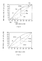
- FIG. 14 is a diagram showing the relationship between, in the liquid crystal display device using the VA-mode liquid crystal, the gray-scale (0 to 255 gray-scale levels) of a video signal and the luminance ratio (ratio to the luminance with the 255 gray-scale levels).
- the luminance characteristics show a large difference (show a variation toward a higher level of luminance) between when the display screen is viewed from the front direction (Ys(0°)) and when it is viewed from the direction (Ys(45°)).
- Such a phenomenon is referred to as "Shiratchake” namely, “Wash out” "Color Shift", and others, and is regarded as the major drawback of the liquid crystal display device using the VA-mode liquid crystal,
- FIG. 15 is a diagram showing an exemplary relationship between, in the multi-pixel structure, the gray-scale of a video signal and the display state of each of the sub pixels.
- the drawing shows that, in the process of a change of gray-scale level (an increase of luminance) from 0 (state of black display) to 255 (state of white display), first of all, a part (one sub pixel) of the pixel is increased in luminance, and then the remaining part (the other sub pixel) of the pixel is increased in luminance.
- a change of gray-scale level an increase of luminance
- 0 state of black display
- 255 state of white display
- the extent of the phenomenon of "wash out” is reduced with the luminance characteristics in the direction of 45° in the multi-pixel structure (Ym(45°)) compared with the luminance characteristics in the direction of 45° in the normal pixel structure (Ys(45°)).
- the extent of the phenomenon of "Wash out” is known to be reduced with the effects of halftone similarly to the case with the multi-pixel structure by dividing temporally a unit frame of display driving into a plurality of (e.g., two) sub frames, and also by representing any desired level of luminance with a combination of a sub frame(s) of high level of luminance and a sub frame(s) of low level of luminance.
- a halftone technique has the problem of easily causing the phenomenon as below, That is, first of all, as to a voltage to be applied to liquid crystal elements (liquid crystal application voltage), for transition thereof from low (e.g., gray-scale level of 0/gray-scale level of 255) to high (e.g., gray-scale level of 255/gray-scale level of 255), the halftone technique causes a steep increase of the voltage compared with the case of not using the technique. As a result, the luminance does not reach any desired value of voltage (value of luminance), thereby adversely affecting the response time of the liquid crystal.
- a voltage to be applied to liquid crystal elements liquid crystal application voltage
- Such a phenomenon is called “variation of azimuth angle of liquid crystal", and is resulted from the abrupt application of a high voltage to the liquid crystal that has been in the state of low voltage application. Due to the voltage application as such, the liquid crystal elements are once randomly oriented at various azimuth angles, and then are all aligned at any one desired azimuth angle.
- overdriving As another technique of improving the halftone response speed in the liquid crystal display device, overdriving is exemplified.
- This overdriving also causes a steep increase of the liquid crystal application voltage from low to high compared with the case of not using the halftone technique, and thus the response speed of the liquid crystal is indeed improved but a phenomenon called "rebounding" is easily occurred if the voltage of an original gray-scale value is applied to the liquid crystal after the completion of overdriving. This is because, due to the short-time application of a high voltage to the liquid crystal element by overdriving starting from the gray-scale level of 0 when the liquid crystal elements are in the vertical state, the liquid crystal elements in a part of the pixels are oriented differently but not those in the remaining part of the pixels.
- the viewing angle characteristics are indeed increased in terms of luminance but the phenomenon of variation of azimuth angle of liquid crystal or the phenomenon of rebounding is easily occurred. There thus have been problems of reducing the display characteristics of moving images, and degrading the display image quality.
- the present invention is proposed in consideration of the problems as above, and an object thereof is to provide a liquid crystal display device using a VA-mode liquid crystal with which the viewing angle characteristics are improved in terms of luminance, and at the same time, the display quality can be improved better than that with a previous liquid crystal display device.
- a first liquid crystal display device of the invention includes a plurality of pixels arranged in a matrix as a whole, and each provided with a liquid crystal element made of a liquid crystal of a vertical alignment (VA) mode; and a drive section driving the liquid crystal element of the pixels for display through applying a voltage based on an input video signal to the liquid crystal element, the drive section performing a divisional-drive operation through space-divisionally or time-divisionally dividing a display drive operation on each of the pixels into a plurality based on the input video signal.
- VA vertical alignment
- the divisional-drive operation is configured of a first divisional-drive operation group and a second divisional-drive operation group, the first divisional-drive operation group allowing a liquid crystal application voltage to be set into a higher-side voltage which is equal to or higher than an input application voltage, and a second divisional-drive operation group allowing the liquid crystal application voltage to be set into a lower-side voltage which is equal to or lower than the input application voltage, the liquid crystal application voltage representing a voltage to be applied to the liquid crystal elements, the input application voltage representing a voltage which corresponds to the input video signal.
- the drive section performs a divisional-drive operation belonging to the first divisional-drive operation group in such a manner that, the liquid crystal application voltage is higher than the input application voltage at least in an intermediate luminance range, whereas the liquid crystal application voltage is, in a highlight luminance range, equal to or higher than the input application voltage but shows a tendency to be lower compared to that in the intermediate luminance range.
- the drive section performs a divisional-drive operation belonging to the second divisional-drive operation group in such a manner that, the liquid crystal application voltage is lower than the input application voltage at least in the intermediate luminance range, whereas the liquid crystal application voltage is, in a lowermost luminance range, equal to or lower than the input application voltage but shows a tendency to be higher compared to that in the intermediate luminance range.
- the drive operation for execution to each of the pixels is space-divisionally or time-divisionally divided into a plurality to perform an operation of multiplex driving. Therefore, compared with the case of not performing such an operation of multiplex driving, any change (change from the case when the display screen is viewed in the front direction) to the gamma characteristics (characteristics showing the relationship between the gray-scale level of luminance of the video signal and the luminance) becomes less obvious when the display screen is viewed in the diagonal direction.
- the liquid crystal application voltage takes a higher-side voltage being equal to or higher than the input application voltage, and at the same time, shows a tendency to be lower compared to that in the intermediate luminance range. Therefore, compared with a previous operation of multiplex driving with which no such tendency to be low in voltage is observed in the highlight luminance range, the liquid crystal application voltage is prevented from abruptly increasing during voltage transition from low to high.
- the liquid crystal application voltage takes a lower-side voltage being equal to or lower than the input application voltage, and at the same time, shows a tendency to be higher compared to that in the intermediate luminance range. Therefore, compared with the previous operation of multiplex driving with which no such tendency to be high in voltage is observed in the lowermost luminance range, during overdriving, for example, the liquid crystal application voltage is prevented from abruptly increasing from low to high.
- a second liquid crystal display device of the invention includes the plurality of pixels described above, and a drive section driving the liquid crystal element of each of the pixels for display through applying a voltage based on an input video signal to the liquid crystal element, the drive section performing a divisional-drive operation through space-divisionally or time-divisionally dividing a display drive operation on each of the pixels into a plurality based on the input video signal.
- the divisional-drive operation is configured of the first divisional-drive operation group and the second divisional-drive operation group,
- the drive section performs a divisional-drive operation belonging to the first divisional-drive operation group in such a manner that, the liquid crystal application voltage is higher than the input application voltage at least in an intermediate luminance range, whereas the liquid crystal application voltage is, in a highlight luminance range, equal to or higher than the input application voltage but shows a tendency to be lower compared to that in the intermediate luminance range.
- the drive operation for execution to each of the pixels for display is spatially or temporally divided into a plurality to perform an operation of multiplex driving. Therefore, compared with the case of not performing such an operation of multiplex driving, any change to the gamma characteristics becomes less obvious when the display screen is viewed in the diagonal direction.
- the liquid crystal application voltage takes a higher-side voltage being equal to or higher than the input application voltage, and at the same time, shows a tendency to be lower compared to that in the intermediate luminance range. Therefore, compared with a previous operation of multiplex driving with which no such tendency to be low in voltage is observed in the highlight luminance range, the liquid crystal application voltage is prevented from abruptly increasing during voltage transition from low to high.
- a third liquid crystal display device of the invention includes the plurality of pixels described above, and a drive section driving the liquid crystal element of each of the pixels for display through applying a voltage based on an input video signal to the liquid crystal element, the drive section performing a divisional-drive operation through space-divisionally or time-divisionally dividing a display drive operation on each of the pixels into a plurality based on the input video signal.
- the divisional-drive operation is configured of the first divisional-drive operation group and the second divisional-drive operation group.
- the drive section performs a divisional-drive operation belonging to the second divisional-drive operation group in such a manner that, the liquid crystal application voltage is lower than the input application voltage at least in the intermediate luminance range, whereas the liquid crystal application voltage is, in a lowermost luminance range, equal to or lower than the input application voltage but shows a tendency to be higher compared to that in the intermediate luminance range,
- the drive operation for execution to each of the pixels for display is spatially or temporally divided into a plurality to perform an operation of multiplex driving. Therefore, compared with the case of not performing such an operation of multiplex driving, any change to the gamma characteristics becomes less obvious when the display screen is viewed in the diagonal direction.
- the liquid crystal application voltage takes a lower-side voltage being equal to or lower than the input application voltage, and at the same time, shows a tendency to be higher compared to that in the intermediate luminance range. Therefore, compared with a previous operation of multiplex driving with which no such tendency to be high in voltage is observed in the lowermost luminance range, for overdriving, for example, the liquid crystal application voltage is prevented from abruptly increasing from low to high.
- the drive operation for execution to each of the pixels for display is spatially or temporally divided into a plurality to perform an operation of multiplex driving. Therefore, compared with the case of not performing such an operation of multiplex driving, any change to the gamma characteristics becomes less obvious when the display screen is viewed in the diagonal direction so that the viewing angle characteristics can be improved in terms of luminance.
- the liquid crystal application voltage takes a higher-side voltage being equal to or higher than the input application voltage, and at the same time, shows a tendency to be lower compared to that in the intermediate luminance range. This thus can prevent the liquid crystal application voltage from abruptly increasing during voltage transition from low to high, thereby being able to prevent the occurrence of the variation of azimuth angle of the liquid crystal compared witch a previous operation of multiplex driving.
- the liquid crystal application voltage takes a lower-side voltage being equal to or higher than the input application voltage, and at the same time, shows a tendency to be lower compared to that in the intermediate luminance range. Accordingly, for overdriving, for example, this thus can prevent the liquid crystal application voltage from abruptly increasing from low to high, thereby being able to prevent the occurrence of the rebounding compared with the previous operation of multiplex driving. Therefore, in such a liquid crystal display device using a VA-mode liquid crystal, the viewing angle characteristics can be improved in terms of luminance, and at the same time, the display quality can be better than that in the previous liquid crystal display device.
- the drive operation for execution to each of the pixels for display is spatially or temporally divided into a plurality to perform an operation of multiplex driving. Therefore, compared with the case of not performing such an operation of multiplex driving, any change to the gamma characteristics becomes less obvious when the display screen is viewed in the diagonal direction so that the viewing angle characteristics can be improved in terms of luminance.
- the liquid crystal application voltage takes a higher-side voltage being equal to or higher than the input application voltage, and at the same time, shows a tendency to be lower compared to that in the intermediate luminance range.
- This thus can prevent the liquid crystal application voltage from abruptly increasing during voltage transition from low to high, thereby being able to prevent the occurrence of the variation of azimuth angle of the liquid crystal compared with a previous operation of multiplex driving. Therefore, in such a liquid crystal display device using a VA-mode liquid crystal, the viewing angle characteristics can be improved in terms of luminance, and at the same time, the display quality can be than that in the precious crystal display device.
- the drive operation for execution to each of the pixels for display is spatially or temporally divided into a plurality to perform an operation of multiplex driving. Therefore, compared with the case of not performing such an operation of multiplex driving, any change to the gamma characteristics becomes less obvious when the display screen is viewed in the diagonal direction so that the viewing angle characteristics can be improved in terms of luminance.
- the liquid crystal application voltage takes a lower-side voltage being equal to or lower than the input application voltage, and at the same time, shows a tendency to be higher compared to that in the intermediate luminance range. Accordingly, for overdriving, for example, this thus can prevent the liquid crystal application voltage from abruptly increasing from low to high, thereby being able to prevent the occurrence of the rebounding compared with the previous operation of multiplex driving. Therefore, in such a liquid crystal display device using a VA-mode liquid crystal, the viewing angle characteristics can be improved in terms of luminance, and at the same time, the display quality can be better than that in the previous liquid crystal display device.
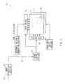
- FIG. 1 is a diagram showing the entire configuration of a liquid crystal display device (liquid crystal display device 1) in an embodiment of the invention.
- This liquid crystal display device 1 includes a liquid crystal display panel 2, a backlight section 3, an image processing section 41, a multi-pixel conversion section 43, a reference voltage generation section 45, a data driver 51, a gate driver 52, a timing control section 61, and a backlight control section 63.
- the backlight suction 3 is a light source from which a light is directed so the liquid crystal display panel 2, and is configured by including a CCFL (Cold Cathode FluorescentLamp), an LED (Light EmittingDiode), and others.
- CCFL Cold Cathode FluorescentLamp
- LED Light EmittingDiode
- the liquid crystal display panel 2 modulates the light coming from the backlight section 3 based on a drive voltage provided by the data driver 51 so that the resulting video display is made based on a video signal Din
- the liquid crystal display panel 2 includes a plurality of pixels 20 arranged in a matrix as a whole.
- the pixels 20 are those each corresponding to any one of R (Red), G and B (Blue) (pixels each emit a display light of R, G, or B corresponding to the color of a color filter for R, G, or B provided thereto (not shown)).
- the pixels 20 are each formed therein with a pixel circuit including two sub pixels (sub pixels 20A and 20B that will be described later). The configuration of such pixel circuits will be described later in detail ( FIGS. 2 and 3 ).
- the image processing section 41 generates a video signal D1 being an RGB signal by performing predetermined image processing with respect to a video signal Din coming from the outside.
- the multi-pixel conversion section 43 converts, by using a lookup table (LUT) that will be described later, the video signal D1 coming from the image processing section 41 into two video signals D2a and D2b for use respectively by the sub pixels (performs multi-pixel conversion), and supplies the resulting video signals D2a and D2b to the timing control section 61.
- This LUT provides the correlation between the video signal D1 and the video signals respectively corresponding to the sub pixels in terms of gray-scale level of luminance. Such a correlation is provided on the basis of a video signal of the pixel corresponding to any one of R, G, and B.
- the LUT will be described in more detail later ( FIG. 4 ).
- the reference voltage generation section 45 supplies a reference voltage Vref to the data driver 51 for use during D/A (Digital/Analog) conversion that will be described later.
- this reference voltage Vref covers a range of reference voltages from black voltage (voltage with the gray-scale level of 0 of luminance that will be described later) to white voltage (e.g., voltage with the gray-scale level of 255 of luminance that will be described later).
- black voltage voltage with the gray-scale level of 0 of luminance that will be described later
- white voltage e.g., voltage with the gray-scale level of 255 of luminance that will be described later.
- such a reference voltage Vref is shared by the pixels each corresponding to any one of R, G, and B. Note here that this reference voltage generation section 45 is in the resistor tree structure or others in which a plurality of resistors are connected in series, for example.
- the gate driver 52 line-sequentially drives the pixels 20 in the liquid crystal display panel 2 along scan lines that are not shown (gate lines G that will be described later) in accordance with timing control applied by the timing control section 61.
- the data driver 51 supplies a drive voltage to each of the pixels 20 (more in detail, to each of the sub pixels in each of the pixels 20) of the liquid crystal display panel 2 based on the video signals D2a and D2b coming from the timing control section 61.
- this data driver 51 is configured so as to generate video signals each being an analog signal (drive voltage described above). The resulting video signals are output to each of the pixels 20.
- the backlight drive section 62 controls the illumination operation of the backlight section 3.
- the timing control section 61 controls the drive timing of the driver 52 and that of the data driver 51, and supplies the video signals D2a and D2b to the data driver 51.
- FIG. 2 shows an exemplary circuit configuration of the pixel circuit in the pixel 20.
- FIG. 3 shows an exemplary configuration in a planar view of a pixel electrode in a liquid crystal element in the pixel circuit.
- the pixel 20 is configured by the two sub pixels 20A and 20B, and is in the multi-pixel structure.
- the sub pixel 20A includes a liquid crystal element 22A being a main capacitor, an auxiliary capacitor 23A, and a thin film transistor (TFT) element 21A.
- the sub pixel 20B includes a liquid crystal element 22B being a main capacitor, an auxiliary capacitor 23B, and a TFT element 21B.
- the pixel 20 is connected with a gate line G, two data lines DA and DB, and an auxiliary capacity line Cs.
- the gate line G is for line-sequentially selecting a pixel as a drive target, and the two data lines DA and DB are for supplying the drive voltage (drive voltage provided by the data driver 51) to each of the sub pixels 20A and 20B in the pixel being the drive target.
- the auxiliary capacity line Cs is a bus line for supplying a predetermined reference two the opposing electrode of the auxiliary capacitors 23A and 23B.
- the liquid crystal element 22A as a display element that operates for display (emits a display light) in accordance the drive voltage, which is provided to one end thereof the data line DA via the TFT element 21A.
- the liquid crystal element 22B as a display element that operates for display (emits a display light) in accordance with the drive voltage, which is provided to one end thereof from the data line DB via the TFT element 21B.
- These liquid crystal elements 22A and 22B are each configured to include a liquid crystal layer (not shown) made of a VA-mode liquid crystal, and a pair of electrodes (not shown) sandwiching this liquid crystal layer therebetween.
- the side of one of (one end of) these electrodes in pair (the side of reference numerals P1A and P1B in FIG. 2 ) is connected with the source of each of the TFT elements 21A and 21B, and with one end of each of the auxiliary capacitors 23A and 23B. The other side (the other end) thereof is grounded.
- the electrode on one side of the electrodes in pair (the side of reference numerals P1A and P1B in FIG. 2 ) is a flat-shaped pixel electrode 220 as shown in FIG. 3 , for example, and is configured by a pixel electrode on the side of the sub pixel 20A, and a pixel electrode on the side of the sub pixel 20B (a combination of 20B-1 and 20B-2).
- the auxiliary capacitors 23A and 23B are capacitors respectively for stabilizing the liquid crystal elements 22A and 22B in terms of their accumulated charge.
- One end of the auxiliary capacitor 23A (one of the electrodes) is connected to one end of the liquid crystal element 22A and to the source of the TFT element 21A, and the remaining end (opposing electrode) is connected to the auxiliary capacity line Cs.
- One end of the auxiliary capacitor 23B (one of the electrodes) is connected to one end of the liquid crystal element 22B and to the source of the TFT element 21B, and the remaining end (opposing electrode) is connected to the auxiliary capacity line Cs.
- the TFT element 21A is configured by a MOS-FET (Metal OxideSemiconductor-Field Transistor).
- MOS-FET Metal OxideSemiconductor-Field Transistor
- the gate is connected to the gate line G
- the source is connected to one end of the liquid crystal element 22A and to one end of the auxiliary capacitor 23A
- the drain is connected to the data line DA.
- This TFT element 21A as a switching for supplying a drive voltage (drive voltage based on the video signal D2a) for use by the sub pixel 20A to one end of the liquid crystal element 22A and to one end of the auxiliary capacitor 23A.
- the TFT element 21A is provided for selectively the continuity the data line DA and one end of the liquid crystal element 22A or between the data line DA and one end of the auxiliary capacitor 23A.
- the FTF element 21B is similarly configured by a MOS-FET, and therein, the gate is connected to the gate line G, the source is connected to one end of the liquid crystal element 22B and to one end of the auxiliary capacitor 23B, and the drain is connected to the data line DB.
- This TFT element 21B serves as a switching element for supplying a drive voltage (drive voltage based on the video signal D2b) for use by the sub pixel 20B to one end of the liquid crystal element 22B and to one end of the auxiliary capacitor 23B.
- the TFT element 21B is provided for selectively establishing the continuity between the data line DB and one end of the liquid crystal element 22B or between the data line DB and one end of the auxiliary capacitor 23B.
- the grays-scale level of luminance is set to fall within a range from 0/255 (state of black display) to 255/255 (state of white display).
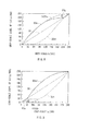
- Such an LUT is provided for use to divide the gray-scale level of luminance of the video signal D1 provided to the multi-pixel conversion section 43 as indicated by arrows P2a and P2b in FIG. 4 , for example.
- the division results are the gray-scale level of luminance of the video signal D2a for use by the sub pixel 20A, and the gray-scale level of luminance of the video signal D2b for use by the sub pixel 20B.
- the LUT is used for, based on the video signal D1, spatially dividing the drive operation to each of the pixels 20 for display into two to perform an operation of multiplex driving to each of the sub pixels 20A and 20B.
- such an operation of multiplex driving is a combination of a first operation of multiplex driving (operation of multiplex driving with respect to the sub pixel 20A) and a second operation of multiplex driving (operation of multiplex driving with respect to the sub pixel 208).
- the operation of multiplex driving is performed so that the liquid crystal application voltage to be applied to the liquid crystal element 22A takes a higher-side voltage being equal to or higher than an input application voltage corresponding to the video signal D1.
- the operation of multiplex driving is performed so that the liquid crystal application voltage to be applied to the liquid crystal element 22B takes a lower-side voltage being equal to or lower than the input application voltage described above.
- the liquid crystal application voltage to be applied to the liquid crystal element 22A is higher than the input application voltage corresponding to the video signal D1.
- the liquid crystal application voltage to be applied to the liquid crystal element 22A takes a higher-side voltage being equal to or higher than the input application voltage corresponding to the video signal D1, and at the same time, shows a tendency to be lower compared to that in the intermediate luminance range.
- the liquid crystal application voltage to be applied to the liquid crystal element 22A in such a highlight luminance range is set to be equal to or higher than the input application voltage corresponding to the video signal D1, and to be equal to or lower than the voltage with which the phenomenon of "variation of azimuth angle of liquid crystal" generally occurs.
- the liquid crystal application voltage to be applied to the liquid crystal element 22B is lower than the input application voltage corresponding to the video signal D1. Also as indicated by an arrow P3b in FIG. 4 , for example, in a lowermost luminance range, the liquid crystal application voltage to be applied to the liquid crystal element 22B takes a lower-side voltage being equal to or lower the input application voltage corresponding to the video signal D1, and at the same time, shows a two be higher than that in the intermediate luminance range.
- the liquid crystal application voltage to be applied to the liquid crystal element, 22B is set to a higher-side voltage which is equal to or higher than a minimum value of the voltage corresponding to the minimum gray-scale level of luminance (other than then gray-scale level of 0 in the video signal D1, the voltage is set so as not to be in the gray-scale level of 0 in the signal D2b).
- the components of the multi-pixel conversion section 43, the timing control section 61, the reference voltage generation section 45, the data driver 51, and the drive 52 are a specific example of a "drive section" in the invention.
- the LUT of FIG. 4 is a specific example of a "first LUST" in the invention.
- the sub pixel 20A is a specific example of a "first sub pixel group” in the invention, and the sub pixel 20B is a specific example of the "second sub pixel group” in the invention.
- the video signal Din coming from the outside is subjected to image processing by the image processing section 41, and the generation result is the video signal D1 for use by each of the pixels 20.
- This video signal D1 is provided to the multi-pixel conversion section 43.
- the video signal D1 provided as such is converted into the two video signals D2a and D2b for respective use by the sub pixels 20A and 20B (multi-pixel conversion).
- These two video signals D2a and D2b are each provided to the data driver 51 via the timing control section 61.
- the video signals D2a and D2b are subjected to D/A conversion using the reference voltage Vref provided by the reference voltage generation 45 so that two video signals each being an analog signal are generated.
- the pixels 20 are each driven for display by the drive voltage coming from the gate driver 52 and the data driver 51 for use by the sub pixels 20A and 20B in of the pixels 20.
- the TFT element 21A is turned ON/OFF and the TFT element 21B is turned OFF/ON, and the continuity is selectively established between the data lines DA and DB and the liquid crystal elements 22A and 22B or between the data lines DA and DB and the auxiliary capacitors 23A and 23B.
- the drive voltage based on the two video signals coming from the data driver 51 is provided to the liquid crystal elements 22A and 22B, and to the auxiliary capacitors 23A and 23B so that the pixels are driven for display.
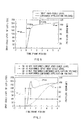
- FIGs. 5 to 7 are diagrams for illustrating an LUT in a previous liquid crystal display device in the comparison example, and problems with the use of the LUT.
- the drive operation to each of the pixels 20 is spatially divided into two based on the video signal D1 so that the resulting operation of multiplex driving is performed (refer to the arrows P2a and P2b in FIG. 4 ).
- each of the pixels 20 is a combination of the two sub pixels 20A and 20B, and also based on video signals D3a and D3b being the results of multi-pixel conversion to the video signal D1 (not shown; two video signals each being an analog signal coming from the data driver 51), the operation of multiplex driving is performed to each of the sub pixels 20A and 20B after the operation of driving the pixels 20 for display is spatially divided into two.
- any change (change from the case when the display screen is viewed in the front direction) to the gamma characteristics (characteristics showing the relationship the gray-scale level of luminance of the video signal D1 and the luminance) becomes less obvious the display screen is viewed in the diagonal direction (e.g., in the direction of 45°).
- the luminance characteristics Ym(45°C) in FIG. 14 for example, the viewing angle characteristics are improved in terms of luminance compared with the case of not performing the operation of multiplex driving in the multi-pixel structure (e.g., the luminance characteristics Ys(45°) in FIG. 14 ).
- the operation of multiplex driving in the multi-pixel structure is similarly performed (e.g., refer to arrows P102a and P102b in FIG. 5 ).
- the viewing angle characteristics are improved in terms of luminance.
- the operation of multiplex driving in the multi-pixel structure is performed using such an LUT as shown in FIG. 5 as an alternative to the LUT in the embodiment of FIG. 4 .
- this LUT for the operation in the operation of multiplex driving with respect to the sub pixel 20A (corresponding to a video signal D102a in FIG.
- the sub pixel 20A being in the much lower gray-scale level is a target for application of a high voltage compared with the case of not using the halftone technique, This is the reason why the time is adversely affected more often with a larger number of gray-scale levels by the "variation of azimuth angle of liquid crystal".
- the gray-scale level of 0 is in need more often than the case of not using the halftone technique. This thus requires a steep increase of the liquid crystal application voltage from low to high.
- the response speed of the liquid crystal is indeed improved by such overdriving but as indicated by a reference numeral P104 in FIG. 7 , for example, the "phenomenon of rebounding" is easily occurred if the voltage of an original gray-scale value is applied to the liquid crystal elements after the completion of overdriving.
- the liquid crystal application voltage to be applied to the liquid crystal element 22A takes a higher-side voltage being equal to or higher than the input application voltage corresponding to the video signal D1, and at the same time, shows a tendency to be lower compared to that in an intermediate luminance range.
- the liquid crystal application voltage to be applied to the liquid crystal element 22A in such a region with the high level of luminance is set to be equal to or higher the input application voltage corresponding to the video signal D1, and to be equal to or lower than the voltage with which the phenomenon of "variation of azimuth angle of liquid crystal" generally occurs.
- the liquid crystal application voltage is prevented from abruptly increasing during voltage transition from low to high.
- the liquid crystal application voltage to be applied to the liquid crystal element 22B takes a lower-side voltage being equal to or lower than the input application voltage corresponding to the video signal D1, and at the same time, shows a tendency to be higher compared to that in an intermediate luminance range.
- the liquid crystal application voltage to be applied to the liquid crystal element 22B is set to a higher-side voltage which is equal to or higher than a minimum value of the voltage corresponding to the minimum gray-scale level of luminance (other than the gray-scale level of 0 in the video signal D1, the voltage is set so as not to be in the gray-scale level of 0 in the video signal D2b).
- the liquid crystal application voltage is prevented from abruptly increasing during voltage transition from low to high. This accordingly reduces the number of gray-scale levels causing the "phenomenon of rebounding" (e.g., reduction from 64 to 20 gray-scale levels).
- a tendency to be low in voltage is conversely observed in the lowermost luminance range not to cause any change to the gamma characteristics compared with the case with the video signal D1.
- the drive operation for execution to each of the pixels 20 for display is spatially divided into two so that the resulting operation of multiplex driving is performed, Accordingly, compared with the of not performing such an operation of multiplex driving, any change to the gamma characteristics becomes less obvious when the display screen is viewed in the diagonal direction. This favorably leads to the better viewing angle characteristics in terms of luminance.
- the liquid crystal application voltage to be applied to the liquid crystal element 22A takes a higher-side voltage being equal to or higher than the input application voltage corresponding to the video signal D1, and at the same time, shows a tendency to be lower compared to that in an intermediate luminance range. This accordingly prevents the liquid crystal application voltage from abruptly increasing during voltage transition from low to high, thereby preventing the variation of azimuth angle of the liquid crystal compared with the previous operation of multiplex driving.
- the liquid crystal application voltage to be applied to the liquid crystal element 22B takes a lower-side voltage being equal to or lower than the input application voltage corresponding to the video signal D1, and at the same time, shows a tendency to be higher compared to that in an intermediate luminance range. Therefore, for overdriving, this accordingly prevents the liquid crystal application voltage from abruptly increasing from low to high, thereby preventing the occurrence of the phenomenon of rebounding compared with the previous operation of multiplex driving. Accordingly, in the liquid crystal display device using a VA-mode liquid crystal, the viewing angle characteristics can be improved in terms of luminance, and at the same time, the display image quality can be better than that in the previous liquid crystal display device.
- the pixels 20 each configured by the two sub pixels 20A and 20B and based on the video signals D3a and D3b being the results of the multi-pixel conversion executed to the video signal D1, the drive operation for execution to each of the pixels 20 for display being spatially divided into two to perform the operation of multiplex driving separately to each of the sub pixels 20A and 20B.
- the drive operation for execution to each of the pixels 20 for display can be spatially divided into two to perform the operation of multiplex driving separately to each of the sub pixels 20A and 20B.
- the liquid crystal application voltage to be applied to the liquid crystal element 228 is set so as to take a value on the higher-voltage side than a minimum value of the voltage corresponding to the minimum gray-scale level of luminance (other than the gray-scale level of 0 in the video signal D1, the voltage is set so as not to be in the gray-scale level of 0 in the video signal D2b). This accordingly prevents the occurrence of the phenomenon of rebounding during the overdriving.
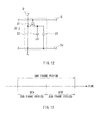
- the multi-pixel configuration in which of the pixels 20 is with a gate line G and two data lines DA and DB as the pixel 20 and the sub pixels 20A and 20B shown in FIG. 2 .
- the invention is surely applicable also to such a multi-pixel configuration in which each of the pixels 20-1 is connected with two gate lines GA and GB and a data line D.
- a pixel 20-1 for example, provided are two sub frame periods being the results of dividing a unit frame for display driving (a frame period) into two along a time axis, and the sub pixels 20A and 20B are driven in accordance with a selection signal provided within each of the sub frame periods over the gate lines GA and GB, and in accordance with a drive voltage provided by the data driver 51.
- the reference voltage for use to D/A-convert the video signal D1 coming from the image processing section 41 into the video signals D3a and D3b (not shown) in the data driver 51 may be set so as to vary between the sub pixels 20A and 20B (a reference voltage VrefA corresponding to the sub pixel 20A is different from a reference voltage VrefB corresponding to the sub pixel 20B).
- an operation to drive the pixels 20 for display may be spatially divided into two for performing an operation of multiplex driving separately to the sub pixels 20A and 20B. If this is the configuration, the effects similar to those in the above embodiments can be favorably achieved. Also in this case, the multi-pixel configuration as shown in FIG. 10 is applicable.
- each of the pixels 20 is configured by the two sub pixels 20A and 20B, and an operation to drive the pixels 20 for display is spatially divided into two for performing an operation of multiplex driving separately to the sub pixels 20A and 20B.
- a pixel 20-2 in the normal single a shown in Fig. 12 e.g., pixel including one liquid crystal element 22, one auxiliary capacitor 23, and one TFT element 21 with a connection established with a gate line G and a data line D
- the effects of halftone may be derived similarly to the case with the multi-pixel structure by temporally dividing a unit frame for display driving (a frame period) into two sub frame periods SFA and SFB, and by representing any desired level of luminance using a combination of a sub frame(s) SFA of high level of luminance and a sub frame(s) SFB of low level of luminance.
- a unit frame for display driving (a frame period) into two sub frame periods SFA and SFB
- any desired level of luminance using a combination of a sub frame(s) SFA of high level of luminance and a sub frame(s) SFB of low level of luminance.
- an operation to drive the pixels 20-2 for display is temporally divided into two for performing an operation of multiplex driving separately to the sub frame periods SFA and SFB.
- the operation of multiplex driving at this time is a combination of a first operation of multiplex driving (operation of multiplex driving with respect to the sub frame period SFA) and a second operation of multiplex driving (operation of multiplex driving with respect to the sub frame period SFB).
- the first operation of multiplex driving the operation of multiplex driving is performed so that the liquid crystal application voltage to be applied to the liquid crystal element 22 takes a higher-side voltage being equal to or higher than the input application voltage corresponding to the video signal D1.
- the operation of multiplex driving is performed so that the liquid crystal application voltage to be applied to the liquid crystal element 22 takes a lower-side voltage being equal to or lower than the input application voltage described above.
- an LUT providing the correlation between the video signal D1 and the video signals respectively corresponding to the sub frame periods SFA and SFB may be used.
- the reference voltage for use to D/A-convert the video signal D1 may be set so as to vary between the sub frame periods SFA and SFB. If these are the configurations, the effects similar to those in the above embodiment can be successfully achieved.
- the number of the sub pixels in each of the pixels 20 and the number of the sub frame periods in a frame period are both surely not restrictive to two as exemplified above, and both may be three or more.
Landscapes
- Engineering & Computer Science (AREA)
- Chemical & Material Sciences (AREA)
- Crystallography & Structural Chemistry (AREA)
- Physics & Mathematics (AREA)
- Computer Hardware Design (AREA)
- General Physics & Mathematics (AREA)
- Theoretical Computer Science (AREA)
- Control Of Indicators Other Than Cathode Ray Tubes (AREA)
- Liquid Crystal (AREA)
- Liquid Crystal Display Device Control (AREA)
Applications Claiming Priority (2)
| Application Number | Priority Date | Filing Date | Title |
|---|---|---|---|
| JP2008167535A JP4840412B2 (ja) | 2008-06-26 | 2008-06-26 | 液晶表示装置 |
| PCT/JP2009/061184 WO2009157380A1 (fr) | 2008-06-26 | 2009-06-19 | Dispositif d’affichage à cristaux liquides |
Publications (2)
| Publication Number | Publication Date |
|---|---|
| EP2299314A1 true EP2299314A1 (fr) | 2011-03-23 |
| EP2299314A4 EP2299314A4 (fr) | 2014-04-23 |
Family
ID=41444448
Family Applications (1)
| Application Number | Title | Priority Date | Filing Date |
|---|---|---|---|
| EP09770090.0A Withdrawn EP2299314A4 (fr) | 2008-06-26 | 2009-06-19 | Dispositif d affichage à cristaux liquides |
Country Status (9)
| Country | Link |
|---|---|
| US (1) | US8564518B2 (fr) |
| EP (1) | EP2299314A4 (fr) |
| JP (1) | JP4840412B2 (fr) |
| KR (1) | KR20110017401A (fr) |
| CN (1) | CN102138098B (fr) |
| BR (1) | BRPI0914230A2 (fr) |
| RU (1) | RU2497168C2 (fr) |
| TW (1) | TWI413081B (fr) |
| WO (1) | WO2009157380A1 (fr) |
Families Citing this family (18)
| Publication number | Priority date | Publication date | Assignee | Title |
|---|---|---|---|---|
| KR101908686B1 (ko) | 2011-11-07 | 2018-10-17 | 삼성디스플레이 주식회사 | 표시 장치 및 그 구동 방법 |
| TWI469126B (zh) | 2012-09-05 | 2015-01-11 | Au Optronics Corp | 顯示面板的像素驅動方法 |
| CN103680422B (zh) * | 2013-12-06 | 2016-02-03 | 深圳市华星光电技术有限公司 | 一种背光源驱动电路及液晶显示装置和驱动方法 |
| JP6577223B2 (ja) * | 2015-04-21 | 2019-09-18 | シャープ株式会社 | 液晶表示装置 |
| TWI564860B (zh) * | 2015-09-17 | 2017-01-01 | 友達光電股份有限公司 | 顯示面板的驅動方法 |
| TWI567709B (zh) * | 2015-10-26 | 2017-01-21 | 友達光電股份有限公司 | 顯示面板 |
| CN105355181A (zh) * | 2015-12-03 | 2016-02-24 | 深圳市华星光电技术有限公司 | 液晶显示面板的驱动方法及液晶显示面板 |
| CN106782377B (zh) * | 2016-12-27 | 2018-01-23 | 惠科股份有限公司 | 液晶显示器件及其驱动方法 |
| CN106847205B (zh) * | 2016-12-27 | 2018-02-13 | 惠科股份有限公司 | 液晶显示器件及其驱动方法 |
| CN106782375B (zh) * | 2016-12-27 | 2018-02-13 | 惠科股份有限公司 | 液晶显示器件及其驱动方法 |
| CN106981276B (zh) * | 2017-05-10 | 2018-03-27 | 惠科股份有限公司 | 显示面板的驱动方法及显示装置 |
| JP7087404B2 (ja) * | 2018-01-22 | 2022-06-21 | 株式会社Jvcケンウッド | 画像表示装置及びカメラ評価システム |
| CN109147689B (zh) * | 2018-08-21 | 2020-12-25 | 惠州市华星光电技术有限公司 | 液晶显示器及其伽马曲线的调整方法 |
| CN109256100B (zh) * | 2018-09-30 | 2020-10-16 | 惠科股份有限公司 | 一种显示面板的驱动方法和驱动系统 |
| CN109581772A (zh) * | 2018-12-24 | 2019-04-05 | 惠科股份有限公司 | 显示面板和显示装置 |
| CN109377967B (zh) * | 2018-12-25 | 2020-07-10 | 惠科股份有限公司 | 显示面板的校正方法及显示装置 |
| CN109994087A (zh) * | 2019-04-09 | 2019-07-09 | 深圳市华星光电技术有限公司 | 液晶显示装置及其驱动方法 |
| KR102655655B1 (ko) * | 2020-03-18 | 2024-04-09 | 주식회사 엘엑스세미콘 | 레벨 시프트 회로 및 이를 포함하는 소스 드라이버 |
Family Cites Families (20)
| Publication number | Priority date | Publication date | Assignee | Title |
|---|---|---|---|---|
| US3076938A (en) | 1958-06-30 | 1963-02-05 | Ibm | Transmission gate comprising voltage divider floating node alternately grounded and isolated from ground |
| NL8204659A (nl) | 1982-12-01 | 1984-07-02 | Drs Hans Bosker | Stelsel voor het steunen van een ondergebitprothese op een onderkaak. |
| US4840460A (en) | 1987-11-13 | 1989-06-20 | Honeywell Inc. | Apparatus and method for providing a gray scale capability in a liquid crystal display unit |
| JP4218249B2 (ja) * | 2002-03-07 | 2009-02-04 | 株式会社日立製作所 | 表示装置 |
| US7206048B2 (en) * | 2003-08-13 | 2007-04-17 | Samsung Electronics Co., Ltd. | Liquid crystal display and panel therefor |
| US7843473B2 (en) * | 2003-10-16 | 2010-11-30 | Panasonic Corporation | Matrix display with gamma correction based on gamma characteristics pairs and different input transmittance level |
| TWI282082B (en) * | 2004-01-30 | 2007-06-01 | Chi Mei Optoelectronics Corp | Driving method of multi-domain vertical alignment LCD |
| JP4394512B2 (ja) * | 2004-04-30 | 2010-01-06 | 富士通株式会社 | 視角特性を改善した液晶表示装置 |
| KR20060070177A (ko) * | 2004-12-20 | 2006-06-23 | 삼성전자주식회사 | 액정표시장치와 그 구동방법 |
| KR20060086021A (ko) * | 2005-01-25 | 2006-07-31 | 삼성전자주식회사 | 표시 장치 및 표시 장치용 구동 장치 |
| KR20060089829A (ko) * | 2005-02-04 | 2006-08-09 | 삼성전자주식회사 | 표시 장치 및 그 구동 방법 |
| US8243105B2 (en) * | 2005-03-15 | 2012-08-14 | Sharp Kabushiki Kaisha | Display device, display device adjustment method, image display monitor, and television receiver |
| TWI341939B (en) * | 2005-04-25 | 2011-05-11 | Au Optronics Corp | Multi-domain vertically alignment liquid crystal display and driving method thereof |
| JP2006330171A (ja) * | 2005-05-24 | 2006-12-07 | Sharp Corp | 液晶表示装置 |
| KR20070084902A (ko) * | 2006-02-22 | 2007-08-27 | 삼성전자주식회사 | 액정 표시 장치, 그 구동 방법 및 계조 레벨 설정 방법 |
| US20080007574A1 (en) * | 2006-07-05 | 2008-01-10 | Fujifilm Corporation | Image display method |
| KR101350398B1 (ko) * | 2006-12-04 | 2014-01-14 | 삼성디스플레이 주식회사 | 표시 장치 및 구동 방법 |
| KR101504750B1 (ko) * | 2007-06-13 | 2015-03-25 | 삼성디스플레이 주식회사 | 표시장치 |
| JP5012327B2 (ja) * | 2007-08-29 | 2012-08-29 | ソニー株式会社 | 液晶表示装置および液晶表示装置の駆動方法 |
| JP2009103810A (ja) * | 2007-10-22 | 2009-05-14 | Sony Corp | 液晶表示装置およびそのリペア方法 |
-
2008
- 2008-06-26 JP JP2008167535A patent/JP4840412B2/ja not_active Expired - Fee Related
-
2009
- 2009-06-19 CN CN2009801334011A patent/CN102138098B/zh not_active Expired - Fee Related
- 2009-06-19 US US12/737,187 patent/US8564518B2/en not_active Expired - Fee Related
- 2009-06-19 EP EP09770090.0A patent/EP2299314A4/fr not_active Withdrawn
- 2009-06-19 RU RU2010153249/28A patent/RU2497168C2/ru not_active IP Right Cessation
- 2009-06-19 KR KR1020107029090A patent/KR20110017401A/ko not_active Ceased
- 2009-06-19 BR BRPI0914230A patent/BRPI0914230A2/pt not_active IP Right Cessation
- 2009-06-19 WO PCT/JP2009/061184 patent/WO2009157380A1/fr not_active Ceased
- 2009-06-24 TW TW098121207A patent/TWI413081B/zh not_active IP Right Cessation
Also Published As
| Publication number | Publication date |
|---|---|
| BRPI0914230A2 (pt) | 2015-11-03 |
| CN102138098B (zh) | 2013-07-10 |
| US20110096058A1 (en) | 2011-04-28 |
| WO2009157380A1 (fr) | 2009-12-30 |
| KR20110017401A (ko) | 2011-02-21 |
| RU2497168C2 (ru) | 2013-10-27 |
| US8564518B2 (en) | 2013-10-22 |
| JP4840412B2 (ja) | 2011-12-21 |
| CN102138098A (zh) | 2011-07-27 |
| RU2010153249A (ru) | 2012-06-27 |
| TWI413081B (zh) | 2013-10-21 |
| EP2299314A4 (fr) | 2014-04-23 |
| JP2010008681A (ja) | 2010-01-14 |
| TW201005721A (en) | 2010-02-01 |
Similar Documents
| Publication | Publication Date | Title |
|---|---|---|
| EP2299314A1 (fr) | Dispositif d affichage à cristaux liquides | |
| US6760059B2 (en) | Method and apparatus for driving liquid crystal display | |
| US5841410A (en) | Active matrix liquid crystal display and method of driving the same | |
| CN101546543B (zh) | 液晶显示装置 | |
| KR100896377B1 (ko) | 전기 광학 장치 및 전자기기 | |
| US20130088527A1 (en) | Color Liquid Crystal Display Device And Gamma Correction Method For The Same | |
| US9052558B2 (en) | Display device, method of driving display device, liquid crystal display, and television receiver | |
| US10453418B2 (en) | Display apparatus and method of driving the same based on representative grayscale of frame | |
| JP2005352483A (ja) | 液晶表示装置及びその駆動方法 | |
| KR102510568B1 (ko) | 투명 표시 장치 및 그 구동 방법 | |
| JP5012327B2 (ja) | 液晶表示装置および液晶表示装置の駆動方法 | |
| JP4735998B2 (ja) | アクティブマトリックス液晶表示装置及びその駆動方法 | |
| US20100295867A1 (en) | Liquid crystal display for reducing motion blur | |
| CN101405638B (zh) | 液晶显示装置 | |
| KR20100029028A (ko) | 액정 표시 장치 | |
| US11222608B2 (en) | Display device | |
| KR20030035397A (ko) | 액정 표시 장치의 구동 장치 | |
| US20080266274A1 (en) | Method of driving a display panel | |
| KR20020068095A (ko) | 액정 표시 장치 및 그 구동 장치 | |
| KR20050033731A (ko) | 액정표시장치 및 그의 구동방법 | |
| KR20080045387A (ko) | 액정 표시장치 | |
| WO2012005060A1 (fr) | Panneau d'affichage et dispositif d'affichage à cristaux liquides | |
| JPH06202074A (ja) | マトリクス型液晶表示パネルの駆動方法 | |
| KR20090103732A (ko) | 액정 표시 장치 | |
| KR20040061211A (ko) | 액정표시장치의 수평윤곽보정을 위한 타이밍컨트롤러 및그 보정방법 |
Legal Events
| Date | Code | Title | Description |
|---|---|---|---|
| PUAI | Public reference made under article 153(3) epc to a published international application that has entered the european phase |
Free format text: ORIGINAL CODE: 0009012 |
|
| 17P | Request for examination filed |
Effective date: 20101222 |
|
| AK | Designated contracting states |
Kind code of ref document: A1 Designated state(s): AT BE BG CH CY CZ DE DK EE ES FI FR GB GR HR HU IE IS IT LI LT LU LV MC MK MT NL NO PL PT RO SE SI SK TR |
|
| AX | Request for extension of the european patent |
Extension state: AL BA RS |
|
| DAX | Request for extension of the european patent (deleted) | ||
| A4 | Supplementary search report drawn up and despatched |
Effective date: 20140325 |
|
| RIC1 | Information provided on ipc code assigned before grant |
Ipc: G02F 1/133 20060101AFI20140319BHEP Ipc: G09G 3/36 20060101ALI20140319BHEP Ipc: G02F 1/1343 20060101ALI20140319BHEP Ipc: G09G 3/20 20060101ALI20140319BHEP |
|
| STAA | Information on the status of an ep patent application or granted ep patent |
Free format text: STATUS: THE APPLICATION IS DEEMED TO BE WITHDRAWN |
|
| 18D | Application deemed to be withdrawn |
Effective date: 20141022 |