EP2299366A1 - Bus système et procédé de communication de données - Google Patents
Bus système et procédé de communication de données Download PDFInfo
- Publication number
- EP2299366A1 EP2299366A1 EP10401092A EP10401092A EP2299366A1 EP 2299366 A1 EP2299366 A1 EP 2299366A1 EP 10401092 A EP10401092 A EP 10401092A EP 10401092 A EP10401092 A EP 10401092A EP 2299366 A1 EP2299366 A1 EP 2299366A1
- Authority
- EP
- European Patent Office
- Prior art keywords
- bus
- data
- supply
- transmission
- module
- Prior art date
- Legal status (The legal status is an assumption and is not a legal conclusion. Google has not performed a legal analysis and makes no representation as to the accuracy of the status listed.)
- Granted
Links
Images
Classifications
-
- G—PHYSICS
- G06—COMPUTING OR CALCULATING; COUNTING
- G06F—ELECTRIC DIGITAL DATA PROCESSING
- G06F13/00—Interconnection of, or transfer of information or other signals between, memories, input/output devices or central processing units
- G06F13/38—Information transfer, e.g. on bus
- G06F13/42—Bus transfer protocol, e.g. handshake; Synchronisation
- G06F13/4282—Bus transfer protocol, e.g. handshake; Synchronisation on a serial bus, e.g. I2C bus, SPI bus
- G06F13/4291—Bus transfer protocol, e.g. handshake; Synchronisation on a serial bus, e.g. I2C bus, SPI bus using a clocked protocol
-
- H—ELECTRICITY
- H04—ELECTRIC COMMUNICATION TECHNIQUE
- H04B—TRANSMISSION
- H04B3/00—Line transmission systems
- H04B3/54—Systems for transmission via power distribution lines
- H04B3/542—Systems for transmission via power distribution lines the information being in digital form
Definitions
- the invention relates to a bus system for the transmission of data between at least one designed as a master module first bus and at least one slave device designed as a second bus subscriber, wherein the bus participants each have a connection for a data line, a connection for a clock line and have a connection for a power supply line.
- the invention relates to a method for data transmission over a bus between a plurality of bus subscribers, wherein the data of the bus subscribers are provided via a data line and via a clock line.
- an I 2 C bus Inter-Integrated Circuit
- the I 2 C bus is a serial, synchronous two-wire bus that has a data line and a clock line.
- a supply line for providing a supply voltage is provided.
- the data transmission is bidirectional according to the master-slave principle, whereby a master module transmits and can receive all slave modules.
- the I 2 C protocol also provides for multi-master operation, according to which although several master modules can transmit at the same time, only one master module always retains the right to send after the bus has been allocated.
- the complexity with regard to the cabling of the different units increases. It is therefore an object of the invention to provide a bus system and a method for data transmission between units such that the cabling effort is reduced in a simple manner.
- the bus system in conjunction with the preamble of claim 1, characterized in that the terminals of the bus participants are each connected via a transmission unit to a common supply bus, that the transmission unit, a transmission module for transmitting the data from the terminal of the associated bus participants to the supply bus and a receiving module for transmitting the data from the supply bus to the terminal of the associated bus subscribers, such that the data is transferable between the bus subscribers as modulated data over the supply bus.
- the particular advantage of the bus system according to the invention is that, in particular through the interposition of a transmission unit between bus users on the one hand and a supply bus on the other hand, the number of lines can be substantially reduced.
- the supply bus consists only of a single supply bus, via which a supply voltage, a synchronization signal and modulated data are transmitted.
- the data is modulated in a transmission module of a transmission unit to a carrier signal and provided to the supply bus. To receive the data, these are demodulated from a modulated carrier signal applied to the supply bus and made available to corresponding connections of the bus users.
- the transmission units are coupled together only via the supply bus.
- the bus users are designed such that they communicate with each other via an I 2 C protocol, wherein the bidirectional Communication a first low-level state for transmitting the data and a second low-level state for receiving the data is provided.
- This allows two active voltage levels to be used, one being used for transmission and the other for reception.
- the transmission unit has two transmission modules and two reception modules, a first modulator of the transmission module and a first demodulator of the reception module having a carrier signal with a first carrier frequency for processing data line associated data and a second modulator of the transmission module and a second Demodulator of the receiving module are assigned a carrier signal having a second carrier frequency for processing data associated with the clock line.
- the data provided for the data line and the clock line of the bus users can thereby be processed simultaneously.
- a voltage supply unit is connected between a DC voltage connection and the supply bus, which feeds an AC voltage signal into the supply bus, which comprises an AC component containing a synchronization signal and a DC voltage component having a supply voltage.
- the transmission units can be supplied with a voltage supply on the one hand and a defined frequency for the formation of carrier frequencies on the other hand.
- the inventive method in conjunction with the preamble of claim 10 is characterized in that the data to be transmitted are modulated onto a carrier signal and then fed to a supply bus that demodulates the data to be received from the modulated carrier signal applied to the supply bus and then be fed to the bus subscriber that in the supply bus an alternating voltage signal is fed, which is superimposed by a DC supply voltage for power supply of the bus subscribers and a synchronization signal of predetermined frequency for deriving the carrier frequency of the carrier signal.
- the particular advantage of the method according to the invention for data transmission via a bus between several bus subscribers is that only one supply bus is necessary for the transmission. Modulated data is transmitted via this supply bus so that the cabling effort can be reduced.
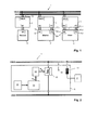
- a bus system for the transmission of data has a supply bus 1 to which on the one hand a number of modules 2 ', 2 "of a device are connected via a transmission unit 3 and on the other hand a power supply unit 4 via a power supply adjustment unit 5 on the other.
- the units 2 ', 2 form the bus subscribers of the bus system, being exemplified in FIG. 1 a master assembly 2 'and a slave assembly 2 "are shown. These assemblies 2', 2" are designed for communication via the I 2 C bus (Inter-Integrated Circuit) and have a connection 6 for a power supply line 7 , On the other hand, the modules 2 ', 2 "each have a connection 8 for a data line I 2 C-1 and a connection 9 for a clock line I 2 C-2 on.
- I 2 C bus Inter-Integrated Circuit
- the power supply module 4 which may be designed as a commercially available power supply, provides a supply voltage of, for example, 5 V of the power supply adaptation unit 5.
- the power supply adjustment unit 5 generates an AC signal 10 which is input to the power supply bus 1.
- the AC voltage signal 10 contains on the one hand a DC component, which is formed by the DC supply voltage of the power supply unit 4.
- the DC voltage of the voltage supply adaptation unit 5 of a coil 11 is fed into the bus 1.
- the supply bus 1 consists on the one hand of a ground line GND and on the other hand from a supply bus VBUS.
- the AC voltage signal 10 has an AC voltage component, so that a synchronization signal S can be introduced into the supply bus 1.
- a carrier signal with a predetermined carrier frequency can be derived or generated in the transmission units 3.
- the voltage supply adaptation unit 5 has a quartz oscillator 12 which generates a clock frequency of 5 MHz.
- the clock frequency is reduced to 250 kHz.
- the rectangular synchronization signal S is converted into a sinusoidal synchronization signal S.
- the feeding of this synchronization signal S by means of a transistor circuit 15 having at least one FET transistor.
- the fed into the supply bus 1 AC signal 10 is thus composed of the synchronization signal S and the supply voltage.
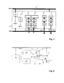
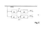
- the transmission unit 3 consists on the one hand of two identically designed transmitting modules 16 ', 16 ", two identically designed receiving modules 17', 17" and a voltage module 18.
- a first transmitting module 16 'and a second receiving module 17' are each connected to the terminal 8 for Data line I 2 C-1 of the units 2 ', 2 "on the one hand and a second transmitter module 16" and a second receiver module 17 “connected to the terminal 9 of the clock line I 2 C-2 of the units 2', 2" on the other.
- the first transmission module 16 'and the first reception module 17' on the one side and the second transmission module 16 “and the second reception module 17” on the other side essentially differ in that they modulate, respectively with carrier signals of different carrier frequency, the signals present at the input demodulate.
- the synchronization filter 19 consists of a bandpass filter which converts the carrier signal applied to the supply bus 1 to the synchronization signal S with a clock frequency of 250 kHz
- This synchronization signal S is sent to a first frequency synthesizer 20 'for generating a first carrier signal 21' with a carrier frequency of 2 MHz of the first transmit module 16 'and a second frequency synthesizer 20 "for generating a second carrier signal 21" with a carrier frequency of 4 MHz of the second Transmitter module 16 "supplied.
- the carrier frequencies of 2 MHz and 4 MHz generated by the frequency synthesizers 20', 20" are present as square-wave voltages and are then fed to a second-order low-pass filter in which they are not shown be converted into sinusoidal carrier signals.
- the transmitter module 16 ' has a first modulator 22', so that the corresponding data are modulated onto the first carrier signal 21 'and then fed to a first feed circuit 23'.
- the data provided by the clock line I 2 C-2 data are modulated by means of a second modulator 22 "of the second transmitting module 16" to the second carrier signal 21 "and fed to a corresponding feed circuit 23" for feeding into the supply bus 1.
- OOK On-Off-Keyling
- a first LOW level is used to transmit the data signal and a second LOW level state is used to receive the data signal.
- a voltage range of 0 V to 0.4 V and for receiving a voltage range of 0.6 V to 1.5 V be set.
- a corresponding comparator upstream of the feed circuits 23 ', 23 " is set.
- the voltage module 18 enables the generation of a positive and a negative supply voltage.
- the negative supply voltage is used for the operation of the components of the transmitting module 16 ', 16 "or receiving module 17', 17".
- the voltage module 18 has a second order passive low-pass filter 28, which is preferably designed as an RLC series resonant circuit.
- the positive supply voltage VBDC + can be provided from the signal present on the supply bus 1.
- a negative voltage VBDC- is generated from the positive voltage VBDC + by means of a voltage inverter 26.
- the data provided by the data line 8 or clock line 9 are stored in the transmission modules 16 ', 16 "of the transmission unit 3 to a carrier signal modulated and transmitted as a modulated transmission signal on the supply bus 1.
- bus subscribers 2 ', 2 can be designed as units of a cash register system or of a cash register machine.
Landscapes
- Engineering & Computer Science (AREA)
- Theoretical Computer Science (AREA)
- Power Engineering (AREA)
- Computer Networks & Wireless Communication (AREA)
- Signal Processing (AREA)
- Physics & Mathematics (AREA)
- General Engineering & Computer Science (AREA)
- General Physics & Mathematics (AREA)
- Small-Scale Networks (AREA)
Applications Claiming Priority (1)
| Application Number | Priority Date | Filing Date | Title |
|---|---|---|---|
| DE200910026207 DE102009026207A1 (de) | 2009-07-20 | 2009-07-20 | Bussystem sowie Verfahren zur Datenübertragung |
Publications (2)
| Publication Number | Publication Date |
|---|---|
| EP2299366A1 true EP2299366A1 (fr) | 2011-03-23 |
| EP2299366B1 EP2299366B1 (fr) | 2014-03-05 |
Family
ID=42782085
Family Applications (1)
| Application Number | Title | Priority Date | Filing Date |
|---|---|---|---|
| EP10401092.1A Active EP2299366B1 (fr) | 2009-07-20 | 2010-06-28 | Bus système et procédé de communication de données |
Country Status (2)
| Country | Link |
|---|---|
| EP (1) | EP2299366B1 (fr) |
| DE (1) | DE102009026207A1 (fr) |
Cited By (2)
| Publication number | Priority date | Publication date | Assignee | Title |
|---|---|---|---|---|
| CN113541737A (zh) * | 2020-04-14 | 2021-10-22 | 湖南迪文科技有限公司 | 一种两线制电源载波通信装置和方法 |
| CN119783134A (zh) * | 2024-12-25 | 2025-04-08 | 无锡翼盟电子科技有限公司 | 一种简易加密方法 |
Citations (3)
| Publication number | Priority date | Publication date | Assignee | Title |
|---|---|---|---|---|
| DE102004046186A1 (de) * | 2004-09-23 | 2006-04-06 | Siemens Ag | Umsetzermodul zur Datenkommunikation über eine Energieversorgungsleitung und Schiff |
| US20080013637A1 (en) * | 2006-04-03 | 2008-01-17 | Matsushita Electric Industrial Co., Ltd. | Multi-carrier communication apparatus, power line communication circuit, and multi-carrier communication method |
| US20080189459A1 (en) * | 2007-02-06 | 2008-08-07 | Seiko Epson Corporation | Serial communication system |
Family Cites Families (3)
| Publication number | Priority date | Publication date | Assignee | Title |
|---|---|---|---|---|
| FR2707024B1 (fr) * | 1993-06-22 | 1995-09-01 | Suisse Electronique Microtech | |
| DE19800457A1 (de) * | 1998-01-08 | 1999-07-22 | Polytrax Inf Technology Ag | Datenübertragung |
| US20080250184A1 (en) * | 2007-04-03 | 2008-10-09 | Vizionware, Inc. | Adaptive two-wire bus |
-
2009
- 2009-07-20 DE DE200910026207 patent/DE102009026207A1/de not_active Withdrawn
-
2010
- 2010-06-28 EP EP10401092.1A patent/EP2299366B1/fr active Active
Patent Citations (3)
| Publication number | Priority date | Publication date | Assignee | Title |
|---|---|---|---|---|
| DE102004046186A1 (de) * | 2004-09-23 | 2006-04-06 | Siemens Ag | Umsetzermodul zur Datenkommunikation über eine Energieversorgungsleitung und Schiff |
| US20080013637A1 (en) * | 2006-04-03 | 2008-01-17 | Matsushita Electric Industrial Co., Ltd. | Multi-carrier communication apparatus, power line communication circuit, and multi-carrier communication method |
| US20080189459A1 (en) * | 2007-02-06 | 2008-08-07 | Seiko Epson Corporation | Serial communication system |
Cited By (2)
| Publication number | Priority date | Publication date | Assignee | Title |
|---|---|---|---|---|
| CN113541737A (zh) * | 2020-04-14 | 2021-10-22 | 湖南迪文科技有限公司 | 一种两线制电源载波通信装置和方法 |
| CN119783134A (zh) * | 2024-12-25 | 2025-04-08 | 无锡翼盟电子科技有限公司 | 一种简易加密方法 |
Also Published As
| Publication number | Publication date |
|---|---|
| EP2299366B1 (fr) | 2014-03-05 |
| DE102009026207A1 (de) | 2011-02-03 |
Similar Documents
| Publication | Publication Date | Title |
|---|---|---|
| DE112009001289B4 (de) | Kommunikationsvorrichtung, Kommunikationssystem und Kommunikationsverfahren | |
| DE69225297T2 (de) | Universelle Übertragungsschnittstelle anpassbar an eine Vielzahl von Schnittstellenstandards | |
| EP0566773B1 (fr) | Procédé et dispositif pour la transmission de données binaires | |
| DE102010003172B4 (de) | Drahtlose Vorrichtung | |
| EP3378198B1 (fr) | Dispositifs et procédé de transmission d'un signal de communication et d'une puissance électrique entre des stations d'abonné d'un système de bus | |
| WO2018149459A1 (fr) | Compensateur, circuit électronique pour faire fonctionner une antenne et dispositif d'antenne | |
| EP2299366B1 (fr) | Bus système et procédé de communication de données | |
| EP4052425B1 (fr) | Procédé, modem et réseau pour la communication entre des dispositifs d'un véhicule | |
| EP1801738B1 (fr) | Transpondeur et méthode pour faire fonctionner un transpondeur | |
| DE102021004854A1 (de) | Verfahren und System zur Datenübertragung | |
| DE4041625C2 (fr) | ||
| EP0874495A2 (fr) | Dispositif de modulation, pour la modulation de signaux numériques | |
| EP3130081B1 (fr) | Systeme de communication en serie, système photovoltaïque et procede de communication en serie | |
| DE2919737A1 (de) | Verfahren und system zur informationsuebertragung | |
| DE102007060228B4 (de) | Übertragungsverfahren sowie Übertragungssystem für Signale unterschiedlicher Datenraten | |
| DE2841764C2 (de) | Wechselstrom-Telegrafie (WT)-Einrichtung | |
| DE1959175A1 (de) | Verfahren zur UEbertragung von n(n = 2,3...) pulsmodulierten Signalen in n Kanaelen | |
| EP0088862A1 (fr) | Système pour le transfert d'un télégramme d'impulsion à grand taux de Baud sur les lignes d'un réseau d'alimentation d'énergie à tension basse | |
| DE4029478C2 (de) | Verfahren zur Übertragung von Daten in einem Bussystem | |
| DE69532933T2 (de) | Telefontrennungsvorrichtung | |
| DE3149956A1 (de) | Linienfunksystem | |
| EP0993134A2 (fr) | Méthode de transmission de signaux d'horloges, méthode de synchronisation de générateurs d'horloges ou d'éléments de réseau, élément de réseau et générateur d'horloge | |
| DE102005035656A1 (de) | ASK-Kommunikationsvorrichtung | |
| DE4014132A1 (de) | Sprachuebertragungssystem | |
| DE4424741A1 (de) | Verfahren und Anordnung zur Übertragung von Daten |
Legal Events
| Date | Code | Title | Description |
|---|---|---|---|
| PUAI | Public reference made under article 153(3) epc to a published international application that has entered the european phase |
Free format text: ORIGINAL CODE: 0009012 |
|
| AK | Designated contracting states |
Kind code of ref document: A1 Designated state(s): AL AT BE BG CH CY CZ DE DK EE ES FI FR GB GR HR HU IE IS IT LI LT LU LV MC MK MT NL NO PL PT RO SE SI SK SM TR |
|
| AX | Request for extension of the european patent |
Extension state: BA ME RS |
|
| 17P | Request for examination filed |
Effective date: 20110603 |
|
| 17Q | First examination report despatched |
Effective date: 20121107 |
|
| GRAP | Despatch of communication of intention to grant a patent |
Free format text: ORIGINAL CODE: EPIDOSNIGR1 |
|
| INTG | Intention to grant announced |
Effective date: 20131111 |
|
| GRAS | Grant fee paid |
Free format text: ORIGINAL CODE: EPIDOSNIGR3 |
|
| GRAA | (expected) grant |
Free format text: ORIGINAL CODE: 0009210 |
|
| AK | Designated contracting states |
Kind code of ref document: B1 Designated state(s): AL AT BE BG CH CY CZ DE DK EE ES FI FR GB GR HR HU IE IS IT LI LT LU LV MC MK MT NL NO PL PT RO SE SI SK SM TR |
|
| REG | Reference to a national code |
Ref country code: GB Ref legal event code: FG4D Free format text: NOT ENGLISH |
|
| REG | Reference to a national code |
Ref country code: CH Ref legal event code: EP |
|
| REG | Reference to a national code |
Ref country code: AT Ref legal event code: REF Ref document number: 655297 Country of ref document: AT Kind code of ref document: T Effective date: 20140315 |
|
| REG | Reference to a national code |
Ref country code: IE Ref legal event code: FG4D Free format text: LANGUAGE OF EP DOCUMENT: GERMAN |
|
| REG | Reference to a national code |
Ref country code: DE Ref legal event code: R096 Ref document number: 502010006248 Country of ref document: DE Effective date: 20140417 |
|
| REG | Reference to a national code |
Ref country code: NL Ref legal event code: VDEP Effective date: 20140305 |
|
| PG25 | Lapsed in a contracting state [announced via postgrant information from national office to epo] |
Ref country code: NO Free format text: LAPSE BECAUSE OF FAILURE TO SUBMIT A TRANSLATION OF THE DESCRIPTION OR TO PAY THE FEE WITHIN THE PRESCRIBED TIME-LIMIT Effective date: 20140605 Ref country code: LT Free format text: LAPSE BECAUSE OF FAILURE TO SUBMIT A TRANSLATION OF THE DESCRIPTION OR TO PAY THE FEE WITHIN THE PRESCRIBED TIME-LIMIT Effective date: 20140305 |
|
| REG | Reference to a national code |
Ref country code: LT Ref legal event code: MG4D |
|
| PG25 | Lapsed in a contracting state [announced via postgrant information from national office to epo] |
Ref country code: SE Free format text: LAPSE BECAUSE OF FAILURE TO SUBMIT A TRANSLATION OF THE DESCRIPTION OR TO PAY THE FEE WITHIN THE PRESCRIBED TIME-LIMIT Effective date: 20140305 Ref country code: CY Free format text: LAPSE BECAUSE OF FAILURE TO SUBMIT A TRANSLATION OF THE DESCRIPTION OR TO PAY THE FEE WITHIN THE PRESCRIBED TIME-LIMIT Effective date: 20140305 Ref country code: FI Free format text: LAPSE BECAUSE OF FAILURE TO SUBMIT A TRANSLATION OF THE DESCRIPTION OR TO PAY THE FEE WITHIN THE PRESCRIBED TIME-LIMIT Effective date: 20140305 |
|
| PG25 | Lapsed in a contracting state [announced via postgrant information from national office to epo] |
Ref country code: HR Free format text: LAPSE BECAUSE OF FAILURE TO SUBMIT A TRANSLATION OF THE DESCRIPTION OR TO PAY THE FEE WITHIN THE PRESCRIBED TIME-LIMIT Effective date: 20140305 Ref country code: LV Free format text: LAPSE BECAUSE OF FAILURE TO SUBMIT A TRANSLATION OF THE DESCRIPTION OR TO PAY THE FEE WITHIN THE PRESCRIBED TIME-LIMIT Effective date: 20140305 |
|
| PG25 | Lapsed in a contracting state [announced via postgrant information from national office to epo] |
Ref country code: NL Free format text: LAPSE BECAUSE OF FAILURE TO SUBMIT A TRANSLATION OF THE DESCRIPTION OR TO PAY THE FEE WITHIN THE PRESCRIBED TIME-LIMIT Effective date: 20140305 Ref country code: EE Free format text: LAPSE BECAUSE OF FAILURE TO SUBMIT A TRANSLATION OF THE DESCRIPTION OR TO PAY THE FEE WITHIN THE PRESCRIBED TIME-LIMIT Effective date: 20140305 Ref country code: IS Free format text: LAPSE BECAUSE OF FAILURE TO SUBMIT A TRANSLATION OF THE DESCRIPTION OR TO PAY THE FEE WITHIN THE PRESCRIBED TIME-LIMIT Effective date: 20140705 Ref country code: BG Free format text: LAPSE BECAUSE OF FAILURE TO SUBMIT A TRANSLATION OF THE DESCRIPTION OR TO PAY THE FEE WITHIN THE PRESCRIBED TIME-LIMIT Effective date: 20140605 Ref country code: RO Free format text: LAPSE BECAUSE OF FAILURE TO SUBMIT A TRANSLATION OF THE DESCRIPTION OR TO PAY THE FEE WITHIN THE PRESCRIBED TIME-LIMIT Effective date: 20140305 Ref country code: CZ Free format text: LAPSE BECAUSE OF FAILURE TO SUBMIT A TRANSLATION OF THE DESCRIPTION OR TO PAY THE FEE WITHIN THE PRESCRIBED TIME-LIMIT Effective date: 20140305 |
|
| PG25 | Lapsed in a contracting state [announced via postgrant information from national office to epo] |
Ref country code: PL Free format text: LAPSE BECAUSE OF FAILURE TO SUBMIT A TRANSLATION OF THE DESCRIPTION OR TO PAY THE FEE WITHIN THE PRESCRIBED TIME-LIMIT Effective date: 20140305 Ref country code: ES Free format text: LAPSE BECAUSE OF FAILURE TO SUBMIT A TRANSLATION OF THE DESCRIPTION OR TO PAY THE FEE WITHIN THE PRESCRIBED TIME-LIMIT Effective date: 20140305 Ref country code: SK Free format text: LAPSE BECAUSE OF FAILURE TO SUBMIT A TRANSLATION OF THE DESCRIPTION OR TO PAY THE FEE WITHIN THE PRESCRIBED TIME-LIMIT Effective date: 20140305 |
|
| REG | Reference to a national code |
Ref country code: DE Ref legal event code: R097 Ref document number: 502010006248 Country of ref document: DE |
|
| PG25 | Lapsed in a contracting state [announced via postgrant information from national office to epo] |
Ref country code: PT Free format text: LAPSE BECAUSE OF FAILURE TO SUBMIT A TRANSLATION OF THE DESCRIPTION OR TO PAY THE FEE WITHIN THE PRESCRIBED TIME-LIMIT Effective date: 20140707 |
|
| PLBE | No opposition filed within time limit |
Free format text: ORIGINAL CODE: 0009261 |
|
| STAA | Information on the status of an ep patent application or granted ep patent |
Free format text: STATUS: NO OPPOSITION FILED WITHIN TIME LIMIT |
|
| PG25 | Lapsed in a contracting state [announced via postgrant information from national office to epo] |
Ref country code: MC Free format text: LAPSE BECAUSE OF FAILURE TO SUBMIT A TRANSLATION OF THE DESCRIPTION OR TO PAY THE FEE WITHIN THE PRESCRIBED TIME-LIMIT Effective date: 20140305 Ref country code: DK Free format text: LAPSE BECAUSE OF FAILURE TO SUBMIT A TRANSLATION OF THE DESCRIPTION OR TO PAY THE FEE WITHIN THE PRESCRIBED TIME-LIMIT Effective date: 20140305 Ref country code: LU Free format text: LAPSE BECAUSE OF FAILURE TO SUBMIT A TRANSLATION OF THE DESCRIPTION OR TO PAY THE FEE WITHIN THE PRESCRIBED TIME-LIMIT Effective date: 20140628 |
|
| REG | Reference to a national code |
Ref country code: CH Ref legal event code: PL |
|
| 26N | No opposition filed |
Effective date: 20141208 |
|
| REG | Reference to a national code |
Ref country code: DE Ref legal event code: R097 Ref document number: 502010006248 Country of ref document: DE Effective date: 20141208 |
|
| REG | Reference to a national code |
Ref country code: IE Ref legal event code: MM4A |
|
| PG25 | Lapsed in a contracting state [announced via postgrant information from national office to epo] |
Ref country code: IT Free format text: LAPSE BECAUSE OF FAILURE TO SUBMIT A TRANSLATION OF THE DESCRIPTION OR TO PAY THE FEE WITHIN THE PRESCRIBED TIME-LIMIT Effective date: 20140305 |
|
| PG25 | Lapsed in a contracting state [announced via postgrant information from national office to epo] |
Ref country code: IE Free format text: LAPSE BECAUSE OF NON-PAYMENT OF DUE FEES Effective date: 20140628 Ref country code: LI Free format text: LAPSE BECAUSE OF NON-PAYMENT OF DUE FEES Effective date: 20140630 Ref country code: CH Free format text: LAPSE BECAUSE OF NON-PAYMENT OF DUE FEES Effective date: 20140630 |
|
| PG25 | Lapsed in a contracting state [announced via postgrant information from national office to epo] |
Ref country code: SI Free format text: LAPSE BECAUSE OF FAILURE TO SUBMIT A TRANSLATION OF THE DESCRIPTION OR TO PAY THE FEE WITHIN THE PRESCRIBED TIME-LIMIT Effective date: 20140305 |
|
| PG25 | Lapsed in a contracting state [announced via postgrant information from national office to epo] |
Ref country code: MT Free format text: LAPSE BECAUSE OF FAILURE TO SUBMIT A TRANSLATION OF THE DESCRIPTION OR TO PAY THE FEE WITHIN THE PRESCRIBED TIME-LIMIT Effective date: 20140305 |
|
| PG25 | Lapsed in a contracting state [announced via postgrant information from national office to epo] |
Ref country code: SM Free format text: LAPSE BECAUSE OF FAILURE TO SUBMIT A TRANSLATION OF THE DESCRIPTION OR TO PAY THE FEE WITHIN THE PRESCRIBED TIME-LIMIT Effective date: 20140305 |
|
| REG | Reference to a national code |
Ref country code: FR Ref legal event code: PLFP Year of fee payment: 7 |
|
| PG25 | Lapsed in a contracting state [announced via postgrant information from national office to epo] |
Ref country code: GR Free format text: LAPSE BECAUSE OF FAILURE TO SUBMIT A TRANSLATION OF THE DESCRIPTION OR TO PAY THE FEE WITHIN THE PRESCRIBED TIME-LIMIT Effective date: 20140606 |
|
| PG25 | Lapsed in a contracting state [announced via postgrant information from national office to epo] |
Ref country code: HU Free format text: LAPSE BECAUSE OF FAILURE TO SUBMIT A TRANSLATION OF THE DESCRIPTION OR TO PAY THE FEE WITHIN THE PRESCRIBED TIME-LIMIT; INVALID AB INITIO Effective date: 20100628 Ref country code: TR Free format text: LAPSE BECAUSE OF FAILURE TO SUBMIT A TRANSLATION OF THE DESCRIPTION OR TO PAY THE FEE WITHIN THE PRESCRIBED TIME-LIMIT Effective date: 20140305 Ref country code: BE Free format text: LAPSE BECAUSE OF FAILURE TO SUBMIT A TRANSLATION OF THE DESCRIPTION OR TO PAY THE FEE WITHIN THE PRESCRIBED TIME-LIMIT Effective date: 20140630 |
|
| REG | Reference to a national code |
Ref country code: AT Ref legal event code: MM01 Ref document number: 655297 Country of ref document: AT Kind code of ref document: T Effective date: 20150628 |
|
| PG25 | Lapsed in a contracting state [announced via postgrant information from national office to epo] |
Ref country code: AT Free format text: LAPSE BECAUSE OF NON-PAYMENT OF DUE FEES Effective date: 20150628 |
|
| REG | Reference to a national code |
Ref country code: FR Ref legal event code: PLFP Year of fee payment: 8 |
|
| REG | Reference to a national code |
Ref country code: FR Ref legal event code: PLFP Year of fee payment: 9 |
|
| PG25 | Lapsed in a contracting state [announced via postgrant information from national office to epo] |
Ref country code: MK Free format text: LAPSE BECAUSE OF FAILURE TO SUBMIT A TRANSLATION OF THE DESCRIPTION OR TO PAY THE FEE WITHIN THE PRESCRIBED TIME-LIMIT Effective date: 20140305 |
|
| PG25 | Lapsed in a contracting state [announced via postgrant information from national office to epo] |
Ref country code: AL Free format text: LAPSE BECAUSE OF FAILURE TO SUBMIT A TRANSLATION OF THE DESCRIPTION OR TO PAY THE FEE WITHIN THE PRESCRIBED TIME-LIMIT Effective date: 20140305 |
|
| REG | Reference to a national code |
Ref country code: FR Ref legal event code: PLFP Year of fee payment: 13 |
|
| REG | Reference to a national code |
Ref country code: GB Ref legal event code: 732E Free format text: REGISTERED BETWEEN 20230323 AND 20230329 |
|
| REG | Reference to a national code |
Ref country code: GB Ref legal event code: 732E Free format text: REGISTERED BETWEEN 20230525 AND 20230601 |
|
| REG | Reference to a national code |
Ref country code: DE Ref legal event code: R081 Ref document number: 502010006248 Country of ref document: DE Owner name: DIEBOLD NIXDORF SYSTEMS GMBH, DE Free format text: FORMER OWNER: WINCOR NIXDORF INTERNATIONAL GMBH, 33106 PADERBORN, DE |
|
| PGFP | Annual fee paid to national office [announced via postgrant information from national office to epo] |
Ref country code: DE Payment date: 20250520 Year of fee payment: 16 |
|
| PGFP | Annual fee paid to national office [announced via postgrant information from national office to epo] |
Ref country code: GB Payment date: 20250520 Year of fee payment: 16 |
|
| PGFP | Annual fee paid to national office [announced via postgrant information from national office to epo] |
Ref country code: FR Payment date: 20250520 Year of fee payment: 16 |