EP2299503A2 - Boîtier de composant luminescent et son procédé de fabrication - Google Patents
Boîtier de composant luminescent et son procédé de fabrication Download PDFInfo
- Publication number
- EP2299503A2 EP2299503A2 EP09750713A EP09750713A EP2299503A2 EP 2299503 A2 EP2299503 A2 EP 2299503A2 EP 09750713 A EP09750713 A EP 09750713A EP 09750713 A EP09750713 A EP 09750713A EP 2299503 A2 EP2299503 A2 EP 2299503A2
- Authority
- EP
- European Patent Office
- Prior art keywords
- light emitting
- semiconductor substrate
- device package
- emitting device
- light
- Prior art date
- Legal status (The legal status is an assumption and is not a legal conclusion. Google has not performed a legal analysis and makes no representation as to the accuracy of the status listed.)
- Withdrawn
Links
Images


Classifications
-
- H—ELECTRICITY
- H10—SEMICONDUCTOR DEVICES; ELECTRIC SOLID-STATE DEVICES NOT OTHERWISE PROVIDED FOR
- H10H—INORGANIC LIGHT-EMITTING SEMICONDUCTOR DEVICES HAVING POTENTIAL BARRIERS
- H10H20/00—Individual inorganic light-emitting semiconductor devices having potential barriers, e.g. light-emitting diodes [LED]
- H10H20/80—Constructional details
- H10H20/81—Bodies
- H10H20/814—Bodies having reflecting means, e.g. semiconductor Bragg reflectors
- H10H20/8142—Bodies having reflecting means, e.g. semiconductor Bragg reflectors forming resonant cavity structures
-
- H—ELECTRICITY
- H10—SEMICONDUCTOR DEVICES; ELECTRIC SOLID-STATE DEVICES NOT OTHERWISE PROVIDED FOR
- H10D—INORGANIC ELECTRIC SEMICONDUCTOR DEVICES
- H10D8/00—Diodes
- H10D8/20—Breakdown diodes, e.g. avalanche diodes
- H10D8/25—Zener diodes
-
- H—ELECTRICITY
- H10—SEMICONDUCTOR DEVICES; ELECTRIC SOLID-STATE DEVICES NOT OTHERWISE PROVIDED FOR
- H10H—INORGANIC LIGHT-EMITTING SEMICONDUCTOR DEVICES HAVING POTENTIAL BARRIERS
- H10H20/00—Individual inorganic light-emitting semiconductor devices having potential barriers, e.g. light-emitting diodes [LED]
- H10H20/80—Constructional details
- H10H20/85—Packages
- H10H20/8506—Containers
-
- H—ELECTRICITY
- H10—SEMICONDUCTOR DEVICES; ELECTRIC SOLID-STATE DEVICES NOT OTHERWISE PROVIDED FOR
- H10H—INORGANIC LIGHT-EMITTING SEMICONDUCTOR DEVICES HAVING POTENTIAL BARRIERS
- H10H20/00—Individual inorganic light-emitting semiconductor devices having potential barriers, e.g. light-emitting diodes [LED]
- H10H20/80—Constructional details
- H10H20/85—Packages
- H10H20/851—Wavelength conversion means
- H10H20/8515—Wavelength conversion means not being in contact with the bodies
-
- H—ELECTRICITY
- H10—SEMICONDUCTOR DEVICES; ELECTRIC SOLID-STATE DEVICES NOT OTHERWISE PROVIDED FOR
- H10H—INORGANIC LIGHT-EMITTING SEMICONDUCTOR DEVICES HAVING POTENTIAL BARRIERS
- H10H20/00—Individual inorganic light-emitting semiconductor devices having potential barriers, e.g. light-emitting diodes [LED]
- H10H20/80—Constructional details
- H10H20/85—Packages
- H10H20/857—Interconnections, e.g. lead-frames, bond wires or solder balls
-
- H—ELECTRICITY
- H10—SEMICONDUCTOR DEVICES; ELECTRIC SOLID-STATE DEVICES NOT OTHERWISE PROVIDED FOR
- H10H—INORGANIC LIGHT-EMITTING SEMICONDUCTOR DEVICES HAVING POTENTIAL BARRIERS
- H10H29/00—Integrated devices, or assemblies of multiple devices, comprising at least one light-emitting semiconductor element covered by group H10H20/00
- H10H29/10—Integrated devices comprising at least one light-emitting semiconductor component covered by group H10H20/00
-
- H—ELECTRICITY
- H10—SEMICONDUCTOR DEVICES; ELECTRIC SOLID-STATE DEVICES NOT OTHERWISE PROVIDED FOR
- H10H—INORGANIC LIGHT-EMITTING SEMICONDUCTOR DEVICES HAVING POTENTIAL BARRIERS
- H10H20/00—Individual inorganic light-emitting semiconductor devices having potential barriers, e.g. light-emitting diodes [LED]
- H10H20/80—Constructional details
- H10H20/85—Packages
- H10H20/851—Wavelength conversion means
-
- H—ELECTRICITY
- H10—SEMICONDUCTOR DEVICES; ELECTRIC SOLID-STATE DEVICES NOT OTHERWISE PROVIDED FOR
- H10H—INORGANIC LIGHT-EMITTING SEMICONDUCTOR DEVICES HAVING POTENTIAL BARRIERS
- H10H20/00—Individual inorganic light-emitting semiconductor devices having potential barriers, e.g. light-emitting diodes [LED]
- H10H20/80—Constructional details
- H10H20/85—Packages
- H10H20/855—Optical field-shaping means, e.g. lenses
- H10H20/856—Reflecting means
Definitions
- the embodiment relates to a light emitting device package and method for manufacturing the same.
- a light emitting device is a semiconductor device to convert a current into a light. Since a red LED has been commercialized, the red LED, together with a green LED, is used as a light source of electronic devices including information communication equipment.
- the light emitting device package includes a light emitting part and a phosphor.
- the light emitting part emits light having a first wavelength and the phosphor emits light having a second wavelength, so that the light emitting device package emitting white light can be realized.
- the light emitted from the phosphor is absorbed into the light emitting part, light efficiency may be reduced.
- color deviation may occur due to the difference of optical paths of the light emitted from the light emitting part and transmitted to the phosphor.
- the embodiment provides a light emitting device package capable of improving light efficiency and reducing color deviation.
- a light emitting device package includes a semiconductor substrate comprising a first surface at a first depth from an upper surface of the semiconductor substrate and a second surface at a second depth from the first surface; and a light emitting part on the second surface of the semiconductor substrate.
- a light emitting device package includes a semiconductor substrate comprising a recess having a multi-layer structure; a light emitting part in the recess of the semiconductor substrate; a first conductive layer electrically connected to a first electrode of the light emitting part; and a second conductive layer electrically connected to a second electrode of the light emitting part.
- the light emitting device package according to the embodiment can improve light efficiency and can reduce color deviation.
- FIG. 18 is a sectional view showing a light emitting device package according to an eighth embodiment.
- each layer is exaggerated, omitted, or schematically illustrated for convenience in description and clarity. Also, the size of each element does not entirely reflect an actual size.
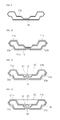
- FIGS. 1 to 11 are sectional views showing the manufacturing process of a light emitting device package according to a first embodiment.
- first and second masks 13 and 15 are formed on upper and lower surfaces of a semiconductor substrate 11.
- a first pattern mask 13a and a second pattern mask 15a are formed.
- the first and second pattern masks 13a and 15a can be formed through a photolithography process.
- the semiconductor substrate 11 can include single crystalline silicon, but the embodiment is not limited thereto.
- the semiconductor substrate 11 can be etched through a dry etching process or a wet etching process.
- the first and second masks 13 and 15 can include a silicon nitride layer, but the embodiment is not limited.
- the semiconductor substrate 11 can be subject to a KOH wet etching process, but the embodiment is not limited thereto.
- the etching process is performed to form a first semiconductor substrate 11 a having a first surface (or first recess) formed at a first depth from an upper surface thereof.
- the etch shape of the first semiconductor substrate 11a can be adjusted according to the alignment of the first and second pattern masks 13a and 15a. Accordingly, the first semiconductor substrate 11a can have the shape of a bathtub with the first surface formed at the first depth from the upper surface of the first semiconductor substrate 11a, but the embodiment is not limited thereto.
- the first and second pattern masks 13a and 15a can be removed from the first semiconductor substrate 11a.
- the first and second pattern masks 13a and 15a can be removed through the wet etching process, but the embodiment is not limited thereto.
- a third mask 17 is formed on the first semiconductor substrate 11a.
- the third mask 17 can include a silicon nitride layer or a silicon oxide layer, but the embodiment is not limited thereto.
- third and fourth pattern masks 17a and 17b are formed on upper and lower surfaces of the first semiconductor substrate 11a.
- the third and fourth pattern masks 17a and 17b can be formed in a desired shape through a photolithography process, but the embodiment is not limited thereto.
- an etching process is performed to form a second semiconductor substrate 11b having a second surface (or a second recess) formed in the first surface at a second depth.
- the etch shape of the second semiconductor substrate 11b can be adjusted according to the alignment of the third and fourth pattern masks 17a and 17b.
- the etching process for the second semiconductor substrate 11b can be performed along to a crystal plane (e.g., (100) or (111)) of a single crystalline substrate.
- the third and fourth pattern masks 17a and 17b can be removed.
- the second semiconductor substrate 11b can have a bathtub shape, in which a first surface A having a first depth h1 on the basis of the upper surface of the semiconductor substrate 11b is formed in a first region and a second surface B having a second depth h2 is formed in a second region of the first surface A.
- an insulating layer 19 can be formed on the second semiconductor substrate 11b.
- the insulating layer 19 is formed for the electric insulation from a conductive layer formed in the subsequent process.
- the insulating layer 19 can include a silicon oxide layer, a silicon nitride layer, an aluminum nitride (AlN) layer, or a silicon carbide (SiC) layer, but the embodiment is not limited thereto.
- the conductive layer can be formed on the insulating layer 19.
- the conductive layer can be electrically connected to a light emitting part that is formed in the subsequent process.
- First and second metal layers 21a and 21b can be formed on the insulating layer 19, and third and fourth metal layers 23a and 23b can be formed below the insulating layer 19.
- a light emitting part 25 can be formed on the second semiconductor substrate 11b.
- the light emitting part 25 can be realized in the form of a light emitting diode, but the embodiment is not limited thereto.
- the first metal layer 21a and/or the third metal layer 23 a serving as a first conductive layer can be connected to a first electrode (not shown) of the light emitting part 25, and the second metal layer 21b and/or the fourth metal layer 23b serving as a second conductive layer can be connected to a second electrode (not shown) of the light emitting part 25.
- the first metal layer 21a and the second metal layer 21 b formed on the upper surface of the second semiconductor substrate 11b can include a metal thin film having high reflectance, so that the light efficiency of the light emitting device package can be improved.
- the third metal layer 23a and the fourth metal layer 23b formed on the lower surface of the second semiconductor substrate 11b can include metal having superior adhesive strength with an adhesive such as a cream solder or the like. This can improve electric/mechanical connection with metal interconnections formed on a printed circuit board in the subsequent surface-mount technology (SMT) process.
- SMT surface-mount technology
- the first and second metal layers 21a and 21b can include a plurality of metal layers, and the upper most layer thereof can include aluminum (Al), silver (Ag), or APC (Ag, Pd, Cu) metal.
- the third and fourth metal layers 23a and 23b can include a plurality of metal layers, and the lower most layer thereof can include gold (Au), or copper (Cu).
- a phosphor 27 can be formed on the light emitting part 25, and a molding part 29 can be formed on the phosphor 27.
- the phosphor 27 can receive light having a first wavelength band from the light emitting part 25 and can supply light having a second wavelength band.
- the second wavelength band can be longer than the first wavelength band.
- White light can be emitted based on the light having the second wavelength band from the phosphor 27 and the light having the first wavelength band from the light emitting part 25.
- the molding part 29 can protect the phosphor 27 and the light emitting part 25.
- the molding part 29 can include silicon, but the embodiment is not limited thereto.
- the light emitting device package can include the second semiconductor substrate 11b, the light emitting part 25, the first metal layer 21a, the second metal layer 21b, the third metal layer 23a, the fourth metal layer 23b, the phosphor 27, the insulating layer 19, and the molding part 29.
- the second semiconductor substrate 11b can be formed in the shape of a two-stage bathtub having the first surface formed at the first depth h1 from the upper surface of the second semiconductor substrate 11b and the second surface formed at the second depth h2 from the first surface.
- the light emitting part 25 can be formed on the second surface of the second semiconductor substrate 11b.
- the first conductive layer including the first metal layer 21a and the third metal layer 23a can be connected to the first electrode of the light emitting part 25, and the second conductive layer including the second metal layer 21b and the fourth metal layer 23b can be connected to the second electrode of the light emitting part 25.
- the first conductive layer can include the first metal layer 21a provided on the semiconductor substrate 11b and the third metal layer 23a provided below the semiconductor substrate 11b.
- the first metal layer 21a and the third metal layer 23a can be electrically connected to each other at an outer peripheral surface of the second semiconductor substrate 11b.
- the second conductive layer can include the second metal layer 21 b provided on the second semiconductor substrate 11b and the fourth metal layer 23b provided below the semiconductor substrate 11b.
- the second metal layer 21b and the fourth metal layer 23b can be electrically connected to each other at the outer peripheral surface of the second semiconductor substrate 11b.
- the phosphor 27 can be formed on the light emitting part 25, and the molding part 29 can be formed on the phosphor 27.
- the insulating layer 19 can be interposed between the semiconductor substrate 11b and the first conductive layer. In addition, the insulating layer 19 can be interposed between the second semiconductor substrate 11b and the second conductive layer.
- a zener diode (not shown) can be formed on the second semiconductor substrate 11b.
- the zener diode can be integrated onto the semiconductor substrate 11b by forming a diode pattern and performing a diffusion process or an ion implantation process for the resultant structure after the insulating layer 19 has been formed, but the embodiment is not limited thereto.
- the zener diode is formed, the withstanding voltage of the light emitting device package according to the embodiment can be improved.
- electronic elements such as a resistor or a capacitor can be integrated into the light emitting device package.
- a mounting region for the light emitting part 25 is formed in the shape of the two-stage bathtub, so that the light emitting part 25 is mounted on the second surface, which is formed at the bottom of the two-stage bathtub, and the first and second metal layers 21a and 21b having high reflectance can be formed on the first surface. Accordingly, light, which is emitted from the light emitting part 25 but cannot be transmitted through a light exit surface (an outer portion of the light emitting device package), is reflected toward the first surface, and light reflected from the first surface is emitted out of the light emitting device package without being incident onto the light emitting part 25, thereby improving light efficiency.
- the distance between a reflective surface, such as a (111) surface formed between the first surface and the second surface, and the light emitting part 25, and the height of the phosphor 27 provided at the upper portion of the light emitting part 25 can be reduced. Accordingly, the light emitted from the light emitting part 25 can be transmitted through the phosphor 27 without causing difference in optical path in all directions around the light emitting part 25, so that color deviation caused by orientation angles of the light can be reduced, thereby supplying high-quality light.
- FIG. 12 is a sectional view showing a light emitting device package according to a second embodiment.
- the light emitting device package according to the second embodiment includes the second semiconductor substrate 11b, the light emitting part 25, the first metal layer 21a, the second metal layer 21b, the third metal layer 23a, the fourth metal layer 23b, a first molding part 31, a second molding part 32, and the insulating layer 19.
- the second embodiment can employ the technical features of the first embodiment, so the second embodiment will be described while focusing on the features distinguished from the first embodiment.
- a phosphor is provided in the second molding part 32.
- the first molding part 31 can be formed on the light emitting part 25, and the second molding part 32 can be formed on the first molding part 31.
- the second molding part 32 can include a second phosphor.
- the first molding part 31 can be filled with transparent silicon gel.
- the first molding part 31 can include a first phosphor.
- the second molding part 32 can include a phosphor, thereby realizing a remove phosphor structure in which the light emitting part 25 is spaced apart from the second molding part 32 including a phosphor to improve light efficiency.
- FIG. 13 is a sectional view showing a light emitting device package according to a third embodiment.
- the third embodiment can employ the technical features of the first embodiment, so that the third embodiment will be described while focusing on the features distinguished from the first embodiment.
- the third embodiment employs a third semiconductor substrate 11c having a first surface in a concave-convex shape.
- a third semiconductor substrate 11c having a first surface in a concave-convex shape For example, when a second surface of the third semiconductor substrate 11c is formed, the second surface having the second depth is formed in a second region of the first surface, and a third surface having a concave-convex shape is formed in a third region of the first surface, thereby forming the third semiconductor substrate 11c having a concave-convex shape as shown in FIG. 13 .
- the concave-convex shape can include a V-shape recess, but the embodiment is not limited thereto.
- the V-shape recess is formed on the first surface, so that light, which does not escape from the light emitting device package but is reflected toward the first surface, is reflected from a concave-convex surface with a changed reflection angle to increase the probability in which the light is emitted from the light emitting device package. Therefore, light efficiency can be more improved.
- FIG. 14 is a sectional view showing a light emitting device package according to a fourth embodiment.
- the fourth embodiment can employ the technical features of the second embodiment, so that the fourth embodiment will be described while focusing on the features distinguished from the second embodiment.
- the first surface of the semiconductor substrate 11c can have a concave-convex pattern according to the fourth embodiment.
- the second surface of the semiconductor substrate 11c when the second surface of the semiconductor substrate 11c is formed, the second surface having the second depth is formed in the second region of the first surface, and a third surface having a concave-convex shape is formed in the third region of the first surface, thereby forming the semiconductor substrate 11c having a concave-convex pattern as shown in FIG. 14 .
- the V-shape recess is formed on the first surface, so that light, which does not escape from the light emitting device package but is reflected toward the first surface, is reflected from a concave-convex surface with a changed reflection angle to increase the probability in which the light is emitted from the light emitting device package. Therefore, light efficiency can be more improved.
- the second molding part 32 includes a phosphor, thereby realizing a remove phosphor structure in which the light emitting part 25 is spaced apart from the second molding part 32 including the phosphor, so that light efficiency can be improved.
- FIG. 15 is a sectional view showing a light emitting device package according to a fifth embodiment.
- the fifth embodiment can employ the technical features of the first embodiment, so that the fifth embodiment will be described while focusing on the features distinguished from the first embodiment.
- the light emitting device package includes a semiconductor substrate 40, a light emitting part 45, a first metal layer 41 a, a second metal layer 41b, a third metal layer 43a, a fourth metal layer 43b, a phosphor 47, an insulating layer 39, and a molding part 49.
- the fifth embodiment has difference in that first and second via holes 53a and 53b are formed in the semiconductor substrate 40.
- the first metal layer 41 a can be electrically connected to the third metal layer 43a through the first via hole 53a formed in the second surface of the semiconductor substrate 40.
- the second metal layer 41b is electrically connected to the fourth metal layer 43b through the second vial hole 53b formed in the second surface of the semiconductor substrate 40.
- the second surface of the semiconductor substrate 40 when the second surface of the semiconductor substrate 40 is formed, the second surface having the second depth is formed in the second region of the first surface, and the first and second vial holes 53a and 53b can be formed in the second surface through the semiconductor substrate 40.
- a desirable etching mask pattern is formed on the upper and lower surfaces of the semiconductor substrate 40, and the etching process for the upper and lower surfaces of the semiconductor substrate 40 is performed, thereby realizing the semiconductor substrate 40 including the first and second via holes 53a and 53b.
- the first conductive layer is electrically connected to the second conductive layer through the first via hole 53a or the second via hole 53b, so that a small-scale light emitting device package can be formed.
- FIG. 16 is a sectional view showing a light emitting device package according to a sixth embodiment.
- the sixth embodiment can employ the technical features of the fifth embodiment, so that the sixth embodiment will be described while focusing on the features distinguished from the fifth embodiment.
- the light emitting device package according to the sixth embodiment can include the semiconductor substrate 40, the light emitting part 45, the first metal layer 41 a, the second metal layer 41b, the third metal layer 43a, the fourth metal layer 43b, a first molding part 51, a second molding part 52, and the insulating layer 39.
- the sixth embodiment can employ the second molding part 52 having a phosphor.
- the first molding part 51 can be formed on the light emitting part 45, and the second molding part 52 can be formed on the first molding part 51.
- the second molding part 52 can include the second phosphor.
- the first molding part 51 can be filled with transparent silicon gel, but the embodiment is not limited thereto.
- the first molding part 31 can include the first phosphor.
- the second molding part 32 includes a phosphor, thereby realizing a remove phosphor structure in which the light emitting part 45 is spaced apart from the second molding part 32 including the phosphor, so that light efficiency can be improved.
- the first conductive layer can be electrically connected to the second conductive layer through the first via hole 53a or the second via hole 53b, so that a small-scale light emitting device package can be formed.
- FIG. 17 is a sectional view showing a light emitting device package according to a seventh embodiment.
- the seventh embodiment can employ the technical features of the fifth embodiment, so that the seventh embodiment will be described while focusing on the features distinguished from the fifth embodiment.
- the seventh embodiment can employ the semiconductor substrate 40 having the first surface in a concave-convex shape.
- the second surface of the semiconductor substrate 40 When the second surface of the semiconductor substrate 40 is formed, the second surface having the second depth can be formed in the second region of the first surface, and the third surface having a concave-convex shape can be formed in the third region of the first surface, so that the semiconductor substrate 40 having a concave-convex shape can be formed.
- the V-shape recess can be formed in the first surface, so that light, which does not escape from the light emitting device package but is reflected toward the first surface, can be reflected from the concave-convex surface with a changed reflection angle to increase the probability in which the light is emitted from the light emitting device package. Therefore, light efficiency can be more improved.
- FIG. 18 is a sectional view showing a light emitting device package according to an eighth embodiment.
- the eighth embodiment can employ the technical features of the sixth embodiment, so that the eighth embodiment will be described while focusing on the features distinguished from the sixth embodiment will be mainly described.
- the eighth embodiment can employ the semiconductor substrate 40 having the first surface in the concave-convex shape.
- the second surface of the semiconductor substrate 40 When the second surface of the semiconductor substrate 40 is formed, the second surface having the second depth can be formed in the second region of the first surface, and the third surface having a concave-convex shape can be formed in the third region of the first surface, so that the semiconductor substrate 40 having a concave-convex shape can be formed.
- the V-shape recess can be formed in the first surface, so that light, which does not escape from the light emitting device package but is reflected toward the first surface, can be reflected from the concave-convex surface with a changed reflection angle to increase the probability in which the light is emitted from the light emitting device package. Therefore, light efficiency can be more improved.
- the second molding part 52 can include a phosphor, thereby realizing a remove phosphor structure in which the light emitting part 45 is spaced apart from the second molding part 52 including the phosphor, so that light efficiency can be improved.
- the light efficiency can be improved, and the color deviation can be reduced.
Landscapes
- Led Device Packages (AREA)
Priority Applications (1)
| Application Number | Priority Date | Filing Date | Title |
|---|---|---|---|
| EP13183420.2A EP2672531B1 (fr) | 2008-05-23 | 2009-04-01 | Emballage de dispositif électroluminescent et son procédé de fabrication |
Applications Claiming Priority (2)
| Application Number | Priority Date | Filing Date | Title |
|---|---|---|---|
| KR1020080048241A KR100992778B1 (ko) | 2008-05-23 | 2008-05-23 | 발광소자 패키지 및 그 제조방법 |
| PCT/KR2009/001665 WO2009142391A2 (fr) | 2008-05-23 | 2009-04-01 | Boîtier de composant luminescent et son procédé de fabrication |
Related Child Applications (1)
| Application Number | Title | Priority Date | Filing Date |
|---|---|---|---|
| EP13183420.2A Division EP2672531B1 (fr) | 2008-05-23 | 2009-04-01 | Emballage de dispositif électroluminescent et son procédé de fabrication |
Publications (2)
| Publication Number | Publication Date |
|---|---|
| EP2299503A2 true EP2299503A2 (fr) | 2011-03-23 |
| EP2299503A4 EP2299503A4 (fr) | 2014-02-05 |
Family
ID=41340649
Family Applications (2)
| Application Number | Title | Priority Date | Filing Date |
|---|---|---|---|
| EP13183420.2A Not-in-force EP2672531B1 (fr) | 2008-05-23 | 2009-04-01 | Emballage de dispositif électroluminescent et son procédé de fabrication |
| EP09750713.1A Withdrawn EP2299503A4 (fr) | 2008-05-23 | 2009-04-01 | Boîtier de composant luminescent et son procédé de fabrication |
Family Applications Before (1)
| Application Number | Title | Priority Date | Filing Date |
|---|---|---|---|
| EP13183420.2A Not-in-force EP2672531B1 (fr) | 2008-05-23 | 2009-04-01 | Emballage de dispositif électroluminescent et son procédé de fabrication |
Country Status (6)
| Country | Link |
|---|---|
| US (6) | US7982237B2 (fr) |
| EP (2) | EP2672531B1 (fr) |
| KR (1) | KR100992778B1 (fr) |
| CN (1) | CN102077372A (fr) |
| DE (1) | DE202009018878U1 (fr) |
| WO (1) | WO2009142391A2 (fr) |
Families Citing this family (42)
| Publication number | Priority date | Publication date | Assignee | Title |
|---|---|---|---|---|
| JP5148849B2 (ja) * | 2006-07-27 | 2013-02-20 | スタンレー電気株式会社 | Ledパッケージ、それを用いた発光装置およびledパッケージの製造方法 |
| JP2010219377A (ja) * | 2009-03-18 | 2010-09-30 | Toshiba Corp | 半導体発光装置及びその製造方法 |
| US8530990B2 (en) | 2009-07-20 | 2013-09-10 | Sunpower Corporation | Optoelectronic device with heat spreader unit |
| US8471289B2 (en) * | 2009-12-28 | 2013-06-25 | Sanyo Electric Co., Ltd. | Semiconductor laser device, optical pickup device and semiconductor device |
| KR101091304B1 (ko) * | 2010-01-20 | 2011-12-07 | 엘지이노텍 주식회사 | 발광 소자 패키지 및 그 제조방법 |
| KR101637581B1 (ko) | 2010-03-09 | 2016-07-07 | 엘지이노텍 주식회사 | 발광 소자 패키지 및 그 제조방법 |
| US8525213B2 (en) * | 2010-03-30 | 2013-09-03 | Lg Innotek Co., Ltd. | Light emitting device having multiple cavities and light unit having the same |
| KR101028329B1 (ko) * | 2010-04-28 | 2011-04-12 | 엘지이노텍 주식회사 | 발광 소자 패키지 및 그 제조방법 |
| KR101039994B1 (ko) | 2010-05-24 | 2011-06-09 | 엘지이노텍 주식회사 | 발광소자 및 이를 구비한 라이트 유닛 |
| US8563849B2 (en) | 2010-08-03 | 2013-10-22 | Sunpower Corporation | Diode and heat spreader for solar module |
| KR101161984B1 (ko) | 2010-08-20 | 2012-07-03 | 엘지이노텍 주식회사 | 발광소자 패키지 |
| US20120112237A1 (en) * | 2010-11-05 | 2012-05-10 | Shenzhen China Star Optoelectronics Technology Co. Ltd. | Led package structure |
| KR20120105146A (ko) * | 2011-03-15 | 2012-09-25 | 삼성전자주식회사 | 발광소자 패키지의 제조장치 및 이를 이용한 발광소자 패키지의 제조방법 |
| CN102694081B (zh) * | 2011-03-21 | 2014-11-05 | 展晶科技(深圳)有限公司 | 发光二极管制造方法 |
| KR101255121B1 (ko) * | 2011-08-10 | 2013-04-22 | 장종진 | 발광 다이오드 패키지 및 그의 제조 방법 |
| KR20130022052A (ko) * | 2011-08-24 | 2013-03-06 | 엘지이노텍 주식회사 | 발광소자 패키지 및 조명 장치 |
| JP5985322B2 (ja) * | 2012-03-23 | 2016-09-06 | 株式会社東芝 | 半導体発光装置及びその製造方法 |
| CN102903838A (zh) * | 2012-07-10 | 2013-01-30 | 贵州大学 | 带散热结构的封装led光源及其制备方法 |
| US8636198B1 (en) | 2012-09-28 | 2014-01-28 | Sunpower Corporation | Methods and structures for forming and improving solder joint thickness and planarity control features for solar cells |
| DE102013203759A1 (de) * | 2013-03-05 | 2014-09-11 | Osram Opto Semiconductors Gmbh | Optoelektronisches Bauelement und elektronisches Gerät mit optoelektronischem Bauelement |
| TW201442290A (zh) * | 2013-04-24 | 2014-11-01 | 鴻海精密工業股份有限公司 | 發光二極體模組 |
| KR102221599B1 (ko) * | 2014-06-18 | 2021-03-02 | 엘지이노텍 주식회사 | 발광 소자 패키지 |
| US9917226B1 (en) | 2016-09-15 | 2018-03-13 | Sharp Kabushiki Kaisha | Substrate features for enhanced fluidic assembly of electronic devices |
| US9722145B2 (en) | 2015-06-24 | 2017-08-01 | Sharp Laboratories Of America, Inc. | Light emitting device and fluidic manufacture thereof |
| US10249599B2 (en) | 2016-06-29 | 2019-04-02 | eLux, Inc. | Laminated printed color conversion phosphor sheets |
| US9755110B1 (en) | 2016-07-27 | 2017-09-05 | Sharp Laboratories Of America, Inc. | Substrate with topological features for steering fluidic assembly LED disks |
| US9985190B2 (en) | 2016-05-18 | 2018-05-29 | eLux Inc. | Formation and structure of post enhanced diodes for orientation control |
| US9892944B2 (en) | 2016-06-23 | 2018-02-13 | Sharp Kabushiki Kaisha | Diodes offering asymmetric stability during fluidic assembly |
| CN104752586A (zh) * | 2015-03-27 | 2015-07-01 | 华南理工大学 | 一种led图形优化封装基板、led封装体及其制备方法 |
| KR102503215B1 (ko) | 2016-03-28 | 2023-02-24 | 삼성전자 주식회사 | 발광 소자 패키지 |
| JP6477734B2 (ja) * | 2016-06-30 | 2019-03-06 | 日亜化学工業株式会社 | 発光装置及びその製造方法 |
| US9627437B1 (en) | 2016-06-30 | 2017-04-18 | Sharp Laboratories Of America, Inc. | Patterned phosphors in through hole via (THV) glass |
| US10243097B2 (en) | 2016-09-09 | 2019-03-26 | eLux Inc. | Fluidic assembly using tunable suspension flow |
| US10378736B2 (en) * | 2016-11-03 | 2019-08-13 | Foshan Nationstar Optoelectronics Co., Ltd. | LED bracket, LED bracket array, LED device and LED display screen |
| US9837390B1 (en) | 2016-11-07 | 2017-12-05 | Corning Incorporated | Systems and methods for creating fluidic assembly structures on a substrate |
| KR102716558B1 (ko) * | 2019-04-30 | 2024-10-15 | 엘지전자 주식회사 | 반도체 발광소자를 이용한 디스플레이 장치 |
| DE102019207714B4 (de) * | 2019-05-27 | 2024-12-12 | Würth Elektronik eiSos Gmbh & Co. KG | Anordnung mit einem SMD-Bauelement und Verfahren zur Herstellung einer Verbindung |
| DE102019207713B4 (de) * | 2019-05-27 | 2024-12-12 | Würth Elektronik eiSos Gmbh & Co. KG | Anordnung mit einem LED-Bauelement und Verfahren zum Herstellen einer Verbindung |
| JP7469592B2 (ja) | 2019-12-05 | 2024-04-17 | 日亜化学工業株式会社 | 発光装置 |
| JP2021110161A (ja) * | 2020-01-10 | 2021-08-02 | 株式会社オーイケ | 壁モジュールおよびそれを有する構造物 |
| CN111613704B (zh) * | 2020-05-29 | 2021-05-18 | 黄山博蓝特半导体科技有限公司 | 一种高亮度深紫外led用图形化蓝宝石衬底及其制备方法 |
| DE102021100546A1 (de) * | 2021-01-13 | 2022-07-14 | OSRAM Opto Semiconductors Gesellschaft mit beschränkter Haftung | Optoelektronisches halbleiterbauelement, optoelektronische vorrichtung sowie verfahren zur herstellung eines optoelektronischen halbleiterbaulements und/oder einer optoelektronischen vorrichtung |
Family Cites Families (110)
| Publication number | Priority date | Publication date | Assignee | Title |
|---|---|---|---|---|
| US5032896A (en) * | 1989-08-31 | 1991-07-16 | Hughes Aircraft Company | 3-D integrated circuit assembly employing discrete chips |
| US5291038A (en) * | 1990-12-19 | 1994-03-01 | Sharp Kabushiki Kaisha | Reflective type photointerrupter |
| DE4242842C2 (de) * | 1992-02-14 | 1999-11-04 | Sharp Kk | Lichtemittierendes Bauelement zur Oberflächenmontage und Verfahren zu dessen Herstellung |
| US5412748A (en) * | 1992-12-04 | 1995-05-02 | Kabushiki Kaisha Toshiba | Optical semiconductor module |
| US5474958A (en) * | 1993-05-04 | 1995-12-12 | Motorola, Inc. | Method for making semiconductor device having no die supporting surface |
| JP2914097B2 (ja) * | 1993-06-25 | 1999-06-28 | 松下電工株式会社 | 射出成形プリント基板 |
| JPH08274378A (ja) | 1995-03-30 | 1996-10-18 | Kyocera Corp | 発光素子収納用パッケージ |
| JPH10319871A (ja) * | 1997-05-19 | 1998-12-04 | Kouha:Kk | Ledディスプレイ装置 |
| JPH1131751A (ja) * | 1997-07-10 | 1999-02-02 | Sony Corp | 中空パッケージとその製造方法 |
| JP2001257410A (ja) | 2000-03-09 | 2001-09-21 | Kyocera Corp | 電子部品 |
| DE10122705B4 (de) * | 2000-05-11 | 2012-07-26 | Mitutoyo Corp. | Einrichtung mit funktionalem Bauelement und Verfahren zu seiner Herstellung |
| DE10041686A1 (de) * | 2000-08-24 | 2002-03-14 | Osram Opto Semiconductors Gmbh | Bauelement mit einer Vielzahl von Lumineszenzdiodenchips |
| KR20020037623A (ko) | 2000-11-15 | 2002-05-22 | 윤종용 | 글라스 리드와 홈이 형성된 글라스 리드 탑재부를 갖는반도체 칩 패키지 |
| US6583447B2 (en) * | 2001-08-27 | 2003-06-24 | Harvatek Corp. | Multiple LED chip package |
| JP4067801B2 (ja) * | 2001-09-18 | 2008-03-26 | 松下電器産業株式会社 | 照明装置 |
| JPWO2003030274A1 (ja) * | 2001-09-27 | 2005-01-20 | 日亜化学工業株式会社 | 発光装置およびその製造方法 |
| US6531328B1 (en) * | 2001-10-11 | 2003-03-11 | Solidlite Corporation | Packaging of light-emitting diode |
| JP4269709B2 (ja) | 2002-02-19 | 2009-05-27 | 日亜化学工業株式会社 | 発光装置およびその製造方法 |
| US6924514B2 (en) * | 2002-02-19 | 2005-08-02 | Nichia Corporation | Light-emitting device and process for producing thereof |
| JP4280038B2 (ja) * | 2002-08-05 | 2009-06-17 | 日亜化学工業株式会社 | 発光装置 |
| KR100961322B1 (ko) | 2002-03-22 | 2010-06-04 | 니치아 카가쿠 고교 가부시키가이샤 | 질화물 형광체와 그 제조 방법 및 발광 장치 |
| JP4407204B2 (ja) | 2002-08-30 | 2010-02-03 | 日亜化学工業株式会社 | 発光装置 |
| JP2004207542A (ja) | 2002-12-26 | 2004-07-22 | Kyocera Corp | 発光素子収納用パッケージおよび発光装置 |
| JP4009208B2 (ja) | 2003-01-21 | 2007-11-14 | 京セラ株式会社 | 発光装置 |
| JP2004281994A (ja) | 2003-01-24 | 2004-10-07 | Kyocera Corp | 発光素子収納用パッケージおよび発光装置 |
| JP2004253711A (ja) | 2003-02-21 | 2004-09-09 | Kyocera Corp | 発光素子収納用パッケージおよび発光装置 |
| KR100517841B1 (ko) * | 2003-02-22 | 2005-09-30 | 주식회사 엠에스솔루션 | 체적탄성파 공진기 밴드 패스 필터, 이를 포함하는듀플렉서 및 그 제조 방법 |
| US6835960B2 (en) * | 2003-03-03 | 2004-12-28 | Opto Tech Corporation | Light emitting diode package structure |
| CN102290409B (zh) * | 2003-04-01 | 2014-01-15 | 夏普株式会社 | 发光装置 |
| JP2004327504A (ja) * | 2003-04-21 | 2004-11-18 | Kyocera Corp | 発光素子収納用パッケージおよび発光装置 |
| JP4070208B2 (ja) | 2003-04-21 | 2008-04-02 | 京セラ株式会社 | 発光素子収納用パッケージおよび発光装置 |
| US7312101B2 (en) * | 2003-04-22 | 2007-12-25 | Micron Technology, Inc. | Packaged microelectronic devices and methods for packaging microelectronic devices |
| US7095053B2 (en) * | 2003-05-05 | 2006-08-22 | Lamina Ceramics, Inc. | Light emitting diodes packaged for high temperature operation |
| US7495322B2 (en) * | 2003-05-26 | 2009-02-24 | Panasonic Electric Works Co., Ltd. | Light-emitting device |
| JP4645071B2 (ja) * | 2003-06-20 | 2011-03-09 | 日亜化学工業株式会社 | パッケージ成型体およびそれを用いた半導体装置 |
| US7183587B2 (en) * | 2003-09-09 | 2007-02-27 | Cree, Inc. | Solid metal block mounting substrates for semiconductor light emitting devices |
| TWI236103B (en) * | 2003-10-28 | 2005-07-11 | South Epitaxy Corp | Flip-chip LED package structure |
| US7652381B2 (en) * | 2003-11-13 | 2010-01-26 | Interconnect Portfolio Llc | Interconnect system without through-holes |
| KR100540848B1 (ko) * | 2004-01-02 | 2006-01-11 | 주식회사 메디아나전자 | 이중 몰드로 구성된 백색 발광다이오드 소자 및 그 제조방법 |
| JP4572312B2 (ja) * | 2004-02-23 | 2010-11-04 | スタンレー電気株式会社 | Led及びその製造方法 |
| JP4504056B2 (ja) * | 2004-03-22 | 2010-07-14 | スタンレー電気株式会社 | 半導体発光装置の製造方法 |
| US7326583B2 (en) | 2004-03-31 | 2008-02-05 | Cree, Inc. | Methods for packaging of a semiconductor light emitting device |
| JP4471356B2 (ja) | 2004-04-23 | 2010-06-02 | スタンレー電気株式会社 | 半導体発光装置 |
| KR100927256B1 (ko) * | 2004-07-09 | 2009-11-16 | 엘지전자 주식회사 | 제너다이오드가 집적된 발광소자 서브마운트 제작방법 |
| JP4254669B2 (ja) * | 2004-09-07 | 2009-04-15 | 豊田合成株式会社 | 発光装置 |
| TWI240438B (en) * | 2004-09-07 | 2005-09-21 | Opto Tech Corp | High power LED array |
| JP2006114854A (ja) * | 2004-10-18 | 2006-04-27 | Sharp Corp | 半導体発光装置、液晶表示装置用のバックライト装置 |
| US20060097385A1 (en) * | 2004-10-25 | 2006-05-11 | Negley Gerald H | Solid metal block semiconductor light emitting device mounting substrates and packages including cavities and heat sinks, and methods of packaging same |
| US7868345B2 (en) | 2004-10-27 | 2011-01-11 | Kyocera Corporation | Light emitting device mounting substrate, light emitting device housing package, light emitting apparatus, and illuminating apparatus |
| JP2008012930A (ja) | 2004-10-27 | 2008-01-24 | Aisin Seiki Co Ltd | シート装置 |
| US7551141B1 (en) * | 2004-11-08 | 2009-06-23 | Alien Technology Corporation | RFID strap capacitively coupled and method of making same |
| JP4061409B2 (ja) * | 2004-11-09 | 2008-03-19 | 国立大学法人九州大学 | センサ部及び生体センサ |
| JP2006135225A (ja) | 2004-11-09 | 2006-05-25 | Toshiba Corp | 発光装置 |
| WO2006098545A2 (fr) * | 2004-12-14 | 2006-09-21 | Seoul Opto Device Co., Ltd. | Dispositif electroluminescent comprenant une pluralite de cellules electroluminescentes, et boitier de support pour ce dispositif |
| JP3872490B2 (ja) | 2004-12-24 | 2007-01-24 | 京セラ株式会社 | 発光素子収納パッケージ、発光装置および照明装置 |
| TWI239670B (en) * | 2004-12-29 | 2005-09-11 | Ind Tech Res Inst | Package structure of light emitting diode and its manufacture method |
| TWI269423B (en) * | 2005-02-02 | 2006-12-21 | Phoenix Prec Technology Corp | Substrate assembly with direct electrical connection as a semiconductor package |
| US7411225B2 (en) * | 2005-03-21 | 2008-08-12 | Lg Electronics Inc. | Light source apparatus |
| KR100593935B1 (ko) * | 2005-03-24 | 2006-06-30 | 삼성전기주식회사 | 발광 다이오드 패키지 및 그 제조 방법 |
| KR100593943B1 (ko) * | 2005-04-30 | 2006-06-30 | 삼성전기주식회사 | 발광 다이오드 패키지의 제조 방법 |
| JP2007049114A (ja) * | 2005-05-30 | 2007-02-22 | Sharp Corp | 発光装置とその製造方法 |
| EP1890343A4 (fr) * | 2005-06-07 | 2014-04-23 | Fujikura Ltd | Substrat pour monter des dispositifs emetteurs de lumiere, module de dispositif emetteur de lumiere, dispositif d'eclairage, dispositif d'affichage et de signalisation de trafic |
| JP2007033698A (ja) * | 2005-07-25 | 2007-02-08 | Fuji Xerox Co Ltd | 光学部品実装用サブマウント、及び光送受信モジュール |
| US20070031992A1 (en) * | 2005-08-05 | 2007-02-08 | Schatz Kenneth D | Apparatuses and methods facilitating functional block deposition |
| KR100600411B1 (ko) | 2005-08-26 | 2006-07-19 | 엘지전자 주식회사 | 발광 소자 패키지 및 그의 제조 방법 |
| US7719099B2 (en) * | 2005-10-21 | 2010-05-18 | Advanced Optoelectronic Technology Inc. | Package structure for solid-state lighting devices and method of fabricating the same |
| KR101171186B1 (ko) * | 2005-11-10 | 2012-08-06 | 삼성전자주식회사 | 고휘도 발광 다이오드 및 이를 이용한 액정 표시 장치 |
| JP2007157940A (ja) * | 2005-12-02 | 2007-06-21 | Nichia Chem Ind Ltd | 発光装置および発光装置の製造方法 |
| JP2007184426A (ja) * | 2006-01-06 | 2007-07-19 | Shinko Electric Ind Co Ltd | 半導体装置の製造方法 |
| JP4925673B2 (ja) | 2006-01-31 | 2012-05-09 | 京セラ株式会社 | 発光装置および発光モジュール |
| JP4817931B2 (ja) | 2006-03-31 | 2011-11-16 | 京セラ株式会社 | 発光装置および発光モジュール |
| JP2007231253A (ja) * | 2006-01-31 | 2007-09-13 | Asahi Glass Co Ltd | 透光封止用硬化性樹脂組成物、樹脂封止発光素子及びその製造方法 |
| US7928462B2 (en) * | 2006-02-16 | 2011-04-19 | Lg Electronics Inc. | Light emitting device having vertical structure, package thereof and method for manufacturing the same |
| JP2007234846A (ja) | 2006-03-01 | 2007-09-13 | Ngk Spark Plug Co Ltd | 発光素子用セラミックパッケージ |
| KR100836210B1 (ko) | 2006-03-22 | 2008-06-09 | (주) 아모센스 | 반도체 패키지 및 그의 제조방법 |
| JP2007273592A (ja) | 2006-03-30 | 2007-10-18 | Kyocera Corp | 発光素子用配線基板および発光装置 |
| JP4960645B2 (ja) | 2006-03-30 | 2012-06-27 | 京セラ株式会社 | 波長変換器および発光装置 |
| JP5091421B2 (ja) * | 2006-04-07 | 2012-12-05 | 株式会社東芝 | 半導体発光装置 |
| KR100735310B1 (ko) * | 2006-04-21 | 2007-07-04 | 삼성전기주식회사 | 다층 반사 면 구조를 갖는 엘이디 패키지 및 그 제조방법 |
| JP2007305703A (ja) | 2006-05-10 | 2007-11-22 | Nichia Chem Ind Ltd | 発光装置 |
| JP2007305785A (ja) * | 2006-05-11 | 2007-11-22 | Nichia Chem Ind Ltd | 発光装置 |
| JP4943739B2 (ja) * | 2006-05-18 | 2012-05-30 | 浜松ホトニクス株式会社 | 光送受信デバイス |
| KR100854328B1 (ko) * | 2006-07-07 | 2008-08-28 | 엘지전자 주식회사 | 발광 소자 패키지 및 그 제조방법 |
| US7960819B2 (en) | 2006-07-13 | 2011-06-14 | Cree, Inc. | Leadframe-based packages for solid state emitting devices |
| TWI320237B (en) * | 2006-07-24 | 2010-02-01 | Si-substrate and structure of opto-electronic package having the same | |
| JP2008053702A (ja) | 2006-07-26 | 2008-03-06 | Kyocera Corp | 発光装置および照明装置 |
| JP5148849B2 (ja) * | 2006-07-27 | 2013-02-20 | スタンレー電気株式会社 | Ledパッケージ、それを用いた発光装置およびledパッケージの製造方法 |
| JP4841348B2 (ja) | 2006-07-27 | 2011-12-21 | 京セラ株式会社 | 発光素子用配線基板および発光装置 |
| US20080029775A1 (en) * | 2006-08-02 | 2008-02-07 | Lustrous Technology Ltd. | Light emitting diode package with positioning groove |
| JP5250949B2 (ja) * | 2006-08-07 | 2013-07-31 | デクセリアルズ株式会社 | 発光素子モジュール |
| KR100792342B1 (ko) | 2006-08-23 | 2008-01-07 | 동부일렉트로닉스 주식회사 | 이미지 센서 제조방법 |
| US7635869B2 (en) * | 2006-09-14 | 2009-12-22 | Lumination Llc | Support with recessed electrically conductive chip attachment material for flip-chip bonding a light emitting chip |
| TWI338385B (en) * | 2006-12-13 | 2011-03-01 | Silicon Base Dev Inc | Side light package structure of light diode and its producing method |
| KR100845856B1 (ko) * | 2006-12-21 | 2008-07-14 | 엘지전자 주식회사 | 발광 소자 패키지 및 그 제조방법 |
| KR100818518B1 (ko) * | 2007-03-14 | 2008-03-31 | 삼성전기주식회사 | Led 패키지 |
| US20080237621A1 (en) * | 2007-03-30 | 2008-10-02 | Sharp Kabushiki Kaisha | Light emitting device and method of producing the same |
| JP5441316B2 (ja) * | 2007-04-05 | 2014-03-12 | ローム株式会社 | 半導体発光装置 |
| CN201066688Y (zh) * | 2007-05-11 | 2008-05-28 | 群康科技(深圳)有限公司 | 发光二极管及背光模组 |
| US7911059B2 (en) * | 2007-06-08 | 2011-03-22 | SeniLEDS Optoelectronics Co., Ltd | High thermal conductivity substrate for a semiconductor device |
| CN101325193B (zh) * | 2007-06-13 | 2010-06-09 | 先进开发光电股份有限公司 | 发光二极管封装体 |
| US20090023234A1 (en) * | 2007-07-17 | 2009-01-22 | Hung-Tsung Hsu | Method for manufacturing light emitting diode package |
| US8288792B2 (en) * | 2008-03-25 | 2012-10-16 | Bridge Semiconductor Corporation | Semiconductor chip assembly with post/base/post heat spreader |
| US8324723B2 (en) | 2008-03-25 | 2012-12-04 | Bridge Semiconductor Corporation | Semiconductor chip assembly with bump/base heat spreader and dual-angle cavity in bump |
| US8415703B2 (en) * | 2008-03-25 | 2013-04-09 | Bridge Semiconductor Corporation | Semiconductor chip assembly with post/base/flange heat spreader and cavity in flange |
| US8212279B2 (en) * | 2008-03-25 | 2012-07-03 | Bridge Semiconductor Corporation | Semiconductor chip assembly with post/base heat spreader, signal post and cavity |
| US20100001305A1 (en) * | 2008-07-07 | 2010-01-07 | Visera Technologies Company Limited | Semiconductor devices and fabrication methods thereof |
| US7928458B2 (en) * | 2008-07-15 | 2011-04-19 | Visera Technologies Company Limited | Light-emitting diode device and method for fabricating the same |
| US7932529B2 (en) * | 2008-08-28 | 2011-04-26 | Visera Technologies Company Limited | Light-emitting diode device and method for fabricating the same |
| US7807484B2 (en) * | 2008-10-15 | 2010-10-05 | Visera Technologies Company Limited | Light-emitting diode device and method for fabricating the same |
| US7928655B2 (en) * | 2008-11-10 | 2011-04-19 | Visera Technologies Company Limited | Light-emitting diode device and method for fabricating the same |
-
2008
- 2008-05-23 KR KR1020080048241A patent/KR100992778B1/ko not_active Expired - Fee Related
-
2009
- 2009-04-01 EP EP13183420.2A patent/EP2672531B1/fr not_active Not-in-force
- 2009-04-01 EP EP09750713.1A patent/EP2299503A4/fr not_active Withdrawn
- 2009-04-01 CN CN2009801251818A patent/CN102077372A/zh active Pending
- 2009-04-01 DE DE202009018878.7U patent/DE202009018878U1/de not_active Expired - Lifetime
- 2009-04-01 WO PCT/KR2009/001665 patent/WO2009142391A2/fr not_active Ceased
- 2009-05-22 US US12/470,787 patent/US7982237B2/en active Active
-
2011
- 2011-06-21 US US13/165,741 patent/US8125000B2/en not_active Expired - Fee Related
-
2012
- 2012-01-10 US US13/347,475 patent/US8592855B2/en not_active Expired - Fee Related
-
2013
- 2013-09-09 US US14/021,577 patent/US8878229B2/en active Active
-
2014
- 2014-10-07 US US14/508,790 patent/US9190450B2/en not_active Expired - Fee Related
-
2015
- 2015-10-26 US US14/923,229 patent/US9455375B2/en active Active
Also Published As
| Publication number | Publication date |
|---|---|
| US7982237B2 (en) | 2011-07-19 |
| US9190450B2 (en) | 2015-11-17 |
| US8878229B2 (en) | 2014-11-04 |
| US9455375B2 (en) | 2016-09-27 |
| CN102077372A (zh) | 2011-05-25 |
| US20110248311A1 (en) | 2011-10-13 |
| KR100992778B1 (ko) | 2010-11-05 |
| KR20090122044A (ko) | 2009-11-26 |
| US20140008696A1 (en) | 2014-01-09 |
| WO2009142391A2 (fr) | 2009-11-26 |
| US8125000B2 (en) | 2012-02-28 |
| US20160049548A1 (en) | 2016-02-18 |
| US20120104447A1 (en) | 2012-05-03 |
| US8592855B2 (en) | 2013-11-26 |
| US20090289272A1 (en) | 2009-11-26 |
| US20150021646A1 (en) | 2015-01-22 |
| EP2672531A2 (fr) | 2013-12-11 |
| EP2672531A3 (fr) | 2014-03-05 |
| EP2672531B1 (fr) | 2020-04-29 |
| DE202009018878U1 (de) | 2014-03-12 |
| EP2299503A4 (fr) | 2014-02-05 |
| WO2009142391A3 (fr) | 2010-01-14 |
Similar Documents
| Publication | Publication Date | Title |
|---|---|---|
| EP2672531B1 (fr) | Emballage de dispositif électroluminescent et son procédé de fabrication | |
| US8766281B2 (en) | Light emitting diode chip, and methods for manufacturing and packaging the same | |
| EP4145543B1 (fr) | Diode électroluminescente | |
| EP2954564B1 (fr) | Composants de diode électroluminescente (del) sans embase et procédés de fabrication associés | |
| US7420221B2 (en) | Semiconductor light-emitting device, lighting module, lighting device and method for manufacturing semiconductor light-emitting device | |
| JP4279388B2 (ja) | 光半導体装置及びその形成方法 | |
| US9559266B2 (en) | Lighting apparatus including an optoelectronic component | |
| JP2020150274A (ja) | 発光デバイスを支持基板に取り付ける方法 | |
| KR101515310B1 (ko) | 발광 다이오드 칩 | |
| TWI517455B (zh) | 發光裝置 | |
| US20120056223A1 (en) | Led package structure and packaging method thereof | |
| KR20180000032A (ko) | 반도체 발광소자 패키지 | |
| CN105322082B (zh) | 发光二极管芯片及发光装置 | |
| KR101578266B1 (ko) | 웨이퍼 레벨 칩 스케일 발광다이오드 패키지 | |
| CN102386318A (zh) | 发光二极管的封装结构及封装方法 | |
| KR101072143B1 (ko) | 발광소자 패키지 및 그 제조방법 | |
| EP2221890B1 (fr) | Conditionnement de dispositif électroluminescent | |
| KR101448588B1 (ko) | 발광 다이오드 패키지 및 그 제조 방법 | |
| JP2017050420A (ja) | 半導体発光装置及びその製造方法 |
Legal Events
| Date | Code | Title | Description |
|---|---|---|---|
| PUAI | Public reference made under article 153(3) epc to a published international application that has entered the european phase |
Free format text: ORIGINAL CODE: 0009012 |
|
| 17P | Request for examination filed |
Effective date: 20101223 |
|
| AK | Designated contracting states |
Kind code of ref document: A2 Designated state(s): AT BE BG CH CY CZ DE DK EE ES FI FR GB GR HR HU IE IS IT LI LT LU LV MC MK MT NL NO PL PT RO SE SI SK TR |
|
| AX | Request for extension of the european patent |
Extension state: AL BA RS |
|
| DAX | Request for extension of the european patent (deleted) | ||
| A4 | Supplementary search report drawn up and despatched |
Effective date: 20140109 |
|
| RIC1 | Information provided on ipc code assigned before grant |
Ipc: H01L 33/50 20100101ALN20140102BHEP Ipc: H01L 33/48 20100101AFI20140102BHEP Ipc: H01L 33/62 20100101ALI20140102BHEP Ipc: H01L 33/60 20100101ALI20140102BHEP |
|
| RAP1 | Party data changed (applicant data changed or rights of an application transferred) |
Owner name: LG INNOTEK CO., LTD. |
|
| STAA | Information on the status of an ep patent application or granted ep patent |
Free format text: STATUS: EXAMINATION IS IN PROGRESS |
|
| 17Q | First examination report despatched |
Effective date: 20181119 |
|
| STAA | Information on the status of an ep patent application or granted ep patent |
Free format text: STATUS: THE APPLICATION IS DEEMED TO BE WITHDRAWN |
|
| 18D | Application deemed to be withdrawn |
Effective date: 20200108 |