EP2301067B1 - Ensembles électrode en pomme de douche pour appareils de traitement plasma - Google Patents
Ensembles électrode en pomme de douche pour appareils de traitement plasma Download PDFInfo
- Publication number
- EP2301067B1 EP2301067B1 EP09762834.1A EP09762834A EP2301067B1 EP 2301067 B1 EP2301067 B1 EP 2301067B1 EP 09762834 A EP09762834 A EP 09762834A EP 2301067 B1 EP2301067 B1 EP 2301067B1
- Authority
- EP
- European Patent Office
- Prior art keywords
- showerhead electrode
- thermal control
- control plate
- particle
- electrode assembly
- Prior art date
- Legal status (The legal status is an assumption and is not a legal conclusion. Google has not performed a legal analysis and makes no representation as to the accuracy of the status listed.)
- Not-in-force
Links
Images


Classifications
-
- C—CHEMISTRY; METALLURGY
- C23—COATING METALLIC MATERIAL; COATING MATERIAL WITH METALLIC MATERIAL; CHEMICAL SURFACE TREATMENT; DIFFUSION TREATMENT OF METALLIC MATERIAL; COATING BY VACUUM EVAPORATION, BY SPUTTERING, BY ION IMPLANTATION OR BY CHEMICAL VAPOUR DEPOSITION, IN GENERAL; INHIBITING CORROSION OF METALLIC MATERIAL OR INCRUSTATION IN GENERAL
- C23C—COATING METALLIC MATERIAL; COATING MATERIAL WITH METALLIC MATERIAL; SURFACE TREATMENT OF METALLIC MATERIAL BY DIFFUSION INTO THE SURFACE, BY CHEMICAL CONVERSION OR SUBSTITUTION; COATING BY VACUUM EVAPORATION, BY SPUTTERING, BY ION IMPLANTATION OR BY CHEMICAL VAPOUR DEPOSITION, IN GENERAL
- C23C16/00—Chemical coating by decomposition of gaseous compounds, without leaving reaction products of surface material in the coating, i.e. chemical vapour deposition [CVD] processes
- C23C16/44—Chemical coating by decomposition of gaseous compounds, without leaving reaction products of surface material in the coating, i.e. chemical vapour deposition [CVD] processes characterised by the method of coating
- C23C16/455—Chemical coating by decomposition of gaseous compounds, without leaving reaction products of surface material in the coating, i.e. chemical vapour deposition [CVD] processes characterised by the method of coating characterised by the method used for introducing gases into reaction chamber or for modifying gas flows in reaction chamber
- C23C16/45563—Gas nozzles
- C23C16/45565—Shower nozzles
-
- H—ELECTRICITY
- H10—SEMICONDUCTOR DEVICES; ELECTRIC SOLID-STATE DEVICES NOT OTHERWISE PROVIDED FOR
- H10P—GENERIC PROCESSES OR APPARATUS FOR THE MANUFACTURE OR TREATMENT OF DEVICES COVERED BY CLASS H10
- H10P50/00—Etching of wafers, substrates or parts of devices
- H10P50/20—Dry etching; Plasma etching; Reactive-ion etching
- H10P50/24—Dry etching; Plasma etching; Reactive-ion etching of semiconductor materials
- H10P50/242—Dry etching; Plasma etching; Reactive-ion etching of semiconductor materials of Group IV materials
-
- C—CHEMISTRY; METALLURGY
- C23—COATING METALLIC MATERIAL; COATING MATERIAL WITH METALLIC MATERIAL; CHEMICAL SURFACE TREATMENT; DIFFUSION TREATMENT OF METALLIC MATERIAL; COATING BY VACUUM EVAPORATION, BY SPUTTERING, BY ION IMPLANTATION OR BY CHEMICAL VAPOUR DEPOSITION, IN GENERAL; INHIBITING CORROSION OF METALLIC MATERIAL OR INCRUSTATION IN GENERAL
- C23C—COATING METALLIC MATERIAL; COATING MATERIAL WITH METALLIC MATERIAL; SURFACE TREATMENT OF METALLIC MATERIAL BY DIFFUSION INTO THE SURFACE, BY CHEMICAL CONVERSION OR SUBSTITUTION; COATING BY VACUUM EVAPORATION, BY SPUTTERING, BY ION IMPLANTATION OR BY CHEMICAL VAPOUR DEPOSITION, IN GENERAL
- C23C16/00—Chemical coating by decomposition of gaseous compounds, without leaving reaction products of surface material in the coating, i.e. chemical vapour deposition [CVD] processes
- C23C16/44—Chemical coating by decomposition of gaseous compounds, without leaving reaction products of surface material in the coating, i.e. chemical vapour deposition [CVD] processes characterised by the method of coating
- C23C16/52—Controlling or regulating the coating process
-
- H—ELECTRICITY
- H01—ELECTRIC ELEMENTS
- H01J—ELECTRIC DISCHARGE TUBES OR DISCHARGE LAMPS
- H01J37/00—Discharge tubes with provision for introducing objects or material to be exposed to the discharge, e.g. for the purpose of examination or processing thereof
- H01J37/32—Gas-filled discharge tubes
- H01J37/32009—Arrangements for generation of plasma specially adapted for examination or treatment of objects, e.g. plasma sources
- H01J37/32082—Radio frequency generated discharge
- H01J37/32091—Radio frequency generated discharge the radio frequency energy being capacitively coupled to the plasma
-
- H—ELECTRICITY
- H01—ELECTRIC ELEMENTS
- H01J—ELECTRIC DISCHARGE TUBES OR DISCHARGE LAMPS
- H01J37/00—Discharge tubes with provision for introducing objects or material to be exposed to the discharge, e.g. for the purpose of examination or processing thereof
- H01J37/32—Gas-filled discharge tubes
- H01J37/32431—Constructional details of the reactor
- H01J37/32532—Electrodes
-
- H—ELECTRICITY
- H01—ELECTRIC ELEMENTS
- H01J—ELECTRIC DISCHARGE TUBES OR DISCHARGE LAMPS
- H01J37/00—Discharge tubes with provision for introducing objects or material to be exposed to the discharge, e.g. for the purpose of examination or processing thereof
- H01J37/32—Gas-filled discharge tubes
- H01J37/32431—Constructional details of the reactor
- H01J37/32532—Electrodes
- H01J37/32541—Shape
-
- H—ELECTRICITY
- H01—ELECTRIC ELEMENTS
- H01J—ELECTRIC DISCHARGE TUBES OR DISCHARGE LAMPS
- H01J37/00—Discharge tubes with provision for introducing objects or material to be exposed to the discharge, e.g. for the purpose of examination or processing thereof
- H01J37/32—Gas-filled discharge tubes
- H01J37/32431—Constructional details of the reactor
- H01J37/32532—Electrodes
- H01J37/32568—Relative arrangement or disposition of electrodes; moving means
-
- H—ELECTRICITY
- H01—ELECTRIC ELEMENTS
- H01J—ELECTRIC DISCHARGE TUBES OR DISCHARGE LAMPS
- H01J37/00—Discharge tubes with provision for introducing objects or material to be exposed to the discharge, e.g. for the purpose of examination or processing thereof
- H01J37/32—Gas-filled discharge tubes
- H01J37/32431—Constructional details of the reactor
- H01J37/32532—Electrodes
- H01J37/32605—Removable or replaceable electrodes or electrode systems
-
- H—ELECTRICITY
- H10—SEMICONDUCTOR DEVICES; ELECTRIC SOLID-STATE DEVICES NOT OTHERWISE PROVIDED FOR
- H10P—GENERIC PROCESSES OR APPARATUS FOR THE MANUFACTURE OR TREATMENT OF DEVICES COVERED BY CLASS H10
- H10P72/00—Handling or holding of wafers, substrates or devices during manufacture or treatment thereof
- H10P72/04—Apparatus for manufacture or treatment
- H10P72/0402—Apparatus for fluid treatment
- H10P72/0418—Apparatus for fluid treatment for etching
- H10P72/0421—Apparatus for fluid treatment for etching for drying etching
Definitions
- semiconductor material processing apparatuses including vacuum processing chambers, are used to perform various processes, such as etching and deposition of various materials on substrates, and resist stripping.
- processes such as etching and deposition of various materials on substrates, and resist stripping.
- semiconductor technology evolves, decreasing device sizes, for example, transistor sizes, call for an ever higher degree of accuracy, repeatability and cleanliness in wafer processes and process equipment.
- Various types of equipment exist for semiconductor processing including applications that involve the use of plasmas, such as plasma etch, plasma-enhanced chemical vapor deposition (PECVD) and resist strip and the like.
- PECVD plasma-enhanced chemical vapor deposition
- resist strip and the like.
- the types of equipment required for these processes include components which are disposed within the plasma chamber, and must function in that environment.
- the environment inside the plasma chamber may include exposure to the plasma, exposure to etchant gasses, and thermal cycling.
- Materials used for such components must be adapted to withstand the environmental conditions in the chamber, and do so for the processing of many wafers which may include multiple process steps per wafer. To be cost effective, such components must often withstand hundreds or thousands of wafer cycles while retaining their functionality and cleanliness. There is generally extremely low tolerance for components which produce particles, even when those particles are few and no larger than a few tens of nanometers. It is also necessary for components selected for use inside plasma processing chambers to meet these requirements in the most cost-effective manner.
- a showerhead electrode assembly as recited in claim 1.
- a vacuum chamber comprising the showerhead electrode assembly of claim 1, as recited in claim 9.
- a third embodiment of the present invention there is a method of controlling plasma etching in a plasma etching chamber using the showerhead electrode assembly of claim 1, as recited in claim 10.
- Plasma processing apparatuses for semiconductor substrates include plasma etch chambers which are used in semiconductor device manufacturing processes to etch such materials as semiconductors, metals and dielectrics.
- a dielectric etch chamber might be used to etch materials such as silicon dioxide or silicon nitride.
- components within the etch chamber heat up and cool down and experience thermal stresses as a result.
- this temperature cycling can result in increased particle generation.
- a showerhead electrode assembly having a heater to prevent the showerhead electrode from falling below a minimum temperature is described in commonly-owned U.S. Patent Publication No. 2005/0133160A1 .
- the heater cooperates with a thermal control plate in heat transfer with a temperature controlled top plate which forms a top wall of a plasma etch chamber.
- FIG. 1 depicts one-half of a showerhead assembly 100 of a parallel plate capacitively-coupled plasma chamber (vacuum chamber) comprising a top electrode 103 and an optional backing member 102 secured to the top electrode 103, a thermal control plate 101, and a top plate 111.
- Thermal chokes 112 can be provided on the upper surface of the thermal control plate 101.
- the top electrode 103 is positioned above a substrate support 160 supporting a semiconductor substrate 162, e.g., semiconductor wafer.
- the top plate 111 can form a removable top wall of the plasma processing apparatus, such as a plasma etch chamber.
- the top electrode 103 can include an inner electrode member 105, and an optional outer electrode member 107.
- the inner electrode member 105 is typically made of single crystal silicon. If desired, the inner and outer electrodes 105, 107 can be made of a single piece of material such as CVD silicon carbide, single crystal silicon or other suitable material.
- the inner electrode member 105 can have a diameter smaller than, equal to, or larger than a wafer to be processed, e.g., up to 200 mm.
- the outer electrode member 107 is adapted to expand the diameter of the top electrode 103 from about 12 inches (about 30.48 cm) to about 19 inches (about 48.26 cm), such as about 15 inches (about 38.1 cm) to about 17 inches (about 43.18 cm).
- the outer electrode member 107 can be a continuous member (e.g., a poly-silicon or silicon carbide member, such as a ring), or a segmented member (e.g., 2-6 separate segments arranged in a ring configuration, such as segments of single crystal silicon).
- the segments preferably have edges which overlap each other to protect an underlying bonding material from exposure to plasma.
- the inner electrode member 105 preferably includes multiple gas passages 104 for injecting a process gas into a space in a plasma reaction chamber below the top electrode 103.
- the outer electrode member 107 can include multiple gas passages (not shown).
- the outer electrode 107 preferably forms a raised step at the periphery of the electrode 103 which does not include gas passages. Further details of a stepped electrode can be found in commonly-owned U.S. Pat. No. 6,824,627 .
- Single crystal silicon is a preferred material for plasma exposed surfaces of the inner electrode member 105 and the outer electrode member 107.
- High-purity, single crystal silicon minimizes contamination of substrates during plasma processing as it introduces only a minimal amount of undesirable elements into the reaction chamber, and also wears smoothly during plasma processing, thereby minimizing particles.
- the showerhead electrode assembly 100 can be sized for processing large substrates, such as semiconductor wafers having a diameter of 300 mm.
- the top electrode 103 is at least 300 mm in diameter.
- the showerhead electrode assembly can be sized to process other wafer sizes or substrates having a non-circular configuration such as substrates for flat panel displays.
- the backing member 102 includes a backing plate 106 and optionally a backing ring 108.
- the inner electrode member 105 is coextensive with the backing plate 106
- the outer electrode member 107 is coextensive with the surrounding backing ring 108.
- the backing plate 106 can extend beyond the inner electrode member such that a single backing plate can be used to support the inner electrode member and the segmented outer electrode member or support a single piece inner electrode and outer electrode.
- the inner electrode member 105 and the outer electrode member 107 are preferably attached to the backing member 102 by a bonding material, such as an elastomeric bonding material.
- the backing plate 106 includes gas passages 113 aligned with the gas passages 104 in the inner electrode member 105 to provide gas flow into the plasma processing chamber. If the outer electrode 107 includes gas passages, the backing ring 108 includes gas passages aligned with such optional gas passages in the outer electrode 107 (not shown).
- the gas passages 113 can typically have a diameter of about 0.04 inch (about 1 mm) and the gas passages 104 can typically have a diameter of about 0.025 inch (about 0.6 mm).
- the backing plate 106 and backing ring 108 are made of an aluminum material, which is typically an aluminum alloy material such as 6061 or other alloy suitable for use in semiconductor processing.
- the backing plate 106 and backing ring 108 can be made of bare aluminum, i.e., aluminum that has a surface native oxide (and is not anodized).
- the top electrode 103 can be attached to the backing plate 106 and backing ring 108 with a thermally and electrically conductive elastomer bonding material that accommodates thermal stresses, and transfers heat and electrical energy between the top electrode 103 and the backing plate 106 and backing ring 108.
- the elastomer can be thermally conductive, but not electrically conductive. The use of elastomers for bonding together surfaces of an electrode assembly is described, for example, in commonly-owned U.S. Pat. No. 6,073,577 .
- the backing plate 106 and the backing ring 108 are preferably attached to the thermal control plate 101 with suitable fasteners, which can be threaded bolts, screws, or the like.
- suitable fasteners can be threaded bolts, screws, or the like.
- bolts (not shown) can be inserted in holes in the thermal control plate 101 and screwed into threaded openings in the backing member 102.
- the thermal control plate 101 is in heat transfer relationship with an actively controlled heater. See, for example, FIGS. 1 and 2 and the description thereof in commonly-owned U.S. Published Application No. 2005/0133160A1 .
- the holes in the thermal control plate 101 can be oversized to allow for movement due to differences in thermal expansion that accommodates thermal stresses.
- the thermal control plate 101 includes a flexure portion 109 and is preferably made of a machined metallic material, such as aluminum, an aluminum alloy such as aluminum alloy 6061 or other alloy suitable for use in semiconductor processing.
- the thermal control plate 101 can be made of bare aluminum, i.e., aluminum that has a surface native oxide (and is not anodized).
- the top plate 111 is preferably made of aluminum or an aluminum alloy such as aluminum alloy 6061.
- a plasma confinement assembly 110 is shown outwardly of the showerhead electrode assembly 100.
- a suitable plasma confinement assembly including a vertically-adjustable, plasma confinement ring assembly is described in commonly-owned U.S. Pat. No. 6,433,484 .
- the thermal control plate 101 preferably includes at least one heater operable to cooperate with the temperature-controlled top plate 111 to control the temperature of the top electrode 103.
- the heater is provided on the upper surface of the thermal control plate 101 and includes a first heater zone surrounded by a first projection 61, a second heater zone between the first projection 61 and a second projection 63, and a third heater zone between the second projection 63 and the flexure portion 109.
- the number of heater zones can be varied; for example, in other embodiments the heater can include a single heater zone, two heater zones, or more than three heater zones.
- the heater can alternatively be provided on a bottom surface of the thermal control plate.
- the heater preferably comprises a laminate including a resistively heated material disposed between opposed layers of a polymeric material that can withstand the operating temperatures reached by the heater.
- a polymeric material that can be used is a polyimide sold under the trademark Kapton®, which is commercially available from E.I. du Pont de Nemours and Company.
- the heater can be a resistive heater embedded in the thermal control plate (e.g., a heating element in a cast thermal control plate or a heating element located in a channel formed in the thermal control plate).
- Another embodiment of the heater includes a resistive heating element mounted on the upper and/or lower surface of the thermal control plate. Heating of the thermal control plate can be achieved via conduction and/or radiation.
- the heater material can have any suitable pattern that provides for thermally uniform heating of the first heater zone, second heater zone, and third heater zone.
- the laminate heater can have a regular or non-regular pattern of resistive heating lines such as a zig-zag, serpentine, or concentric pattern.
- the heater sections located in the first heater zone, second heater zone, and third heater zone can be secured to the thermal control plate by any suitable technique, e.g., the application of heat and pressure, adhesive, fasteners, or the like.
- the top electrode can be electrically grounded, or alternatively can be powered, preferably by a radio-frequency (RF) current source 170.
- the output power of the RF current source 170 powering the top electrode can have a frequency ranging from 50 to 80 MHz, preferably a frequency of 60 MHz, or a similar frequency.
- the bottom electrode can be coupled to the ground potential and the top electrode coupled to the RF source 170.
- the RF source 170 can have a voltage of between about 100 volts and about 2000 volts.
- the top electrode is grounded, and power at one or more frequencies is applied to the bottom electrode to generate plasma in the plasma processing chamber.
- the RF source 170 powering the bottom electrode can have a frequency of between about 400 kHz and about 60 MHz.
- the bottom electrode can be powered at frequencies of 2 MHz and 27 MHz by two independently controlled radio frequency power sources.
- the supply of power to the bottom electrode is shut off to terminate plasma generation.
- the processed substrate is removed from the plasma processing chamber, and another substrate is placed on the substrate support for plasma processing.
- the heater is activated to heat the thermal control plate 101 and, in turn, the top electrode 103, when power to the bottom electrode is shut off.
- the top electrode 103 temperature is preferably prevented from decreasing below a desired minimum temperature.
- the top electrode temperature is preferably maintained at approximately a constant temperature such as 150 to 250°C between successive substrate processing runs so that substrates are processed more uniformly, thereby improving process yields.
- the power supply preferably is controllable to supply power at a desired level and rate to the heater based on the actual temperature and the desired temperature of the top electrode.
- the top electrode 103 can be heated to a temperature of at least about 80°C, such as heating and maintaining at least a portion of the showerhead electrode at a temperature of at least 100°C, at least about 150°C, or at least 180°C.
- the top electrode 103 can be heated before etching of a semiconductor substrate.
- the etching can comprise etching openings in an oxide layer on the semiconductor substrate, where the openings are defined by a patterned photoresist.
- the plasma chamber can also include, for example, a temperature controller; a power supply adapted to supply power to a heater which heats the thermal control plate in thermal response to the temperature controller; a fluid control adapted to supply fluid to a temperature controlled top wall of the chamber in response to the temperature controller; and a temperature sensor arrangement adapted to measure the temperature of one or more portions of the showerhead electrode and supply information to the temperature controller.
- the illustrated embodiment of the showerhead electrode assembly also comprises an aluminum baffle ring arrangement 120 used to distribute process gasses in a plasma chamber.
- the aluminum baffle ring arrangement 120 in FIG. 1 includes six rings made from aluminum or an aluminum alloy, such as 6061 aluminum, which comprises by weight from about 96 to about 98% Al, about 0.8 to about 1.2% Mg, about 0.4 to about 0.8% Si, about 0.15 to 0.4% Cu, about 0.04 to 0.35% Cr, and optionally Fe, Mn, Zn and/or Ti.
- the baffle rings 120 can have an anodized outer surface.
- the six concentric L-shaped rings are located within the plenums above the backing member 102 and below the thermal control plate 101.
- a central plenum can include a single ring
- the adjacent plenum can include two rings separated by a 1/2 to 1 inch (1.27 to 2.54 cm) gap
- the next adjacent plenum can include two rings separated by a 1/2 to 1 inch (1.27 to 2.54 cm) gap
- an outer plenum can include a single ring.
- the rings are mounted to the thermal control plate 101 with screws.
- each ring can include circumferentially spaced apart stand-offs or bosses with through holes for receiving the screws, e.g., three bosses arranged apart can be used.
- Each ring can have a horizontal section of about 0.040 inch (about 1 mm) thickness and a vertical flange of about 1/4 inch (about 0.6 cm) in length.
- the thermal control plate 101 When the top surface 134 of the aluminum backing plate 106 and an annular projection 136 of the thermal control plate 101 come into contact in a contact region 132 during operation of the showerhead electrode assembly 100, galling can occur between the thermal control plate 101 and the aluminum backing member 102 including the backing plate 106 and backing ring 108 along contact regions located between them. Details of galling are described in commonly-owned co-pending U.S. Patent Application No. 11/896,375 .
- the contact regions 132 can cover about 1% to about 30% of the surface area of the backing plate 102.
- galling can occur on both of the thermal control plate 101 and aluminum backing member 102, and is caused by relative motion and rubbing occurring between the opposed surfaces of the thermal control plate 101 and aluminum backing member 102 as a result of temperature cycling. This galling is highly undesirable for a number of reasons. First, galling can cause a reduction in thermal transfer and thus a shift in the temperature including, for example, a localized temperature non-uniformity, of the top electrode 103 including the illustrated inner electrode member 105. This temperature shift can cause a process shift during processing of semiconductor substrates in the plasma processing chamber.
- Galling of the thermal control plate 101 and aluminum backing member 102 can also cause particle generation, or cause fusing of the thermal control plate 101 and aluminum backing member 102, which then requires excessive force to separate these components, which can result in damage to these components.
- Galling of the thermal control plate 101 and aluminum backing member 102 can also increase the difficulty of cleaning the top electrode 103.
- thermal control plate 101 and aluminum backing member 102 degrades the cosmetic appearance of these components and reduces their lifetime.
- FIG. 2 illustrates an exemplary embodiment of the showerhead electrode assembly including a modification that reduces the occurrence of galling of the thermal control plate 101 and aluminum backing plate 106 and backing ring 108 and consequently also reduces problems associated with such galling.
- an interface member 151 which comprises a thermally and electrically conductive gasket 145 and particle mitigating seal portions 147a and 147b, is located between the bottom surface of the annular projection 136 of the thermal control plate and the top surface 134 of the aluminum backing plate 102.
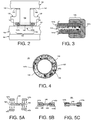
- FIG. 3 shows a cross-section of a portion of an embodiment of an interface member 151.
- the interface member 151 comprises a thermally and electrically conductive gasket portion 145 bounded on a periphery 149 by a particle mitigating seal portion 147a.
- the gasket portion 145 preferably comprises a laminate of coaxial annular rings such as a central portion 143 sandwiched between upper and lower portions 141a and 141b.
- the central portion 143 can be a strip of aluminum and the upper and lower portions 141a/141b can be strips of carbon loaded silicone.
- the gasket portion 145 is a thermal filler material such as a silicone filled with boron nitride (such as CHO-THERM 1671 manufactured by Chomerics), a graphite (such as eGraf 705 manufactured by Graftech), an indium foil, a sandwich (such as Q-pad II by Bergquist), or a phase change material (PCM) (such as T-pcm HP105 by Thermagon).
- boron nitride such as CHO-THERM 1671 manufactured by Chomerics
- a graphite such as eGraf 705 manufactured by Graftech
- an indium foil such as Q-pad II by Bergquist
- a sandwich such as Q-pad II by Bergquist
- PCM phase change material
- the thermally and electrically conductive gasket portion 145 can be, for example, a conductive silicone-aluminum foil sandwich gasket structure, or a elastomer-stainless steel sandwich gasket structure.
- the gasket 145 is Bergquist Q-Pad II composite materials available from The Bergquist Company, located in Chanhassen, Minnesota. These materials comprise aluminum coated on both sides with thermally/electrically conductive rubber. The materials are compatible in vacuum environments.
- the gasket material is preferably also sufficiently compliant so that it compensates for surface roughness of the contact surface and effectively fills regions (e.g., microvoids) of the contact surfaces to enhance thermal contact between the contact surfaces.
- the gasket portion is Lambda Gel COH-4000 (available from Geltec).
- the gaskets can be cleaned using deionized water, such as by wiping.
- the gasket material can alternatively be coated with a suitable coating material, such as a fluoroelastomer material.
- the particle mitigating seal portion 147a/147b can be an elastomer or a polymer resistant to erosion from radicals in a vacuum environment.
- the seal portion 147a/147b is an in-situ cured elastomer or polymer resistant to erosion from radicals produced by plasma in a vacuum environment and resistant to degradation at high temperatures such as above 200°C.
- Polymeric materials which can be used in plasma environments above 160°C include polyimide, polyketone, polyetherketone, polyether sulfone, polyethylene terephthalate, fluoroethylene propylene copolymers, cellulose, triacetates, silicone, and rubber.
- the seal portion 147a/147b is an in-situ room temperature vulcanized (RTV) unfilled silicone exhibiting appropriate pre-cure and post-cure properties such as adhesion strength, elastic modulus, erosion rate, temperature resistance and the like.
- RTV room temperature vulcanized
- an in-situ curable silicone can be a two-part or one-part curing resin using platinum, peroxide or heat.
- the silicone elastomer material has a Si-O backbone with methyl groups (siloxane).
- carbon or carbon-fluorine backbones can also be used.
- the silicone material cures in-situ for isolating the thermally and electrically conductive gasket portion 145 from the vacuum environment in the chamber forming an unfilled, cross-linked silicone rubber.
- An especially preferred elastomer is a polydimethylsiloxane containing elastomer such as a catalyst cured, e.g. Pt-cured, elastomer available from Rhodia as Rhodorsil V217, an elastomer which is stable at temperatures of 250°C and higher.
- the thermally and electrically conductive gasket 145 is made of a material that is electrically conductive (to provide an RF path to the electrode) and thermally conductive to provide electrical and thermal conduction between the thermal control plate 101 and the aluminum backing plate 106.
- the gasket 145 provides an electrically-conductive thermal interface.
- the gasket 145 also enhances heat transfer between the top electrode 103 including the inner electrode member 105 and the thermal control plate 101.
- the particle mitigating seal portion 147a/147b can be dip coated, molded, spray coated or the like onto the periphery 149 of the thermally and electrically conductive gasket portion 145.
- the seal portion 147a/147b is spray coated onto the periphery 149 of the gasket portion 145.
- Spray coating can result in the mitigating seal portion 147a/147b having various cross-sectional shapes (profiles), for example, FIG. 3 shows a mitigating seal portion 147a/147b having a rounded-rectangular cross section.
- the gasket portion 145 can be in the shape of an annular ring having an outward perimeter and an inward aperture where the particle mitigating seal portion 147a and 147b, respectively, is bonded to the gasket portion 145.
- FIG. 4 shows a plan view of an embodiment of an interface member 151 comprising the gasket portion 145 shaped as an annular ring with the seal portion 147a bonded to the outward perimeter 149 and the seal portion 147b bonded to the inner aperture 155.
- Bolt holes 157 are also shown in FIG. 4 , which allow bolts (not shown) to be inserted in holes in the thermal control plate 101 and screwed into threaded openings in the backing plate 106 and backing ring 108 with the interface member 151 located between the bottom surface of the annular projection 136 of the thermal control plate and the top surface 134 of the aluminum backing plate 102.
- the seal portion 147a/147b can be in the form of uncured elastomeric sheets 147c/147d/147e/147f in the shape of annular rings sized to overlap the outward perimeter and the inward aperture of the gasket portion 145.
- the uncured elastomeric sheets 147c/147d/147e/147f can be located on the gasket portion 145 ( FIG. 5B ) and cured to provide an interface member 151 ( FIG. 5C ).
- the particle mitigating seals 147a/147b can be shaped such as O-rings disposed on the outer and inner periphery 149 of each annular gasket portion 145. More generally, (with reference to FIGs. 2 and 4 ) the particle mitigating seal portions 147a/147b of the interface member 151 can have a curved surface and protrude from the outward perimeter 153 and inward aperture 155 of each thermally and electrically conductive gasket portion 145. A plurality of annular projections 136 and annular thermally and electrically conductive gasket portions 145 result in a plurality of seals 147a/147b, for example, from 4 to 20 seal portions 147a/147b.
- the plurality of annular gasket portions 145 require fairly precise placement. Since the interface member 151 provides the particle mitigating seal portions 147a/147b bonded to the periphery 149 of the gasket portion 145, installation of the interface member 151 simplifies precise installation of a thermally and electrically conductive gasket portion 145 sealed off from the vacuum chamber by particle mitigating seal portions 147a/147b. Particularly, when the contact surfaces of the annular gaskets 145 in contact regions 132 are small to allow for variations in location during installation.
- shims 146 having about the same thickness as the gasket 145 are located between the aluminum baffle rings 120 and the bottom surface 142 of the thermal control plate 101.
- the shims 146 can be of a dielectric material.
- the thermal control plate 101 includes several annular projections 136 establishing plenums at the backside of the backing plate 106, e.g., 2 to 10, preferably 4 to 8 projections.
- An interface member 151 is arranged over the contact surfaces of each annular projection.
- FIG. 6 shows another embodiment of an interface member 151' located between the bottom surface of the annular projection 136 of the thermal control plate and the top surface 134 of the aluminum backing plate 102.
- this embodiment of an interface member 151' has a thermally and electrically conductive gasket portion 145' bounded on each periphery by a particle mitigating portion 147a'/147b'.
- the interface member 151' shown in FIG. 6 has an annular thermally and electrically conductive gasket portion 145' bounded on an outer perimeter by a first co-planar particle mitigating seal portion 147a' and bounded on an inner aperture by a second co-planar particle mitigating seal portion 147b'.
- Such an embodiment of a showerhead electrode assembly including the interface member 151' has a fewer number of parts than required if installing a plurality of separate thermally and electrically conductive gaskets and a separate outer and inner seal such as an O-ring, for each thermally and electrically conductive gasket.
- the interface member 151' is easy to install and completely covers contact regions 132.
- a plurality of fasteners (such as 3 to 15 bolts) pass through openings 157 ( FIG. 4 ) in each of the annular gasket portions 145/145' to secure the thermal control plate 101 to the backing plate 106.
- baffles 120 and shims 146 can be omitted if desired.
- first wafer effects refers to secondary heating of subsequent wafers caused indirectly by the heating of the first-processed wafer. Specifically, upon completion of processing of the first wafer, the heated processed wafer and the process chamber side walls radiate heat toward the upper electrode. The upper electrode then indirectly provides a secondary heating mechanism for subsequent wafers that are processed in the chamber.
- the first wafer processed by the system may exhibit a larger than desired critical dimension (CD) variation than subsequent wafers processed by the system since wafer temperature variation can affect CD during etching of high aspect ratio contact vias in semiconductor substrates.
- Subsequently processed wafers may have different and/or less CD variation than the first processed wafer due to stabilization of temperature in the chamber.
- CD critical dimension
- Across-wafer and wafer-to-wafer temperature variation can also be preferably reduced by enhancing thermal transfer through the contact regions 132.
- chamber-to-chamber temperature matching can be preferably achieved where multiple plasma etching chambers in different processing lines are used for a desired process or throughput, by enhancing thermal transfer through the contact regions 132.
- a one degree Centigrade variation in wafer temperature across-wafer, wafer-to-wafer, or chamber-to-chamber can cause a CD variation increase at 3 ⁇ (3x standard deviation) by about 0.5 to 0.1 nm (e.g., 0.4 nm/°C - 0.2 nm/°C or 0.35 nm/°C - 0.25 nm/°C).
- the temperature of subsequently processed wafers can stabilize, such that temperature variation of reference points on subsequently processed wafers is preferably less than about 10 °C, more preferably, less than about 5 °C, such that, for example, the CD variation can be controlled to within about 5 nm (0.5 nm/°C x 10 °C), more preferably, to within about 3 nm (0.3 nm/°C x 10 °C), most preferably to within about 0.5 nm (0.1 nm/°C x 5 °C) for etching high aspect ratio contact vias in semiconductor substrates.
- the CD variation is desirably less than 4 nm at 3 ⁇ .
- the CD variation is preferably, 1 nm or less wafer-to-wafer and 4 nm or less chamber-to-chamber.
- the CD variation is desirably less than 3 nm at 3 ⁇ .
- the CD variation is preferably, 2 nm or less wafer-to-wafer and 4 nm or less chamber-to-chamber.
- the interface members 151/151' minimize temperature shifts from the center of the electrode to the edge of the electrode by less than 10°C and minimize azimuthal temperature shifts to 5 °C or less. Electrode temperature variation due to use of new or used aluminum backing members is related to the contact surface condition of the new and used aluminum backing members.
- the interface members 151/151' preferably can minimize electrode temperature shifts caused by new and used aluminum backing members to less than about 5°C. Also, parts may be removed to be cleaned and it is preferred that a part shows the same thermal performance after such cleaning.
- the interface members 151/151' preferably minimize thermal performance shifts between before and after cleaning of the aluminum backing members to less than about 5°C change in electrode temperature.
- the interface members 151/151' can also reduce or prevent fusing or galling of the thermal control plate 101 and aluminum backing member 102, which allows these components to be separated from each other with minimum force.
- the interface members 151/151' are made of a material that preferably: does not outgas in a high-vacuum environment of, e.g., about 10 to about 200 mTorr; has low particulate generation performance; is compliant to accommodate shear at contact regions; is free of metallic components that are lifetime killers in semiconductor substrates, such as Ag, Ni, Cu and the like; and can minimize the generation of particles during cleaning of the aluminum backing member 102.
- FIG. 7 illustrates a portion of another embodiment of a showerhead electrode assembly.
- the embodiment shown in FIG. 7 does not include a backing member, and the thermal control plate 101 is secured directly to the inner electrode member 105.
- top surface 160 of the top electrode 103 and an annular projection 136 of the thermal control plate 101 come into contact in a contact region 158 during operation of the showerhead electrode assembly 100, galling can occur between the thermal control plate 101 and the top electrode 103 including the inner electrode member 105 and the optional outer electrode member 107 along contact regions located between them.
- This galling can occur on both of the thermal control plate 101 and the top electrode 103, and is caused by relative motion and rubbing occurring between the opposed surfaces of the thermal control plate 101 and the top electrode 103 as a result of temperature cycling.
- This galling is undesirable for reasons similar to those described above in relation to the top surface 134 of the aluminum backing plate 106 and an annular projection 136 of the thermal control plate 101 contacting in a contact region during operation of the showerhead electrode assembly 100.
- galling can cause a reduction in thermal transfer and thus a shift in the temperature including, for example, a localized temperature non-uniformity, of the top electrode 103 including the illustrated inner electrode member 105.
- This temperature shift can cause a process shift during processing such as plasma etching of semiconductor substrates in the plasma processing chamber.
- Galling of the thermal control plate 101 and the top electrode 103 can also cause particle generation, or cause fusing of the thermal control plate 101 and the top electrode 103, which then requires excessive force to separate these components, which can result in damage to these components. Galling of the thermal control plate 101 and the top electrode 103 can also increase the difficulty of cleaning the top electrode 103. Additionally, galling of the thermal control plate 101 and the top electrode 103 degrades the cosmetic appearance of these components and reduces their lifetime.
- the showerhead electrode assembly shown in FIG. 7 can also include an optional outer electrode member, such as the outer electrode member 107 shown in FIG. 1 .
- the outer electrode member can have a ring configuration comprised of a plurality of segments.
- the thermal control plate 101 can be secured directly to the inner electrode member 105 and optional outer electrode member 107 in any suitable manner, such as by fasteners and/or adhesive bonding, such as elastomer bonding. As shown in FIG. 7 , there is a contact region 158 between the top surface 160 of the inner electrode member 105 and the annular projection 136 of the thermal control plate 101.
- the outer surface of the thermal control plate 101 can be anodized except at the surface at the contact region 158, which is of bare aluminum (non-anodized).
- Contact region 158 provides a thermal path to remove heat from the inner electrode member 105 and an RF path for RF power passing through the inner electrode member 105.
- An interface member 151 such as described above with reference to FIG. 2 is provided between the top surface 160 of the inner electrode member 105 and the annular projection 136 of the thermal control plate 101.
- thermally and electrically conductive gasket portion 145 provides a thermal path to remove heat from the inner electrode member 105 and an RF path for RF power passing through the inner electrode member 105.
- Particle mitigating seal portions 147a/147b are bonded to the gasket portion 145 and are disposed in offsets 139 between the aluminum baffle rings 120 and the top surface 160 to form a gas-tight seal.
- the upper ends of the vertical walls of the baffle rings 120 are separated from the bottom surface 142 of the thermal control plate 101 by shims 146.
- the shims 146 are typically made of a dielectric material, such as Kapton®.
- FIG. 8 illustrates an embodiment of an interface member 151' in a showerhead electrode assembly to reduce the occurrence of galling between the thermal control plate 101 and the inner electrode member 105 (and also the optional outer electrode member) along contact regions located between them, and consequently to also reduce problems associated with such galling, such as particle generation.
- galling can cause silicon particle generation and aluminum particle generation.
- the interface member 151' is located between the bottom surface of the annular projection 136 of the thermal control plate 101 and the top surface 160 of the inner electrode member 105.
- the interface member 151' separates adjacent ones of the plenums formed in the thermal control plate 101 from each other.
- the interface member 151' can be made of the same materials as the interface members 151/151' described above with respect to the embodiment of the showerhead electrode assembly shown in FIGs. 6 and 7 .
- the gasket portion 145' material is electrically and thermally conductive to provide electrical and thermal conduction between the thermal control plate 101 and the inner electrode member 105 (and optional outer electrode member), i.e., the gasket 145' provides an electrically-conductive thermal interface between the contact regions.
- shims 146 having about the same thickness as the interface member 151' are located between the aluminum baffle rings 120 and the bottom surface 142 of the thermal control plate 101.
- the shims 146 can be of a dielectric material.
- the interface member 151' allows the aluminum baffles 120 and shims 146 to be omitted if desired.
- the modification to the showerhead electrode assemblies shown in FIGs. 2 and 6-8 reduce the number of parts, simplify installation and completely cover contact regions 132/158, as well as, reduce the occurrence of galling between the thermal control plate 101 and the inner electrode member 105 (and also the optional outer electrode member) along contact regions 132/158 located between them, and consequently also reduce problems associated with such galling, such as particle generation.
- galling can cause silicon particle generation and aluminum particle generation.
- an interface member 151' is located between the bottom surface of the annular projection 136 of the thermal control plate 101 and the top surface 160 of the inner electrode member 105. The interface member 151' separates adjacent ones of the plenums formed in the thermal control plate 101 from each other.
Landscapes
- Chemical & Material Sciences (AREA)
- Engineering & Computer Science (AREA)
- Physics & Mathematics (AREA)
- Plasma & Fusion (AREA)
- Analytical Chemistry (AREA)
- Chemical Kinetics & Catalysis (AREA)
- General Chemical & Material Sciences (AREA)
- Materials Engineering (AREA)
- Mechanical Engineering (AREA)
- Metallurgy (AREA)
- Organic Chemistry (AREA)
- Drying Of Semiconductors (AREA)
- Plasma Technology (AREA)
Claims (15)
- Ensemble électrode en pomme de douche, comprenant :une électrode en pomme de douche adaptée pour être montée dans un intérieur d'une chambre sous vide et alimentée par une énergie radiofréquence (RF) ;une plaque de support (106) fixée à l'électrode en pomme de douche ;une plaque de régulation thermique (101) fixée à la plaque de support (106) via une pluralité de fixations au niveau de multiples régions de contact (132) à travers la plaque de support (106) ; etdes organes d'interface (151) agencés pour séparer la plaque de support (106) et la plaque de régulation thermique (101) au niveau des régions de contact (132), chaque organe d'interface (151) comprenant une portion de joint thermiquement et électriquement conducteur (145) délimitée sur une périphérie par une portion de joint d'étanchéité d'atténuation de particules (147a, 147b), dans lequel la portion de joint d'étanchéité d'atténuation de particules (147a, 147b) est agencée pour être liée à la périphérie (149) de la portion de joint (145).
- Ensemble électrode en pomme de douche selon la revendication 1, dans lequel les régions de contact (132) comprennent des saillies annulaires espacées (136) sur une surface inférieure de la plaque de régulation thermique (101), les organes d'interface (151) comprennent une pluralité d'organes d'interface annulaires (151) dimensionnés pour couvrir les saillies annulaires (136), la portion de joint d'étanchéité d'atténuation de particules (147a, 147b) est agencée pour délimiter la portion de joint thermiquement et électriquement conducteur (145) au niveau d'un périmètre extérieur et d'un orifice intérieur de chaque organe d'interface.
- Ensemble électrode en pomme de douche selon la revendication 2, dans lequel la portion de joint d'étanchéité d'atténuation de particules (147a) située au niveau du périmètre extérieur a une surface incurvée et est agencée pour faire saillie depuis la portion de joint électriquement conducteur (145), et dans lequel la portion de joint d'étanchéité d'atténuation de particules (147b) située au niveau de l'orifice intérieur a une surface incurvée et est agencée pour faire saillie depuis la portion de joint thermiquement et électriquement conducteur (145).
- Ensemble électrode en pomme de douche selon la revendication 1, dans lequel la plaque de régulation thermique (101) et la plaque de support (106) sont réalisées en aluminium non anodisé, la portion de joint thermiquement et électriquement conducteur de l'organe d'interface est un stratifié de matériaux en métal et en polymère, et la portion de joint d'étanchéité d'atténuation de particules (147a, 147b) de l'organe d'interface comprend un élastomère ou polymère résistant à l'érosion.
- Ensemble électrode en pomme de douche selon la revendication 3, comprenant en outre des joints brise-jet (120) en aluminium anodisé dans des plénums entre les saillies annulaires (136), chaque joint brise-jet comportant une paroi verticale adjacente à l'une des saillies annulaires (136), les parois verticales comportant des décalages au niveau d'extrémités inférieures de celles-ci adjacents aux régions de contact (132), et chaque portion de joint d'étanchéité d'atténuation de particules (147a, 147b) étant située dans l'un des décalages de façon à former des joints d'étanchéité sur des côtés opposés des régions de contact (132).
- Ensemble électrode en pomme de douche selon la revendication 5, dans lequel des extrémités supérieures des parois verticales des joints brise-jet sont séparées d'une surface inférieure de la plaque de régulation thermique (101) par des cales (146) ayant environ la même épaisseur que la portion de joint thermiquement et électriquement conducteur de l'organe d'interface.
- Ensemble électrode en pomme de douche selon la revendication 1, comprenant en outre des étranglements thermiques (112) sur une surface supérieure de la plaque de régulation thermique (101).
- Ensemble électrode en pomme de douche selon la revendication 1, dans lequel l'organe d'interface est dépourvu d'argent, de nickel et de cuivre, et les régions de contact (132) sont agencées pour couvrir d'environ 1 % à environ 30 % de la superficie de la plaque de support (106).
- Chambre sous vide comprenant l'ensemble électrode en pomme de douche de la revendication 1, comprenant en outre :un dispositif de régulation de température agencé pour réguler une température d'un ensemble électrode en pomme de douche selon la revendication 1 ;une alimentation électrique adaptée pour alimenter électriquement un élément chauffant agencé pour chauffer la plaque de régulation thermique (101) en réponse thermique au dispositif de régulation de température ;un régulateur de fluide adapté pour fournir un fluide à une paroi supérieure à température régulée de la chambre en réponse au dispositif de régulation de température ; etun agencement de capteur de température adapté pour mesurer la température d'une ou de plusieurs portions de l'électrode en pomme de douche et fournir des informations au dispositif de régulation de température, dans lequel la paroi supérieure de la chambre sous vide est facultativement mise à la terre électriquement.
- Procédé de régulation de gravure au plasma dans une chambre de gravure au plasma, comprenant : la fourniture d'un gaz de traitement à la chambre de gravure au plasma à travers l'ensemble électrode en pomme de douche de la revendication 1, le gaz de traitement s'écoulant dans un écartement entre l'électrode en pomme de douche et une électrode inférieure sur laquelle un substrat semi-conducteur est supporté ; et la gravure d'un substrat semi-conducteur dans la chambre de gravure au plasma en appliquant une puissance radioélectrique à l'électrode en pomme de douche et en excitant le gaz de traitement dans un état de plasma, dans lequel la température de l'électrode en pomme de douche est régulée par la plaque de régulation thermique (101) via une conduction thermique renforcée à travers la portion de joint thermiquement et électriquement conducteur des organes d'interface (151).
- Procédé selon la revendication 10, comprenant en outre le chauffage de l'électrode en pomme de douche à une température d'au moins 80 °C, et facultativement le chauffage et le maintien de l'électrode en pomme de douche à une température d'au moins 100 °C, ou le chauffage et le maintien de l'électrode en pomme de douche à une température d'au moins 180 °C.
- Procédé selon la revendication 10, dans lequel le chauffage de l'électrode en pomme de douche se produit avant la gravure du substrat semi-conducteur, et la gravure comprend des ouvertures de gravure définies par une résine photosensible à motifs dans une couche d'oxyde sur le substrat semi-conducteur, les ouvertures étant définies par une résine photosensible à motifs.
- Ensemble électrode en pomme de douche, comprenant :une électrode en pomme de douche adaptée pour être montée dans un intérieur d'une chambre sous vide ;une plaque de régulation thermique (101) fixée à l'électrode en pomme de douche au niveau de multiples régions de contact (132) à travers l'électrode en pomme de douche avec des plénums entre la plaque de régulation thermique (101) et l'électrode en pomme de douche située entre les régions de contact (132) ; etdes organes d'interface (151) agencés entre l'électrode en pomme de douche et la plaque de régulation thermique (101), au niveau des régions de contact (132), dans lequel chaque organe d'interface comprend une portion de joint thermiquement et électriquement conducteur (145) délimitée sur une périphérie par une portion de joint d'étanchéité d'atténuation de particules (147a, 147b), dans lequel la portion de joint d'étanchéité d'atténuation de particules (147a, 147b) est agencée pour être liée à la périphérie (149) de la portion de joint (145).
- Ensemble électrode en pomme de douche selon la revendication 13, dans lequel : les régions de contact (132) comprennent des surfaces de saillies annulaires espacées (136) prévues sur une surface inférieure de la plaque de régulation thermique (101), les régions de contact (132) sont agencées pour couvrir environ 1 % à environ 30 % de la superficie de l'électrode en pomme de douche ; les organes d'interface (151) comprenant un organe d'interface annulaire situé entre chacune des saillies annulaires (136) et une surface supérieure de l'électrode ; la portion de joint thermiquement et électriquement conducteur de chaque organe d'interface (151) est composée d'un stratifié de matériaux en métal et en polymère dépourvus d'argent, de nickel et de cuivre ; et la portion de joint d'étanchéité d'atténuation de particules (147a, 147b) de chaque organe d'interface est agencée pour délimiter un périmètre extérieur et un orifice intérieur de la portion de joint thermiquement et électriquement conducteur, et est composée de silicone.
- Ensemble électrode en pomme de douche selon la revendication 14, dans lequel : l'électrode en pomme de douche comprend une électrode intérieure et une électrode extérieure, l'électrode intérieure est une plaque circulaire en silicium monocristallin et l'électrode extérieure est une électrode annulaire composée d'une pluralité de segments en silicium monocristallin ; les portions de joint d'étanchéité d'atténuation de particules (147a, 147b) des organes d'interface (151) ont une surface incurvée et sont agencées pour faire saillie depuis le périmètre extérieur et un orifice intérieur de chaque portion de joint thermiquement et électriquement conducteur ; dans lequel l'ensemble électrode en pomme de couche comprend en outre : des joints brise-jet (120) en aluminium anodisé dans des plénums entre les saillies annulaires (136), chaque joint brise-jet comportant une paroi verticale adjacente à l'une des saillies annulaires (136), les parois verticales comportant des décalages au niveau d'extrémités inférieures de celles-ci adjacents aux régions de contact (132) ; et les portions de joint d'étanchéité d'atténuation de particules (147a, 147b) sont situées dans les décalages de façon à former des joints d'étanchéité sur des côtés opposés des régions de contact (132), dans lequel des extrémités supérieures des parois verticales des joints brise-jet sont séparées d'une surface inférieure de la plaque de régulation thermique (101) par des cales (146) ayant environ la même épaisseur que les portions de joint thermiquement et électriquement conducteur des organes d'interface (151).
Applications Claiming Priority (2)
| Application Number | Priority Date | Filing Date | Title |
|---|---|---|---|
| US12/155,739 US8679288B2 (en) | 2008-06-09 | 2008-06-09 | Showerhead electrode assemblies for plasma processing apparatuses |
| PCT/US2009/003186 WO2009151538A1 (fr) | 2008-06-09 | 2009-05-22 | Ensembles électrode en pomme de douche pour appareils de traitement plasma |
Publications (3)
| Publication Number | Publication Date |
|---|---|
| EP2301067A1 EP2301067A1 (fr) | 2011-03-30 |
| EP2301067A4 EP2301067A4 (fr) | 2013-08-28 |
| EP2301067B1 true EP2301067B1 (fr) | 2018-07-11 |
Family
ID=41400708
Family Applications (1)
| Application Number | Title | Priority Date | Filing Date |
|---|---|---|---|
| EP09762834.1A Not-in-force EP2301067B1 (fr) | 2008-06-09 | 2009-05-22 | Ensembles électrode en pomme de douche pour appareils de traitement plasma |
Country Status (7)
| Country | Link |
|---|---|
| US (2) | US8679288B2 (fr) |
| EP (1) | EP2301067B1 (fr) |
| JP (1) | JP5560267B2 (fr) |
| KR (1) | KR101546992B1 (fr) |
| CN (1) | CN102057471B (fr) |
| TW (1) | TWI531682B (fr) |
| WO (1) | WO2009151538A1 (fr) |
Families Citing this family (72)
| Publication number | Priority date | Publication date | Assignee | Title |
|---|---|---|---|---|
| US7645341B2 (en) * | 2003-12-23 | 2010-01-12 | Lam Research Corporation | Showerhead electrode assembly for plasma processing apparatuses |
| US7712434B2 (en) * | 2004-04-30 | 2010-05-11 | Lam Research Corporation | Apparatus including showerhead electrode and heater for plasma processing |
| US8216418B2 (en) * | 2007-06-13 | 2012-07-10 | Lam Research Corporation | Electrode assembly and plasma processing chamber utilizing thermally conductive gasket and o-rings |
| US7862682B2 (en) * | 2007-06-13 | 2011-01-04 | Lam Research Corporation | Showerhead electrode assemblies for plasma processing apparatuses |
| US8187414B2 (en) | 2007-10-12 | 2012-05-29 | Lam Research Corporation | Anchoring inserts, electrode assemblies, and plasma processing chambers |
| US8673080B2 (en) | 2007-10-16 | 2014-03-18 | Novellus Systems, Inc. | Temperature controlled showerhead |
| US8187413B2 (en) * | 2008-03-18 | 2012-05-29 | Lam Research Corporation | Electrode assembly and plasma processing chamber utilizing thermally conductive gasket |
| US8679288B2 (en) * | 2008-06-09 | 2014-03-25 | Lam Research Corporation | Showerhead electrode assemblies for plasma processing apparatuses |
| US8161906B2 (en) * | 2008-07-07 | 2012-04-24 | Lam Research Corporation | Clamped showerhead electrode assembly |
| US8147648B2 (en) * | 2008-08-15 | 2012-04-03 | Lam Research Corporation | Composite showerhead electrode assembly for a plasma processing apparatus |
| US8869741B2 (en) * | 2008-12-19 | 2014-10-28 | Lam Research Corporation | Methods and apparatus for dual confinement and ultra-high pressure in an adjustable gap plasma chamber |
| US8272346B2 (en) * | 2009-04-10 | 2012-09-25 | Lam Research Corporation | Gasket with positioning feature for clamped monolithic showerhead electrode |
| US9111729B2 (en) | 2009-12-03 | 2015-08-18 | Lam Research Corporation | Small plasma chamber systems and methods |
| US9190289B2 (en) | 2010-02-26 | 2015-11-17 | Lam Research Corporation | System, method and apparatus for plasma etch having independent control of ion generation and dissociation of process gas |
| US8529729B2 (en) | 2010-06-07 | 2013-09-10 | Lam Research Corporation | Plasma processing chamber component having adaptive thermal conductor |
| KR101189905B1 (ko) * | 2010-07-13 | 2012-10-10 | 플란제 에스이 | 전극용 플라즈마 실드 |
| US9449793B2 (en) | 2010-08-06 | 2016-09-20 | Lam Research Corporation | Systems, methods and apparatus for choked flow element extraction |
| US9155181B2 (en) | 2010-08-06 | 2015-10-06 | Lam Research Corporation | Distributed multi-zone plasma source systems, methods and apparatus |
| US9967965B2 (en) | 2010-08-06 | 2018-05-08 | Lam Research Corporation | Distributed, concentric multi-zone plasma source systems, methods and apparatus |
| US8999104B2 (en) | 2010-08-06 | 2015-04-07 | Lam Research Corporation | Systems, methods and apparatus for separate plasma source control |
| US20120073752A1 (en) * | 2010-09-24 | 2012-03-29 | Memc Electronic Materials, Inc. | Adapter Ring For Silicon Electrode |
| SG192967A1 (en) | 2011-03-04 | 2013-09-30 | Novellus Systems Inc | Hybrid ceramic showerhead |
| US9177762B2 (en) | 2011-11-16 | 2015-11-03 | Lam Research Corporation | System, method and apparatus of a wedge-shaped parallel plate plasma reactor for substrate processing |
| US10283325B2 (en) | 2012-10-10 | 2019-05-07 | Lam Research Corporation | Distributed multi-zone plasma source systems, methods and apparatus |
| US9083182B2 (en) | 2011-11-21 | 2015-07-14 | Lam Research Corporation | Bypass capacitors for high voltage bias power in the mid frequency RF range |
| US8872525B2 (en) | 2011-11-21 | 2014-10-28 | Lam Research Corporation | System, method and apparatus for detecting DC bias in a plasma processing chamber |
| US10586686B2 (en) | 2011-11-22 | 2020-03-10 | Law Research Corporation | Peripheral RF feed and symmetric RF return for symmetric RF delivery |
| US8898889B2 (en) | 2011-11-22 | 2014-12-02 | Lam Research Corporation | Chuck assembly for plasma processing |
| US9396908B2 (en) | 2011-11-22 | 2016-07-19 | Lam Research Corporation | Systems and methods for controlling a plasma edge region |
| US9263240B2 (en) | 2011-11-22 | 2016-02-16 | Lam Research Corporation | Dual zone temperature control of upper electrodes |
| SG11201402553UA (en) * | 2011-11-23 | 2014-09-26 | Lam Res Corp | Dual zone temperature control of upper electrodes |
| KR101971312B1 (ko) * | 2011-11-23 | 2019-04-22 | 램 리써치 코포레이션 | 다중 존 가스 주입 상부 전극 시스템 |
| KR102011535B1 (ko) | 2011-11-24 | 2019-08-16 | 램 리써치 코포레이션 | 가요성 있는 대칭적 rf 복귀 스트랩을 갖는 플라즈마 프로세싱 챔버 |
| US9982340B2 (en) | 2012-04-04 | 2018-05-29 | Taiwan Semiconductor Manufacturing Co. Ltd. | Shower head apparatus and method for controlling plasma or gas distribution |
| JP2013254901A (ja) * | 2012-06-08 | 2013-12-19 | Toshiba Corp | シール材およびエッチング装置 |
| CN103903946B (zh) * | 2012-12-26 | 2017-11-17 | 中微半导体设备(上海)有限公司 | 一种用于等离子反应器的气体喷淋头 |
| US9610591B2 (en) | 2013-01-25 | 2017-04-04 | Applied Materials, Inc. | Showerhead having a detachable gas distribution plate |
| US10741365B2 (en) * | 2014-05-05 | 2020-08-11 | Lam Research Corporation | Low volume showerhead with porous baffle |
| US9911579B2 (en) | 2014-07-03 | 2018-03-06 | Applied Materials, Inc. | Showerhead having a detachable high resistivity gas distribution plate |
| US9859088B2 (en) * | 2015-04-30 | 2018-01-02 | Lam Research Corporation | Inter-electrode gap variation methods for compensating deposition non-uniformity |
| US10378107B2 (en) | 2015-05-22 | 2019-08-13 | Lam Research Corporation | Low volume showerhead with faceplate holes for improved flow uniformity |
| US10023959B2 (en) | 2015-05-26 | 2018-07-17 | Lam Research Corporation | Anti-transient showerhead |
| US10373810B2 (en) | 2016-02-21 | 2019-08-06 | Applied Materials, Inc. | Showerhead having an extended detachable gas distribution plate |
| KR101855654B1 (ko) * | 2016-12-23 | 2018-05-08 | 주식회사 테스 | 대면적 샤워헤드 어셈블리 |
| FR3061914B1 (fr) * | 2017-01-16 | 2019-05-31 | Kobus Sas | Chambre de traitement pour un reacteur de depot chimique en phase vapeur (cvd) et procede de thermalisation mis en œuvre dans cette chambre |
| JP6278498B1 (ja) * | 2017-05-19 | 2018-02-14 | 日本新工芯技株式会社 | リング状部材の製造方法及びリング状部材 |
| US11380557B2 (en) * | 2017-06-05 | 2022-07-05 | Applied Materials, Inc. | Apparatus and method for gas delivery in semiconductor process chambers |
| US20180366354A1 (en) * | 2017-06-19 | 2018-12-20 | Applied Materials, Inc. | In-situ semiconductor processing chamber temperature apparatus |
| TWI788390B (zh) * | 2017-08-10 | 2023-01-01 | 美商應用材料股份有限公司 | 用於電漿處理的分佈式電極陣列 |
| US20190048467A1 (en) * | 2017-08-10 | 2019-02-14 | Applied Materials, Inc. | Showerhead and process chamber incorporating same |
| CN109616813B (zh) * | 2017-09-29 | 2020-05-22 | 中微半导体设备(上海)股份有限公司 | 一种侧装结构及其安装方法及接地环侧装的刻蚀装置 |
| US10964514B2 (en) * | 2017-10-17 | 2021-03-30 | Lam Research Corporation | Electrode for plasma processing chamber |
| KR102256691B1 (ko) * | 2017-10-24 | 2021-05-26 | 세메스 주식회사 | 기판 처리 장치 및 방법 |
| KR20210018232A (ko) * | 2018-06-07 | 2021-02-17 | 도쿄엘렉트론가부시키가이샤 | 기판 처리 장치 및 샤워 헤드 |
| CN108760828B (zh) * | 2018-08-15 | 2023-07-28 | 河北科瑞达仪器科技股份有限公司 | 一种用于液体电导率测量的装置 |
| CN110942969B (zh) * | 2018-09-21 | 2022-08-23 | 中微半导体设备(上海)股份有限公司 | 一种气体喷淋头组件及其等离子体处理设备 |
| CN111383892B (zh) * | 2018-12-29 | 2023-03-07 | 中微半导体设备(上海)股份有限公司 | 等离子体处理装置中气体喷淋头的接地连接结构 |
| CN111524775B (zh) * | 2019-02-01 | 2023-03-10 | 中微半导体设备(上海)股份有限公司 | 一种等离子处理器以及用于等离子处理器的上电极组件 |
| JP7715643B2 (ja) | 2019-05-31 | 2025-07-30 | グリーン, ツイード テクノロジーズ, インコーポレイテッド | 半導体弁において有用であるシール特性の監視および分析のためのスマートシール |
| US10954595B2 (en) * | 2019-07-30 | 2021-03-23 | Applied Materials, Inc. | High power showerhead with recursive gas flow distribution |
| KR20260046529A (ko) | 2019-08-23 | 2026-04-07 | 램 리써치 코포레이션 | 열 제어된 샹들리에 샤워헤드 |
| CN119980191A (zh) | 2019-08-28 | 2025-05-13 | 朗姆研究公司 | 金属沉积 |
| JP7296829B2 (ja) * | 2019-09-05 | 2023-06-23 | 東京エレクトロン株式会社 | プラズマ処理装置、処理方法、上部電極構造 |
| CN113035679B (zh) * | 2019-12-24 | 2023-09-29 | 中微半导体设备(上海)股份有限公司 | 一种等离子体处理装置 |
| US20210238745A1 (en) * | 2020-02-03 | 2021-08-05 | Applied Materials, Inc. | Showerhead assembly |
| US11555250B2 (en) * | 2020-04-29 | 2023-01-17 | Applied Materials, Inc. | Organic contamination free surface machining |
| CN114188206B (zh) * | 2020-09-15 | 2023-09-29 | 中微半导体设备(上海)股份有限公司 | 一种等离子体处理装置及其上电极组件的调节方法 |
| US20220223384A1 (en) * | 2021-01-14 | 2022-07-14 | Samsung Electronics Co., Ltd. | Apparatus for manufacturing a semiconductor device |
| CN120380193A (zh) * | 2022-07-08 | 2025-07-25 | 东曹Smd有限公司 | 用于物理气相沉积溅射应用的动态真空密封系统 |
| KR20250059504A (ko) * | 2022-09-07 | 2025-05-02 | 램 리써치 코포레이션 | 플라즈마 프로세싱을 위해 성형된 실리콘 외측 상부 전극 |
| CN116288273A (zh) * | 2023-03-10 | 2023-06-23 | 拓荆科技(上海)有限公司 | 喷淋头、加热气体的方法、半导体器件的加工设备及方法 |
| USD1109856S1 (en) | 2023-07-07 | 2026-01-20 | Tosoh Smd, Inc. | Dynamic vacuum seal system isolation ring for physical vapor deposition sputter applications |
Family Cites Families (58)
| Publication number | Priority date | Publication date | Assignee | Title |
|---|---|---|---|---|
| US701726A (en) * | 1901-12-30 | 1902-06-03 | George F Hodkinson | Filter. |
| US4654754A (en) | 1982-11-02 | 1987-03-31 | Fairchild Weston Systems, Inc. | Thermal link |
| US4598249A (en) * | 1984-02-29 | 1986-07-01 | Rca Corporation | Method using surface photovoltage (SPV) measurements for revealing heavy metal contamination of semiconductor material |
| US4782893A (en) | 1986-09-15 | 1988-11-08 | Trique Concepts, Inc. | Electrically insulating thermally conductive pad for mounting electronic components |
| US4960612A (en) * | 1987-07-02 | 1990-10-02 | At&T Bell Laboratories | Thermal conductor assembly method |
| US6063233A (en) | 1991-06-27 | 2000-05-16 | Applied Materials, Inc. | Thermal control apparatus for inductively coupled RF plasma reactor having an overhead solenoidal antenna |
| EP0661916B1 (fr) | 1993-07-06 | 2000-05-17 | Kabushiki Kaisha Toshiba | Feuille thermoconductrice |
| CA2129073C (fr) | 1993-09-10 | 2007-06-05 | John P. Kalinoski | Joints moulants iem |
| DE4339786C5 (de) | 1993-11-18 | 2004-02-05 | Emi-Tec Elektronische Materialien Gmbh | Verfahren zur Herstellung einer Anordung zur Wärmeableitung |
| US5545473A (en) | 1994-02-14 | 1996-08-13 | W. L. Gore & Associates, Inc. | Thermally conductive interface |
| US5893796A (en) | 1995-03-28 | 1999-04-13 | Applied Materials, Inc. | Forming a transparent window in a polishing pad for a chemical mechanical polishing apparatus |
| US5679457A (en) | 1995-05-19 | 1997-10-21 | The Bergquist Company | Thermally conductive interface for electronic devices |
| US5534751A (en) | 1995-07-10 | 1996-07-09 | Lam Research Corporation | Plasma etching apparatus utilizing plasma confinement |
| JP3113796B2 (ja) | 1995-07-10 | 2000-12-04 | 東京エレクトロン株式会社 | プラズマ処理装置 |
| JP3310171B2 (ja) * | 1996-07-17 | 2002-07-29 | 松下電器産業株式会社 | プラズマ処理装置 |
| DE19636689A1 (de) * | 1996-09-10 | 1998-03-12 | Boehringer Ingelheim Kg | Neue Benzamidinderivate |
| US5781412A (en) | 1996-11-22 | 1998-07-14 | Parker-Hannifin Corporation | Conductive cooling of a heat-generating electronic component using a cured-in-place, thermally-conductive interlayer having a filler of controlled particle size |
| US6247703B1 (en) * | 1997-08-29 | 2001-06-19 | Interface Solutions, Inc. | High-pressure compression-failure resistant and high sealing gasket |
| US6096414A (en) | 1997-11-25 | 2000-08-01 | Parker-Hannifin Corporation | High dielectric strength thermal interface material |
| US6131646A (en) | 1998-01-19 | 2000-10-17 | Trw Inc. | Heat conductive interface material |
| US6220607B1 (en) | 1998-04-17 | 2001-04-24 | Applied Materials, Inc. | Thermally conductive conformal media |
| US6073577A (en) | 1998-06-30 | 2000-06-13 | Lam Research Corporation | Electrode for plasma processes and method for manufacture and use thereof |
| US6050216A (en) | 1998-08-21 | 2000-04-18 | M.E.C. Technology, Inc. | Showerhead electrode for plasma processing |
| US6165612A (en) | 1999-05-14 | 2000-12-26 | The Bergquist Company | Thermally conductive interface layers |
| US6496373B1 (en) | 1999-11-04 | 2002-12-17 | Amerasia International Technology, Inc. | Compressible thermally-conductive interface |
| JP3839628B2 (ja) | 1999-11-30 | 2006-11-01 | 芝浦メカトロニクス株式会社 | プラズマ処理装置 |
| US6343647B2 (en) | 2000-01-11 | 2002-02-05 | Thermax International, Ll.C. | Thermal joint and method of use |
| US6477980B1 (en) | 2000-01-20 | 2002-11-12 | Applied Materials, Inc. | Flexibly suspended gas distribution manifold for plasma chamber |
| US6475933B1 (en) | 2000-01-27 | 2002-11-05 | Northrop Grumman Corporation | Highly conductive elastomeric sheet |
| WO2001066978A1 (fr) | 2000-03-06 | 2001-09-13 | Interface Solutions, Inc. | Joints d'etancheite presentant des proprietes d'adherence a la surface des brides controlees |
| US7220937B2 (en) | 2000-03-17 | 2007-05-22 | Applied Materials, Inc. | Plasma reactor with overhead RF source power electrode with low loss, low arcing tendency and low contamination |
| US6635117B1 (en) | 2000-04-26 | 2003-10-21 | Axcelis Technologies, Inc. | Actively-cooled distribution plate for reducing reactive gas temperature in a plasma processing system |
| JP2002093777A (ja) | 2000-07-11 | 2002-03-29 | Nisshinbo Ind Inc | ドライエッチング装置 |
| US6433484B1 (en) | 2000-08-11 | 2002-08-13 | Lam Research Corporation | Wafer area pressure control |
| US6412437B1 (en) | 2000-08-18 | 2002-07-02 | Micron Technology, Inc. | Plasma enhanced chemical vapor deposition reactor and plasma enhanced chemical vapor deposition process |
| US6391787B1 (en) | 2000-10-13 | 2002-05-21 | Lam Research Corporation | Stepped upper electrode for plasma processing uniformity |
| JP4782761B2 (ja) | 2001-02-09 | 2011-09-28 | 東京エレクトロン株式会社 | 成膜装置 |
| US6651736B2 (en) | 2001-06-28 | 2003-11-25 | Intel Corporation | Short carbon fiber enhanced thermal grease |
| JP3868341B2 (ja) | 2002-04-22 | 2007-01-17 | 日清紡績株式会社 | 耐熱性に優れたプラズマエッチング電極及びそれを装着したドライエッチング装置 |
| US7208192B2 (en) | 2002-05-31 | 2007-04-24 | Parker-Hannifin Corporation | Thermally or electrically-conductive form-in-place gap filter |
| US7270713B2 (en) * | 2003-01-07 | 2007-09-18 | Applied Materials, Inc. | Tunable gas distribution plate assembly |
| US7205050B2 (en) | 2003-06-09 | 2007-04-17 | Permatex, Inc. | Low shear adhesion RTV silicone |
| JP2005019606A (ja) | 2003-06-25 | 2005-01-20 | Anelva Corp | プラズマ処理装置におけるガスシャワーヘッドまたはターゲットプレートを電極に固定する装置 |
| US7067432B2 (en) | 2003-06-26 | 2006-06-27 | Applied Materials, Inc. | Methodology for in-situ and real-time chamber condition monitoring and process recovery during plasma processing |
| US7014959B2 (en) | 2003-06-30 | 2006-03-21 | International Business Machines Corporation | CD uniformity of chrome etch to photomask process |
| US7137444B2 (en) | 2003-09-08 | 2006-11-21 | Pacific Rubber & Packing, Inc. | Heat-transfer interface device between a source of heat and a heat-receiving object |
| US7645341B2 (en) * | 2003-12-23 | 2010-01-12 | Lam Research Corporation | Showerhead electrode assembly for plasma processing apparatuses |
| US7712434B2 (en) | 2004-04-30 | 2010-05-11 | Lam Research Corporation | Apparatus including showerhead electrode and heater for plasma processing |
| US8317968B2 (en) | 2004-04-30 | 2012-11-27 | Lam Research Corporation | Apparatus including gas distribution member supplying process gas and radio frequency (RF) power for plasma processing |
| KR100628888B1 (ko) | 2004-12-27 | 2006-09-26 | 삼성전자주식회사 | 샤워 헤드 온도 조절 장치 및 이를 갖는 막 형성 장치 |
| US8679252B2 (en) | 2005-09-23 | 2014-03-25 | Lam Research Corporation | Actively heated aluminum baffle component having improved particle performance and methods of use and manufacture thereof |
| JP4844167B2 (ja) | 2006-02-24 | 2011-12-28 | 東京エレクトロン株式会社 | 冷却ブロック及びプラズマ処理装置 |
| US7560007B2 (en) | 2006-09-11 | 2009-07-14 | Lam Research Corporation | In-situ wafer temperature measurement and control |
| US7476291B2 (en) | 2006-09-28 | 2009-01-13 | Lam Research Corporation | High chamber temperature process and chamber design for photo-resist stripping and post-metal etch passivation |
| US20080087641A1 (en) * | 2006-10-16 | 2008-04-17 | Lam Research Corporation | Components for a plasma processing apparatus |
| US8216418B2 (en) * | 2007-06-13 | 2012-07-10 | Lam Research Corporation | Electrode assembly and plasma processing chamber utilizing thermally conductive gasket and o-rings |
| US7862682B2 (en) * | 2007-06-13 | 2011-01-04 | Lam Research Corporation | Showerhead electrode assemblies for plasma processing apparatuses |
| US8679288B2 (en) * | 2008-06-09 | 2014-03-25 | Lam Research Corporation | Showerhead electrode assemblies for plasma processing apparatuses |
-
2008
- 2008-06-09 US US12/155,739 patent/US8679288B2/en not_active Expired - Fee Related
-
2009
- 2009-05-22 KR KR1020107027653A patent/KR101546992B1/ko active Active
- 2009-05-22 JP JP2011513478A patent/JP5560267B2/ja not_active Expired - Fee Related
- 2009-05-22 EP EP09762834.1A patent/EP2301067B1/fr not_active Not-in-force
- 2009-05-22 CN CN2009801221530A patent/CN102057471B/zh active Active
- 2009-05-22 WO PCT/US2009/003186 patent/WO2009151538A1/fr not_active Ceased
- 2009-06-09 TW TW098119284A patent/TWI531682B/zh not_active IP Right Cessation
-
2014
- 2014-02-03 US US14/170,732 patent/US9899228B2/en not_active Expired - Fee Related
Non-Patent Citations (1)
| Title |
|---|
| None * |
Also Published As
| Publication number | Publication date |
|---|---|
| US9899228B2 (en) | 2018-02-20 |
| TWI531682B (zh) | 2016-05-01 |
| CN102057471A (zh) | 2011-05-11 |
| JP5560267B2 (ja) | 2014-07-23 |
| WO2009151538A1 (fr) | 2009-12-17 |
| TW201005126A (en) | 2010-02-01 |
| EP2301067A1 (fr) | 2011-03-30 |
| KR101546992B1 (ko) | 2015-08-25 |
| JP2011523229A (ja) | 2011-08-04 |
| US20140154888A1 (en) | 2014-06-05 |
| EP2301067A4 (fr) | 2013-08-28 |
| US20090305509A1 (en) | 2009-12-10 |
| US8679288B2 (en) | 2014-03-25 |
| CN102057471B (zh) | 2013-02-20 |
| KR20110016442A (ko) | 2011-02-17 |
Similar Documents
| Publication | Publication Date | Title |
|---|---|---|
| EP2301067B1 (fr) | Ensembles électrode en pomme de douche pour appareils de traitement plasma | |
| US7862682B2 (en) | Showerhead electrode assemblies for plasma processing apparatuses | |
| KR101345904B1 (ko) | 플라즈마 프로세싱 장치용 샤워헤드 전극 어셈블리 | |
| JP5946640B2 (ja) | 温度制御式ホットエッジリング組立体 | |
| WO2008048543A1 (fr) | Élément de support d'électrode supérieure ayant des caractéristiques de réduction de particule | |
| EP1105917A1 (fr) | Pieces liees a l'elastomere pour dispositifs de traitement plasmatique, leur procede de fabrication et d'utilisation | |
| EP1989727A2 (fr) | ÉLECTRODES AU Si LIÉES À UN ÉLASTOMÈRE ÉTANCHE ET SIMILAIRES POUR RÉDUIRE LA CONTAMINATION PAR PARTICULES DANS LA GRAVURE DIÉLECTRIQUE | |
| CN114068279B (zh) | 载置台和等离子体处理装置 |
Legal Events
| Date | Code | Title | Description |
|---|---|---|---|
| PUAI | Public reference made under article 153(3) epc to a published international application that has entered the european phase |
Free format text: ORIGINAL CODE: 0009012 |
|
| 17P | Request for examination filed |
Effective date: 20110104 |
|
| AK | Designated contracting states |
Kind code of ref document: A1 Designated state(s): AT BE BG CH CY CZ DE DK EE ES FI FR GB GR HR HU IE IS IT LI LT LU LV MC MK MT NL NO PL PT RO SE SI SK TR |
|
| AX | Request for extension of the european patent |
Extension state: AL BA RS |
|
| DAX | Request for extension of the european patent (deleted) | ||
| A4 | Supplementary search report drawn up and despatched |
Effective date: 20130730 |
|
| RIC1 | Information provided on ipc code assigned before grant |
Ipc: H01L 21/3065 20060101AFI20130724BHEP Ipc: H01J 37/32 20060101ALI20130724BHEP Ipc: H01L 21/205 20060101ALI20130724BHEP Ipc: C23C 16/52 20060101ALI20130724BHEP Ipc: C23C 16/509 20060101ALI20130724BHEP Ipc: C23C 16/455 20060101ALI20130724BHEP |
|
| GRAP | Despatch of communication of intention to grant a patent |
Free format text: ORIGINAL CODE: EPIDOSNIGR1 |
|
| STAA | Information on the status of an ep patent application or granted ep patent |
Free format text: STATUS: GRANT OF PATENT IS INTENDED |
|
| INTG | Intention to grant announced |
Effective date: 20180222 |
|
| GRAS | Grant fee paid |
Free format text: ORIGINAL CODE: EPIDOSNIGR3 |
|
| GRAA | (expected) grant |
Free format text: ORIGINAL CODE: 0009210 |
|
| STAA | Information on the status of an ep patent application or granted ep patent |
Free format text: STATUS: THE PATENT HAS BEEN GRANTED |
|
| AK | Designated contracting states |
Kind code of ref document: B1 Designated state(s): AT BE BG CH CY CZ DE DK EE ES FI FR GB GR HR HU IE IS IT LI LT LU LV MC MK MT NL NO PL PT RO SE SI SK TR |
|
| REG | Reference to a national code |
Ref country code: GB Ref legal event code: FG4D |
|
| REG | Reference to a national code |
Ref country code: CH Ref legal event code: EP |
|
| REG | Reference to a national code |
Ref country code: AT Ref legal event code: REF Ref document number: 1017793 Country of ref document: AT Kind code of ref document: T Effective date: 20180715 |
|
| REG | Reference to a national code |
Ref country code: IE Ref legal event code: FG4D |
|
| REG | Reference to a national code |
Ref country code: DE Ref legal event code: R096 Ref document number: 602009053214 Country of ref document: DE |
|
| REG | Reference to a national code |
Ref country code: NL Ref legal event code: MP Effective date: 20180711 |
|
| REG | Reference to a national code |
Ref country code: LT Ref legal event code: MG4D |
|
| REG | Reference to a national code |
Ref country code: AT Ref legal event code: MK05 Ref document number: 1017793 Country of ref document: AT Kind code of ref document: T Effective date: 20180711 |
|
| PG25 | Lapsed in a contracting state [announced via postgrant information from national office to epo] |
Ref country code: NL Free format text: LAPSE BECAUSE OF FAILURE TO SUBMIT A TRANSLATION OF THE DESCRIPTION OR TO PAY THE FEE WITHIN THE PRESCRIBED TIME-LIMIT Effective date: 20180711 |
|
| PG25 | Lapsed in a contracting state [announced via postgrant information from national office to epo] |
Ref country code: AT Free format text: LAPSE BECAUSE OF FAILURE TO SUBMIT A TRANSLATION OF THE DESCRIPTION OR TO PAY THE FEE WITHIN THE PRESCRIBED TIME-LIMIT Effective date: 20180711 Ref country code: BG Free format text: LAPSE BECAUSE OF FAILURE TO SUBMIT A TRANSLATION OF THE DESCRIPTION OR TO PAY THE FEE WITHIN THE PRESCRIBED TIME-LIMIT Effective date: 20181011 Ref country code: SE Free format text: LAPSE BECAUSE OF FAILURE TO SUBMIT A TRANSLATION OF THE DESCRIPTION OR TO PAY THE FEE WITHIN THE PRESCRIBED TIME-LIMIT Effective date: 20180711 Ref country code: GR Free format text: LAPSE BECAUSE OF FAILURE TO SUBMIT A TRANSLATION OF THE DESCRIPTION OR TO PAY THE FEE WITHIN THE PRESCRIBED TIME-LIMIT Effective date: 20181012 Ref country code: PL Free format text: LAPSE BECAUSE OF FAILURE TO SUBMIT A TRANSLATION OF THE DESCRIPTION OR TO PAY THE FEE WITHIN THE PRESCRIBED TIME-LIMIT Effective date: 20180711 Ref country code: NO Free format text: LAPSE BECAUSE OF FAILURE TO SUBMIT A TRANSLATION OF THE DESCRIPTION OR TO PAY THE FEE WITHIN THE PRESCRIBED TIME-LIMIT Effective date: 20181011 Ref country code: IS Free format text: LAPSE BECAUSE OF FAILURE TO SUBMIT A TRANSLATION OF THE DESCRIPTION OR TO PAY THE FEE WITHIN THE PRESCRIBED TIME-LIMIT Effective date: 20181111 Ref country code: LT Free format text: LAPSE BECAUSE OF FAILURE TO SUBMIT A TRANSLATION OF THE DESCRIPTION OR TO PAY THE FEE WITHIN THE PRESCRIBED TIME-LIMIT Effective date: 20180711 Ref country code: FI Free format text: LAPSE BECAUSE OF FAILURE TO SUBMIT A TRANSLATION OF THE DESCRIPTION OR TO PAY THE FEE WITHIN THE PRESCRIBED TIME-LIMIT Effective date: 20180711 |
|
| PG25 | Lapsed in a contracting state [announced via postgrant information from national office to epo] |
Ref country code: LV Free format text: LAPSE BECAUSE OF FAILURE TO SUBMIT A TRANSLATION OF THE DESCRIPTION OR TO PAY THE FEE WITHIN THE PRESCRIBED TIME-LIMIT Effective date: 20180711 Ref country code: ES Free format text: LAPSE BECAUSE OF FAILURE TO SUBMIT A TRANSLATION OF THE DESCRIPTION OR TO PAY THE FEE WITHIN THE PRESCRIBED TIME-LIMIT Effective date: 20180711 Ref country code: HR Free format text: LAPSE BECAUSE OF FAILURE TO SUBMIT A TRANSLATION OF THE DESCRIPTION OR TO PAY THE FEE WITHIN THE PRESCRIBED TIME-LIMIT Effective date: 20180711 |
|
| REG | Reference to a national code |
Ref country code: DE Ref legal event code: R097 Ref document number: 602009053214 Country of ref document: DE |
|
| PG25 | Lapsed in a contracting state [announced via postgrant information from national office to epo] |
Ref country code: IT Free format text: LAPSE BECAUSE OF FAILURE TO SUBMIT A TRANSLATION OF THE DESCRIPTION OR TO PAY THE FEE WITHIN THE PRESCRIBED TIME-LIMIT Effective date: 20180711 Ref country code: RO Free format text: LAPSE BECAUSE OF FAILURE TO SUBMIT A TRANSLATION OF THE DESCRIPTION OR TO PAY THE FEE WITHIN THE PRESCRIBED TIME-LIMIT Effective date: 20180711 Ref country code: EE Free format text: LAPSE BECAUSE OF FAILURE TO SUBMIT A TRANSLATION OF THE DESCRIPTION OR TO PAY THE FEE WITHIN THE PRESCRIBED TIME-LIMIT Effective date: 20180711 Ref country code: CZ Free format text: LAPSE BECAUSE OF FAILURE TO SUBMIT A TRANSLATION OF THE DESCRIPTION OR TO PAY THE FEE WITHIN THE PRESCRIBED TIME-LIMIT Effective date: 20180711 |
|
| PLBE | No opposition filed within time limit |
Free format text: ORIGINAL CODE: 0009261 |
|
| STAA | Information on the status of an ep patent application or granted ep patent |
Free format text: STATUS: NO OPPOSITION FILED WITHIN TIME LIMIT |
|
| PG25 | Lapsed in a contracting state [announced via postgrant information from national office to epo] |
Ref country code: DK Free format text: LAPSE BECAUSE OF FAILURE TO SUBMIT A TRANSLATION OF THE DESCRIPTION OR TO PAY THE FEE WITHIN THE PRESCRIBED TIME-LIMIT Effective date: 20180711 Ref country code: SK Free format text: LAPSE BECAUSE OF FAILURE TO SUBMIT A TRANSLATION OF THE DESCRIPTION OR TO PAY THE FEE WITHIN THE PRESCRIBED TIME-LIMIT Effective date: 20180711 |
|
| 26N | No opposition filed |
Effective date: 20190412 |
|
| PG25 | Lapsed in a contracting state [announced via postgrant information from national office to epo] |
Ref country code: SI Free format text: LAPSE BECAUSE OF FAILURE TO SUBMIT A TRANSLATION OF THE DESCRIPTION OR TO PAY THE FEE WITHIN THE PRESCRIBED TIME-LIMIT Effective date: 20180711 |
|
| REG | Reference to a national code |
Ref country code: CH Ref legal event code: PL |
|
| GBPC | Gb: european patent ceased through non-payment of renewal fee |
Effective date: 20190522 |
|
| PG25 | Lapsed in a contracting state [announced via postgrant information from national office to epo] |
Ref country code: CH Free format text: LAPSE BECAUSE OF NON-PAYMENT OF DUE FEES Effective date: 20190531 Ref country code: MC Free format text: LAPSE BECAUSE OF FAILURE TO SUBMIT A TRANSLATION OF THE DESCRIPTION OR TO PAY THE FEE WITHIN THE PRESCRIBED TIME-LIMIT Effective date: 20180711 Ref country code: LI Free format text: LAPSE BECAUSE OF NON-PAYMENT OF DUE FEES Effective date: 20190531 |
|
| REG | Reference to a national code |
Ref country code: BE Ref legal event code: MM Effective date: 20190531 |
|
| PG25 | Lapsed in a contracting state [announced via postgrant information from national office to epo] |
Ref country code: LU Free format text: LAPSE BECAUSE OF NON-PAYMENT OF DUE FEES Effective date: 20190522 |
|
| PG25 | Lapsed in a contracting state [announced via postgrant information from national office to epo] |
Ref country code: TR Free format text: LAPSE BECAUSE OF FAILURE TO SUBMIT A TRANSLATION OF THE DESCRIPTION OR TO PAY THE FEE WITHIN THE PRESCRIBED TIME-LIMIT Effective date: 20180711 |
|
| PG25 | Lapsed in a contracting state [announced via postgrant information from national office to epo] |
Ref country code: IE Free format text: LAPSE BECAUSE OF NON-PAYMENT OF DUE FEES Effective date: 20190522 Ref country code: GB Free format text: LAPSE BECAUSE OF NON-PAYMENT OF DUE FEES Effective date: 20190522 |
|
| PG25 | Lapsed in a contracting state [announced via postgrant information from national office to epo] |
Ref country code: BE Free format text: LAPSE BECAUSE OF NON-PAYMENT OF DUE FEES Effective date: 20190531 |
|
| PG25 | Lapsed in a contracting state [announced via postgrant information from national office to epo] |
Ref country code: PT Free format text: LAPSE BECAUSE OF FAILURE TO SUBMIT A TRANSLATION OF THE DESCRIPTION OR TO PAY THE FEE WITHIN THE PRESCRIBED TIME-LIMIT Effective date: 20181111 Ref country code: FR Free format text: LAPSE BECAUSE OF NON-PAYMENT OF DUE FEES Effective date: 20190531 |
|
| PG25 | Lapsed in a contracting state [announced via postgrant information from national office to epo] |
Ref country code: CY Free format text: LAPSE BECAUSE OF FAILURE TO SUBMIT A TRANSLATION OF THE DESCRIPTION OR TO PAY THE FEE WITHIN THE PRESCRIBED TIME-LIMIT Effective date: 20180711 |
|
| PG25 | Lapsed in a contracting state [announced via postgrant information from national office to epo] |
Ref country code: HU Free format text: LAPSE BECAUSE OF FAILURE TO SUBMIT A TRANSLATION OF THE DESCRIPTION OR TO PAY THE FEE WITHIN THE PRESCRIBED TIME-LIMIT; INVALID AB INITIO Effective date: 20090522 Ref country code: MT Free format text: LAPSE BECAUSE OF FAILURE TO SUBMIT A TRANSLATION OF THE DESCRIPTION OR TO PAY THE FEE WITHIN THE PRESCRIBED TIME-LIMIT Effective date: 20180711 |
|
| PG25 | Lapsed in a contracting state [announced via postgrant information from national office to epo] |
Ref country code: MK Free format text: LAPSE BECAUSE OF FAILURE TO SUBMIT A TRANSLATION OF THE DESCRIPTION OR TO PAY THE FEE WITHIN THE PRESCRIBED TIME-LIMIT Effective date: 20180711 |
|
| P01 | Opt-out of the competence of the unified patent court (upc) registered |
Effective date: 20231021 |
|
| PGFP | Annual fee paid to national office [announced via postgrant information from national office to epo] |
Ref country code: DE Payment date: 20240530 Year of fee payment: 16 |
|
| REG | Reference to a national code |
Ref country code: DE Ref legal event code: R079 Ref document number: 602009053214 Country of ref document: DE Free format text: PREVIOUS MAIN CLASS: H01L0021306500 Ipc: H10P0050240000 |
|
| REG | Reference to a national code |
Ref country code: DE Ref legal event code: R119 Ref document number: 602009053214 Country of ref document: DE |
|
| PG25 | Lapsed in a contracting state [announced via postgrant information from national office to epo] |
Ref country code: DE Free format text: LAPSE BECAUSE OF NON-PAYMENT OF DUE FEES Effective date: 20251202 |