EP2302103A1 - Revêtement électrolytique de cuivre et son procédé de fabrication, et électrolyte de cuivre pour la fabrication de revêtements électrolytiques de cuivre - Google Patents
Revêtement électrolytique de cuivre et son procédé de fabrication, et électrolyte de cuivre pour la fabrication de revêtements électrolytiques de cuivre Download PDFInfo
- Publication number
- EP2302103A1 EP2302103A1 EP09762554A EP09762554A EP2302103A1 EP 2302103 A1 EP2302103 A1 EP 2302103A1 EP 09762554 A EP09762554 A EP 09762554A EP 09762554 A EP09762554 A EP 09762554A EP 2302103 A1 EP2302103 A1 EP 2302103A1
- Authority
- EP
- European Patent Office
- Prior art keywords
- electrolytic copper
- type
- poly
- aliphatic hydrocarbon
- saturated aliphatic
- Prior art date
- Legal status (The legal status is an assumption and is not a legal conclusion. Google has not performed a legal analysis and makes no representation as to the accuracy of the status listed.)
- Withdrawn
Links
Images

Classifications
-
- C—CHEMISTRY; METALLURGY
- C25—ELECTROLYTIC OR ELECTROPHORETIC PROCESSES; APPARATUS THEREFOR
- C25D—PROCESSES FOR THE ELECTROLYTIC OR ELECTROPHORETIC PRODUCTION OF COATINGS; ELECTROFORMING; APPARATUS THEREFOR
- C25D7/00—Electroplating characterised by the article coated
- C25D7/06—Wires; Strips; Foils
- C25D7/0614—Strips or foils
-
- C—CHEMISTRY; METALLURGY
- C25—ELECTROLYTIC OR ELECTROPHORETIC PROCESSES; APPARATUS THEREFOR
- C25D—PROCESSES FOR THE ELECTROLYTIC OR ELECTROPHORETIC PRODUCTION OF COATINGS; ELECTROFORMING; APPARATUS THEREFOR
- C25D1/00—Electroforming
- C25D1/04—Wires; Strips; Foils
-
- C—CHEMISTRY; METALLURGY
- C25—ELECTROLYTIC OR ELECTROPHORETIC PROCESSES; APPARATUS THEREFOR
- C25D—PROCESSES FOR THE ELECTROLYTIC OR ELECTROPHORETIC PRODUCTION OF COATINGS; ELECTROFORMING; APPARATUS THEREFOR
- C25D3/00—Electroplating: Baths therefor
- C25D3/02—Electroplating: Baths therefor from solutions
- C25D3/38—Electroplating: Baths therefor from solutions of copper
-
- C—CHEMISTRY; METALLURGY
- C25—ELECTROLYTIC OR ELECTROPHORETIC PROCESSES; APPARATUS THEREFOR
- C25D—PROCESSES FOR THE ELECTROLYTIC OR ELECTROPHORETIC PRODUCTION OF COATINGS; ELECTROFORMING; APPARATUS THEREFOR
- C25D5/00—Electroplating characterised by the process; Pretreatment or after-treatment of workpieces
- C25D5/48—After-treatment of electroplated surfaces
- C25D5/50—After-treatment of electroplated surfaces by heat-treatment
-
- C—CHEMISTRY; METALLURGY
- C25—ELECTROLYTIC OR ELECTROPHORETIC PROCESSES; APPARATUS THEREFOR
- C25D—PROCESSES FOR THE ELECTROLYTIC OR ELECTROPHORETIC PRODUCTION OF COATINGS; ELECTROFORMING; APPARATUS THEREFOR
- C25D7/00—Electroplating characterised by the article coated
- C25D7/06—Wires; Strips; Foils
-
- C—CHEMISTRY; METALLURGY
- C25—ELECTROLYTIC OR ELECTROPHORETIC PROCESSES; APPARATUS THEREFOR
- C25D—PROCESSES FOR THE ELECTROLYTIC OR ELECTROPHORETIC PRODUCTION OF COATINGS; ELECTROFORMING; APPARATUS THEREFOR
- C25D7/00—Electroplating characterised by the article coated
- C25D7/06—Wires; Strips; Foils
- C25D7/0614—Strips or foils
- C25D7/0635—In radial cells
-
- H—ELECTRICITY
- H05—ELECTRIC TECHNIQUES NOT OTHERWISE PROVIDED FOR
- H05K—PRINTED CIRCUITS; CASINGS OR CONSTRUCTIONAL DETAILS OF ELECTRIC APPARATUS; MANUFACTURE OF ASSEMBLAGES OF ELECTRICAL COMPONENTS
- H05K1/00—Printed circuits
- H05K1/02—Details
- H05K1/09—Use of materials for the conductive, e.g. metallic pattern
-
- H—ELECTRICITY
- H05—ELECTRIC TECHNIQUES NOT OTHERWISE PROVIDED FOR
- H05K—PRINTED CIRCUITS; CASINGS OR CONSTRUCTIONAL DETAILS OF ELECTRIC APPARATUS; MANUFACTURE OF ASSEMBLAGES OF ELECTRICAL COMPONENTS
- H05K1/00—Printed circuits
- H05K1/02—Details
- H05K1/03—Use of materials for the substrate
- H05K1/0393—Flexible materials
-
- H—ELECTRICITY
- H05—ELECTRIC TECHNIQUES NOT OTHERWISE PROVIDED FOR
- H05K—PRINTED CIRCUITS; CASINGS OR CONSTRUCTIONAL DETAILS OF ELECTRIC APPARATUS; MANUFACTURE OF ASSEMBLAGES OF ELECTRICAL COMPONENTS
- H05K2201/00—Indexing scheme relating to printed circuits covered by H05K1/00
- H05K2201/03—Conductive materials
- H05K2201/0332—Structure of the conductor
- H05K2201/0335—Layered conductors or foils
- H05K2201/0355—Metal foils
-
- H—ELECTRICITY
- H05—ELECTRIC TECHNIQUES NOT OTHERWISE PROVIDED FOR
- H05K—PRINTED CIRCUITS; CASINGS OR CONSTRUCTIONAL DETAILS OF ELECTRIC APPARATUS; MANUFACTURE OF ASSEMBLAGES OF ELECTRICAL COMPONENTS
- H05K2203/00—Indexing scheme relating to apparatus or processes for manufacturing printed circuits covered by H05K3/00
- H05K2203/11—Treatments characterised by their effect, e.g. heating, cooling, roughening
- H05K2203/1105—Heating or thermal processing not related to soldering, firing, curing or laminating, e.g. for shaping the substrate or during finish plating
Definitions
- the present invention relates to an electrolytic copper coating having superior bendability and flexibility, a method of manufacturing the same, and a copper electrolyte used for manufacturing the electrolytic copper coating.
- an electrolytic copper coating is a general term covering a copper plating layer provided on a substrate in a printed circuit board, a multilayer printed circuit board, and a circuit board for chip-on films (below, these able to be generally referred to as a "circuit board”), a copper plating layer provided on a metal wire, and an electrolytic copper foil.
- rolled copper foil suffers from the disadvantages that the manufacturing process is long, so the processing cost is high, copper foil having a wide width cannot be produced, and production of thin foil is difficult. Therefore, electrolytic copper foil satisfying the above-mentioned characteristics is being demanded. Further, in a circuit board, thick plating is performed at the time of forming circuits. Flexibility of the copper plating layer at the time of formation of a thick copper plating layer is also required. However, with the current copper plating technology, no electrolytic copper foil satisfying all the requirements while maintaining the smoothness of electrolytic copper foil and its production method has been proposed. No electrolytic copper coating (electrolytic copper foil or copper plating layer) having a flexibility and bendability equal to or better than those of above-mentioned rolled copper foil exists at present.
- the problem to be solved by the invention is to provide an electrolytic copper coating whose flexibility and bendability are equal to or better than those of rolled copper foil and to provide a method of manufacturing the same and a copper electrolyte used for manufacturing an electrolytic copper coating.
- the electrolytic copper coating when the electrolytic copper coating is heat treated to give an LMP value of 9000 or more, the 0.2% proof stress of the electrolytic copper coating is less than 10 kN/cm 2 , and the Young's modulus is less than 2000 kN/cm 2 .
- the Vickers hardness of the electrolytic copper coating is less than 60Hv.
- the content of chlorine (Cl) is less than 0.5%
- the content of nitrogen (N) is less than 0.005%
- the content of sulfur (S) is less than 0.005%.
- a roughness of at least one surface of the electrolytic copper coating is less than 0.30 ⁇ m in terms of Ra and less than 2.0 ⁇ m in terms of Rz prescribed in JIS-B-0601.
- a method of manufacturing an electrolytic copper coating of the present invention comprises a method of manufacturing an electrolytic copper coating produced by electrolytic deposition using a copper electrolyte, wherein, when performing heat treatment so that the LMP value shown in Equation 1 becomes 9000 or more, the result becomes a crystal distribution of crystal grains, having a maximum length of crystal grains after heat treatment of 10 ⁇ m or more, of 70% or more.
- LMP T + 273 * 20 + Logt where, 20 is a material constant of copper, T is temperature (°C), and t is time (hr).
- the copper electrolyte contains at least one type of reaction product of at least one type of di- or poly-halogenated chain saturated aliphatic hydrocarbon compound, at least one type of di- or poly-halogenated chain saturated aliphatic hydrocarbon compound which has one or more ether bonds, or a combination of at least one type of di- or poly-halogenated chain saturated aliphatic hydrocarbon compound and at least one type of dior poly-halogenated chain saturated aliphatic hydrocarbon compound which has one or more ether bonds with a heterocyclic compound which has two nitrogen atoms.
- the copper electrolyte contains at least one type of reaction product of at least one type of di- or poly-halogenated chain saturated aliphatic hydrocarbon compound, at least one type of di- or poly-halogenated chain saturated aliphatic hydrocarbon compound which has one or more ether bonds, or a combination of at least one type of di- or poly-halogenated chain saturated aliphatic hydrocarbon compound and at least one type of dior poly-halogenated chain saturated aliphatic hydrocarbon compound which has one or more ether bonds with a heterocyclic compound which has two nitrogen atoms and contains at least one type of brightener.
- the heterocyclic compound which has two nitrogen atoms is a heterocyclic aromatic compound which has two nitrogen atoms.
- the copper electrolyte contains at least one type of reaction product of a di- or poly-halogenated chain saturated aliphatic hydrocarbon compound or a di- or poly-halogenated chain saturated aliphatic hydrocarbon compound which has one or more ether bonds with a heterocyclic compound which has two nitrogen atoms and contains at least one type of brightener.
- the copper electrolyte contains at least one type of reaction product of at least one type of di- or poly-halogenated chain saturated aliphatic hydrocarbon compound, at least one type of di- or poly-halogenated chain saturated aliphatic hydrocarbon compound which has one or more ether bonds, or a combination of at least one type of di- or poly-halogenated chain saturated aliphatic hydrocarbon compound and at least one type of dior poly-halogenated chain saturated aliphatic hydrocarbon compound which has one or more ether bonds with a heterocyclic compound which has two nitrogen atoms.
- the copper electrolyte contains at least one type of reaction product of at least one type of di- or poly-halogenated chain saturated aliphatic hydrocarbon compound, at least one type of di- or poly-halogenated chain saturated aliphatic hydrocarbon compound which has one or more ether bonds, or a combination of at least one type of di- or poly-halogenated chain saturated aliphatic hydrocarbon compound and at least one type of dior poly-halogenated chain saturated aliphatic hydrocarbon compound which has one or more ether bonds with a heterocyclic compound which has two nitrogen atoms and contains at least one type of brightener.
- the present invention can provide an electrolytic copper coating that exhibits flexibility and bendability equal to or better than those of rolled copper foil after the heat history in a circuit board fabrication process, especially after a heat history that is equivalent to the heat history applied when bonding with a polyimide film. Further, the present invention can provide a circuit board having flexibility and bendability using an electrolytic copper coating at a lower cost compared with rolled copper foil.
- the present invention can provide a copper electrolyte for manufacturing an electrolytic copper coating which exhibits flexibility and bendability equal to or better than those of rolled copper foil after the heat history in a circuit board fabrication process, especially after a heat history that is equivalent to the heat history applied when bonding with a polyimide film.
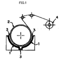
- a usual electrolytic copper foil is for example produced by an electrolytic foil manufacturing apparatus shown in FIG. 1 .
- the electrolytic foil manufacturing apparatus is comprised of a rotating drum shaped cathode 2 (surface made of SUS or titanium) and an anode 1 (lead or precious metal oxide-coated titanium electrode) arranged concentrically with the cathode 2.
- the electrolytic foil manufacturing apparatus is supplied with an electrolyte 3 while a current is run across the two electrodes so as to electrolytically deposit copper to a predetermined thickness on the surface of the cathode 2, then the copper is peeled off from the surface of the cathode 2 in the form of foil.
- the copper foil at this stage is sometimes called untreated electrolytic copper foil 4.
- the surface of the untreated electrolytic copper foil 4 which contacted the electrolyte is called as the "matte-side surface", while the surface which contacted the rotating drum-shaped cathode 2 is called the "shiny-side surface”.
- the copper foil may also be produced by an electrolytic foil manufacturing apparatus using a plate shaped cathode.
- the surface roughness of the electrolytic copper foil just after production is the surface roughness of the cathode transferred to it, so it is preferable to use a cathode whose surface roughness is Ra: 0.01 to 0.3 ⁇ m and Rz: 0.1 to 2.0 ⁇ m as the cathode for electrodeposition of copper.
- a cathode whose surface roughness is Ra: 0.01 to 0.3 ⁇ m and Rz: 0.1 to 2.0 ⁇ m as the cathode for electrodeposition of copper.
- the surface roughness of the matte side of the electrolytic copper foil is preferably an Ra of 0.01 to 0.2 ⁇ m and an Rz of 0.05 to 1.5 ⁇ m.
- a surface roughness of an Ra of less than 0.01 ⁇ m and/or an Rz of less than 0.05 ⁇ m is extremely difficult even if bright plating is performed. In practice, manufacture is close to impossible.
- the upper limit of the roughness is preferably made an Ra of less than 0.2 ⁇ m and an Rz of less than 1.5 ⁇ m.
- a surface roughness of the shiny side and/or the matte side of an Ra of less than 0.2 ⁇ m and an Rz of less than 1.0 ⁇ m is more preferable.
- the thickness of the electrolytic copper foil is preferably 3 ⁇ m to 70 ⁇ m. This is because manufacture of copper foil of a thickness of less than 3 ⁇ m is difficult due to handling technology etc. and is not practical.
- the upper limit of the thickness is about 70 ⁇ m from the viewpoint of the current state of use of circuit boards. This is because it is difficult to conceive of electrolytic copper foil of a thickness of 70 ⁇ m or more being used as copper foil for circuit boards. Further, there is no cost benefit to using electrolytic copper foil.
- the copper electrolyte for depositing the electrolytic copper foil there are a copper sulfate plating solution, copper pyrophosphate plating solution, copper sulfamate plating solution, etc. Considering costs etc., a copper sulfate plating solution is preferable.
- the copper sulfate plating solution preferably has a sulfuric acid concentration of 20 to 150 g/L, especially 30 to 100 g/L. If the sulfuric acid concentration is less than 20 g/L, the flow of current becomes harder, so practical operation becomes difficult. Further, the uniformity of plating and electrodeposition performance also become poorer. If the sulfuric acid concentration is more than 150 g/L, the copper solubility decreases, so a sufficient copper concentration can no longer be obtained and practical operation becomes difficult. Further, the corrosion of equipment is promoted.
- the copper concentration is preferably 40 to 150 g/L, especially 60 to 100 g/L. If the copper concentration becomes less than 40 g/L, it is difficult to secure the current density at which practical operation is possible in manufacturing electrolytic copper foil. A copper concentration of more than 150 g/L requires a considerably high temperature and therefore is impractical.
- the current density is preferably 20 to 200A/dm 2 , especially 30 to 120A/dm 2 . If the current density becomes less than 20A/dm 2 , in the manufacture of electrolytic copper foil, the production efficiency is extremely low, so this is impractical. A current density of more than 200A/dm 2 requires a considerably high copper concentration, high temperature, and high flow velocity, and the production equipment of the electrolytic copper foil is subjected to a high load, so this is impractical.
- the electrolytic bath temperature is preferably 25 to 80°C, especially 30 to 70°C. If the bath temperature becomes less than 25°C, in the manufacture of the electrolytic copper foil, it is difficult to secure a sufficient copper concentration and current density, so this is impractical. Further, a bath temperature of more than 80°C is extremely difficult in terms of operation and equipment, so this is impractical.
- the electrolyte has chlorine added to it if necessary.
- the chlorine concentration is preferably 1 to 100 ppm, especially 10 to 50 ppm. If the chlorine concentration becomes less than 1 ppm, it becomes difficult to obtain the effect of the later described additives. If more than 100 ppm, normal plating becomes difficult.
- the electrolysis conditions are suitably adjusted to conditions where problems such as deposition of copper and burning of plating do not occur within each range.
- a reaction product of at least one type of di- or poly-halogenated chain saturated aliphatic hydrocarbon compound, at least one type of di- or poly-halogenated chain saturated aliphatic hydrocarbon compound which has one or more ether bonds, or a combination of at least one type of di- or poly-halogenated chain saturated aliphatic hydrocarbon compound and at least one type of di- or poly-halogenated chain saturated aliphatic hydrocarbon compound which has one or more ether bonds with a heterocyclic compound which has two nitrogen atoms is added as a leveler.
- the number of carbon atoms of the di- or poly-halogenated chain saturated aliphatic hydrocarbon compound is in general 1 to 30, preferably 2 to 18, more preferably 4 to 8.
- the number of carbon atoms of the di- or poly-halogenated chain saturated aliphatic hydrocarbon compound which has one or more ether bonds is 4 to 30, preferably 4 to 12, more preferably 6 to 10.
- 2,2'-dichloroethyl ether, 1,2-bis(2-chloroethoxy)ethane, diethyleneglycol-bis(2-chloroethyl)ether, triethylene glycol-bis(2-chloroethyl)ether, 2,2'-dichloropropyl ether, 2,2'-dichlorobutyl ether, tetraethylene glycol-bis(2-bromoethyl)ether, heptaethylene glycol-bis(2-chloroethyl)ether, tridecaethylene glycol-bis (2-bromoethyl)ether, etc. can be mentioned. These compounds are used alone or in combinations of a plurality of types.
- heterocyclic compound which has two nitrogen atoms piperazine, triethylenediamine, 2-methylpiperazine, 2,6-dimethylpiperazine, 2,5-dimethylpiperazine, homopiperazine, 2-pyrazoline, imidazole, 2-methylimidazole, 2-ethylimidazole, 2-propylimidazole, 4-methylimidazole, histidine, 1-(3-aminopropyl)imidazole, 2-imidazoline, 3-imidazoline, 4-imidazoline, 2-methyl-2-imidazoline, pyrazole, 1-methylpyrazole, 3-methylpyrazole, 1,3-dimethylpyrazole, 1,4-dimethylpyrazole, 1,5-dimethylpyrazole, 3,5-dimethylpyrazole, benzimidazole, indazole, piperazine, 2-methylpiperazine, 2,5-dimethylpiperazine, pyrimidine, pyridazine, etc.
- 2-pyrazoline, pyrazole, imidazole, 2-methylimidazole, 2-imidazoline, 3-imidazoline, 4-imidazoline, 2-methyl-2-imidazoline, etc. are preferable.
- a reaction product of a combination of a di- or poly-halogenated chain saturated aliphatic hydrocarbon compound and a di- or poly-halogenated chain saturated aliphatic hydrocarbon compound which has one or more ether bonds with a heterocyclic compound which has two nitrogen atoms can be used.
- reaction product comprised of the above-mentioned starting material compound to which dimethylamine, diethanolamine, ethylenediamine, or another aliphatic amino compound, phenylenediamine or another aromatic amino compound, succinyl chloride, glutaryl chloride, fumaryl chloride, dichloroxylylene, phthaloyl chloride, or another compound which has a plurality of reactive groups is added and reacted as a third material can be used.
- use of epichlorohydrin or another epihalohydrin compound as the third reaction component is not preferable because the expected effect of the reaction product cannot be obtained.
- the reaction temperature for producing the reaction product of a di- or poly-halogenated chain saturated aliphatic hydrocarbon compound or di- or poly-halogenated chain saturated aliphatic hydrocarbon compound which has one or more ether bonds with a heterocyclic compound which has two nitrogen atoms is from room temperature to 200°C, preferably 50°C to 130°C.
- the reaction time for producing the reaction product of a di- or poly-halogenated chain saturated aliphatic hydrocarbon compound or di- or poly-halogenated chain saturated aliphatic hydrocarbon compound which has one or more ether bonds with a heterocyclic compound which has two nitrogen atoms is 1 hour to 100 hours, preferably 3 hours to 50 hours.
- the reaction for producing the above reaction product of a di- or poly-halogenated chain saturated aliphatic hydrocarbon compound or di- or poly-halogenated chain saturated aliphatic hydrocarbon compound which has one or more ether bonds with a heterocyclic compound which has two nitrogen atoms can be performed without a solvent, but a solvent may also be used.
- a solvent methanol, ethanol, 1-propanol, isopropanol, t-butanol, 1-butanol, and other alcohols, dimethylformamide, dioxane, tetrahydrofuran, methyl cellosolve, ethyl cellosolve, dimethyl cellosolve, diethyl cellosolve, etc. may be used.
- a halogen may be generated.
- this halogen may be contained, but preferably the halogen is removed by a well known method, for example, an ion exchange method, a method of insolubilizing it as alkaline metal halide by a reaction with an alkali metal hydroxide etc.
- the selection of whether the reaction product should be allowed to contain a halogen is made so as to satisfy the required performance as a copper electrolyte.
- the brightener which is used in the present embodiment, one may be suitably selected from known ones.
- 3-mercaptopropane sulfonic acid and its salt, bis(3-sulfopropyl)disulfide and its salt, N,N-dimethyldithiocarbamic acid (3-sulfopropyl)ester, N,N-dimethyldithiocarbamic acid (3-sulfoethyl)ester, sodium 3-(benzothiazolylthio)ethyl sulfonate, pyridiniumpropyl sulfobetaine, etc. can be mentioned.
- the polymer When adding a polymer to the copper electrolyte, the polymer may be suitably selected from known ones.
- a molecular weight 200 or greater polyethyleneglycol, polypropyleneglycol, copolymer of polyethyleneglycol and polypropyleneglycol, C1 to C6 alkyl monoether of the above three types of glycols, polyoxyethylene glyceryl ether, polyoxypropylene glyceryl ether, polyoxyethylene polyoxypropylene glyceryl ether, etc. can be mentioned.
- one of a molecular weight of 500 to 100,000 is preferable.
- the contents of elements taken in from the plating solution and additive ingredients such as chlorine (Cl), nitrogen (N), and sulfur (S) are preferably, in terms of intensity ratio with copper (Cu) in SIMS (secondary ion mass spectrometry) analysis of different parts in the copper foil depth direction, chlorine (Cl) of less than 0.5%, nitrogen (N) of less than 0.005%, and sulfur (S) of less than 0.005%.
- chlorine (Cl) of less than 0.5%
- sulfur (S) of less than 0.005%.
- the oxygen (O) is less than 1% and the carbon (C) less than 0.1%.
- the electrolytic copper foil of the present embodiment is an electrolytic copper foil in which there are few impurities as a whole and in which there are not many partially either (impurities are averagely distributed). Therefore, the electrolytic copper foil of the present embodiment, when subjected to the heat history in the circuit board fabrication process, especially a heat history that is equivalent to the heat history applied when bonding with a polyimide film, can be given flexibility and bendability equal to or better than those of rolled copper foil because the impurities are low and therefore grain coarsening progresses easily.
- the electrolytic copper foil produced as above when heat treated so that the LMP value shown in Equation 1 (hereinafter, simply described the "LMP value”) becomes 9000 or more, becomes an electrolytic copper foil which has a crystal distribution of 70% or more of crystal grains having a maximum length of the crystal grains after heat treatment of 10 ⁇ m or more.
- the heat treatment is performed so that a LMP value becomes 11,000 or more.
- LMP T + 273 * 20 + Logt where, 20 is the material constant of copper, T is the temperature (°C), and t is the time (hr).
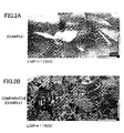
- FIG. 2 gives examples of electron micrographs of the cross-sectional surfaces of electrolytic copper foils, wherein FIG. 2A is a cross-sectional photograph of the electrolytic copper foil of this embodiment, and FIG. 2B is a cross-sectional photograph of a conventional electrolytic copper foil.
- the maximum length of the crystal grains is measured by the method of measuring the lengths of crystal grains in the long axis direction in a 1000 ⁇ m 2 area of a micrograph capturing a cross-section of the electrolytic copper foil, measuring the area occupied by crystal grains of a length of 10 ⁇ m or more, and calculating what percent the measured area is of the area of the cross-section as a whole.
- the 0.2% proof stress of the copper foil after the above heat treatment is preferably less than 10 kN/cm 2 , and the Young's modulus is preferably less than 2000 kN/cm 2 . Note that the 0.2% proof stress is optimally less than 8 kN/cm 2 .
- the present invention was explained with reference to an electrolytic copper foil, but it may also be a copper plating layer provided on a substrate in a printed circuit board or a copper plating layer provided on a metal wire. That is, a thick plating provided on a copper laminated substrate after etching, a thick plating provided on an organic film after forming a thin film by sputtering or non-electrolytic plating, and a copper plating layer provided on a metal plate or wire may also be formed by the copper electrolyte of the present invention. Note that, in many cases, a copper plating layer is formed on a metal thin film as explained above, so copper plating is generally performed at low current density conditions compared with electrolytic copper foil.
- the preferred ranges of copper concentration, current density, and electrolyte temperature differ from those of an electrolytic copper foil.
- the preferred range of copper concentration is 30 to 70 g/L
- the preferred range of current density is 0.1 to 15 A/dm 2
- the preferred range of electrolyte temperature is 20 to 50°C.
- the hardness becomes a problem.
- the Vickers hardness is preferably less than 60Hv.
- Table 1 shows the electrolyte composition.
- a copper sulfate plating solution of each composition shown in Table 1 (below, sometimes referred to as an "electrolyte") was run through an activated charcoal filter to purify it, then the additives shown in Table 2 were added to predetermined concentrations.
- an 18 ⁇ m thick electrolytic copper foil was deposited on a rotating drum made of titanium shown in FIG. 1 from the copper sulfate plating solution by the current density shown in Table 1, then was peeled off and rolled up.
- the produced electrolytic copper foil and copper plating layer were respectively divided into three samples. Among these, one sample each was used to measure the amounts of impurity elements contained inside the electrolytic copper foil and the copper plating layer and the surface roughness. Further, another unused sample of each was heat-treated and observed for crystal grains at the cross-section. Furthermore, a sample of the electrolytic copper foil was tested for tensile strength, while a sample of the copper plating layer was tested for Vickers hardness. Finally, for each remaining unused sample, the sample of the electrolytic copper foil was hot pressed with a polyimide film, then the sample of the copper plating layer was heat-treated by the same temperature setting, then these samples were tested by an IPC bending test. The details of each measurement and examination are described below.
- the amounts of impurity elements inside the electrolytic copper foils and copper plating layers of Examples 1 to 7, Examples 14 to 20, Comparative Examples 1 to 3, and Comparative Examples 7 to 9 were measured in the depth direction using SIMS analysis.
- the measured elements were oxygen (O), carbon (C), chlorine (Cl), nitrogen (N), and sulfur (S).
- the measurement conditions of the SIMS analysis were as follows.
- the surfaces of the electrolytic copper foils and copper plating layers are affected by dirt and oxide layers, so the portions from the surfaces to 2 ⁇ m down in the depth direction were removed by sputtering, then the measurement was started and the portion down to a depth of 4 ⁇ m was analyzed.
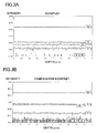
- the intensity ratio was calculated from the average value of the intensity of each measured element and the average value of the intensity of copper. Examples of the measurement results of the SIMS analysis are shown in FIG. 3A and FIG. 3B , while the calculation results of the intensity ratio are shown in Table 3.
- the surface roughnesses Ra and Rz of the electrolytic copper foils and the copper plating layers of Examples 1 to 7, Examples 14 to 20, Comparative Examples 1 to 3, and Comparative Examples 7 to 9 were measured using a contact type surface roughness gauge.
- the surface roughness is shown by Ra (arithmetic average roughness) and Rz (ten-point average roughness) defined in JIS-B-0601 (Japanese Industrial Standard).
- the reference length is 0.8 mm.
- the electrolytic copper foils were measured for the Ra and Rz of the matte-side surfaces and shiny-side surfaces and the copper plating layers were measured for the Ra and Rz of the surfaces of the copper plating layers and the non-electrolytic copper layer surfaces before plating. The results of surface roughness measurement are described in Table 3.
- the electrolytic copper foils of Examples 1 to 13 and Comparative Examples 1 to 6 were heat-treated under the above heat conditions, the foils were cut into 6 inch (length) x 0.5 inch (width) test pieces which were then measured for 0.2% proof stress and Young's modulus using a tensile tester. Further, the tension rate was 50 mm/min. The results of the tensile test are described in Table 4.
- the 0.2% proof stress is the value obtained in the curve of the relationship of strain and stress by drawing a tangent to the curve at the point of 0% strain, drawing a line parallel to that tangent at the point of 0.2% strain, and dividing the stress at the point where that line and the curve intersect by the cross-sectional area.
- the electrolytic plating layers of Examples 14 to 26 and Comparative Examples 7 to 12 were heat-treated under the above heating conditions, then the copper plating layers were embedded in a resin, the cross-sections were cut, then the cross-sections were polished and a Vickers hardness tester was used to measure the Vickers hardness. Further, the load was 10 gf and load holding time was 15 sec. The results of the Vickers hardness test are described in Table 4.
- the obtained electrolytic copper foils to which the polyimide films were bonded and the copper plating layers were etched with the circuit patterns shown in FIG. 4A , then, as shown in FIG.
- the obtained test samples were tested by IPC flex tests under the following conditions, then the rate of increase of the electrical resistance from an initial state was measured.
- the results of the IPC flex test are described in Table 5.
- Table 3 The measurement results are shown in Table 3, Table 4, and Table 5.
- Table 3 Strength ratio against copper in SIMS analysis (%) Surface roughness Matte-side surface of electrolytic copper foil or surface of copper plating layer Shiny-side surface of electrolytic copper foil or surface of non-electrolytic copper plating layer Cl N S O C Ra ( ⁇ m) Rz ( ⁇ m) Ra ( ⁇ m) Rz ( ⁇ m) Ex. 1 0.24 0 0 0.53 0.07 0.13 0.55 0.21 1.65 Ex. 2 0.21 0 0.002 0.42 0.06 0.11 0.45 0.23 1.55 Ex. 3 0.15 0 0 0.55 0.06 0.10 0.50 0.20 1.50 Ex. 4 0.16 0 0 0.49 0.06 0.12 0.55 0.23 1.45 Ex.
- the percentage of the crystal grains of a length of 10 ⁇ m or more (crystal distribution) is 70% or more.
- the 0.2% proof stresses of the electrolytic copper foils were less than 10 kN/cm 2
- the Young's moduli were less than 2000 kN/cm 2 .
- the Vickers hardness of the copper plating layers was less than 60Hv.
- the 0.2% proof stresses of the electrolytic copper foils were 10 kN/cm 2 or more or the Young's moduli were 2000kN/cm 2 or more.
- the Vickers hardness of the copper plating layers was 60Hv or more. These did not satisfy all of the conditions of the present invention.
- the electrolytic copper foils and the copper plating layers showed poor flexing characteristics as compared with the examples.
- the 0.2% proof stresses of the electrolytic copper foils were 10 kN/cm 2 or more or the Young's moduli were 2000kN/cm 2 or more.
- the electrolytic copper coating, the method of manufacturing the same, and the copper electrolyte for manufacturing an electrolytic copper coating of the present invention can be applied to a copper plating layer provided on a substrate in a printed circuit board, a multilayer printed circuit board, and a chip-on-film circuit board, a copper plating layer provided on a metal wire, or an electrolytic copper foil.
Landscapes
- Chemical & Material Sciences (AREA)
- Engineering & Computer Science (AREA)
- Chemical Kinetics & Catalysis (AREA)
- Electrochemistry (AREA)
- Materials Engineering (AREA)
- Metallurgy (AREA)
- Organic Chemistry (AREA)
- Microelectronics & Electronic Packaging (AREA)
- Electroplating And Plating Baths Therefor (AREA)
- Electroplating Methods And Accessories (AREA)
Applications Claiming Priority (2)
| Application Number | Priority Date | Filing Date | Title |
|---|---|---|---|
| JP2008154025 | 2008-06-12 | ||
| PCT/JP2009/060792 WO2009151124A1 (fr) | 2008-06-12 | 2009-06-12 | Revêtement électrolytique de cuivre et son procédé de fabrication, et électrolyte de cuivre pour la fabrication de revêtements électrolytiques de cuivre |
Publications (2)
| Publication Number | Publication Date |
|---|---|
| EP2302103A1 true EP2302103A1 (fr) | 2011-03-30 |
| EP2302103A4 EP2302103A4 (fr) | 2014-05-28 |
Family
ID=41416826
Family Applications (1)
| Application Number | Title | Priority Date | Filing Date |
|---|---|---|---|
| EP09762554.5A Withdrawn EP2302103A4 (fr) | 2008-06-12 | 2009-06-12 | Revêtement électrolytique de cuivre et son procédé de fabrication, et électrolyte de cuivre pour la fabrication de revêtements électrolytiques de cuivre |
Country Status (6)
| Country | Link |
|---|---|
| US (1) | US20110139626A1 (fr) |
| EP (1) | EP2302103A4 (fr) |
| JP (1) | JP2010018885A (fr) |
| KR (1) | KR101274544B1 (fr) |
| CN (1) | CN102105622A (fr) |
| WO (1) | WO2009151124A1 (fr) |
Cited By (3)
| Publication number | Priority date | Publication date | Assignee | Title |
|---|---|---|---|---|
| KR20130021344A (ko) * | 2011-08-22 | 2013-03-05 | 롬 앤드 하스 일렉트로닉 머트어리얼즈, 엘.엘.씨. | 도금 배스 및 방법 |
| EP2312020A4 (fr) * | 2008-07-07 | 2014-05-28 | Furukawa Electric Co Ltd | Feuille de cuivre électrolytique et stratifié revêtu de cuivre |
| US20160076160A1 (en) * | 2014-09-15 | 2016-03-17 | Enthone Inc. | Levelers for copper deposition in microelectronics |
Families Citing this family (26)
| Publication number | Priority date | Publication date | Assignee | Title |
|---|---|---|---|---|
| US8268157B2 (en) * | 2010-03-15 | 2012-09-18 | Rohm And Haas Electronic Materials Llc | Plating bath and method |
| WO2012016160A2 (fr) * | 2010-07-30 | 2012-02-02 | University Of Utah Research Foundation | Films nanostructurés et procédés associés |
| JP5276158B2 (ja) | 2010-12-27 | 2013-08-28 | 古河電気工業株式会社 | リチウムイオン二次電池、該電池用負極電極、該電池負極集電体用電解銅箔 |
| JP5794806B2 (ja) * | 2011-03-30 | 2015-10-14 | 古河電気工業株式会社 | 表面処理銅箔、および、該表面処理銅箔を用いた銅張積層基板、並びにプリント配線基板 |
| JP5730742B2 (ja) * | 2011-10-25 | 2015-06-10 | 古河電気工業株式会社 | リチウムイオン二次電池用電解銅箔とその製造方法 |
| CN103074646A (zh) * | 2013-01-11 | 2013-05-01 | 安徽铜冠铜箔有限公司 | 一种钛辊表面铜箔收卷方式 |
| JP6212273B2 (ja) * | 2013-03-29 | 2017-10-11 | Jx金属株式会社 | 電解銅箔、それを用いた銅張積層体及びその製造方法、プリント配線板及びその製造方法、及び電子部品及びその製造方法 |
| TWI539032B (zh) * | 2013-08-01 | 2016-06-21 | Chang Chun Petrochemical Co | Electrolytic copper foil, cleaning fluid composition and cleaning copper foil method |
| JP5810197B2 (ja) * | 2013-09-11 | 2015-11-11 | 古河電気工業株式会社 | 電解銅箔、フレキシブル配線板及び電池 |
| US9403762B2 (en) | 2013-11-21 | 2016-08-02 | Rohm And Haas Electronic Materials Llc | Reaction products of guanidine compounds or salts thereof, polyepoxides and polyhalogens |
| JP6260860B2 (ja) * | 2013-12-27 | 2018-01-17 | 日立金属株式会社 | 電解アルミニウム箔、それを用いた電池用電極、及び蓄電デバイス、並びに電解アルミニウム箔の製造方法 |
| JP6421719B2 (ja) * | 2015-07-31 | 2018-11-14 | 住友金属鉱山株式会社 | フレキシブル配線板用の電気銅めっき液及び該電気銅めっき液により製造される積層体の製造方法 |
| CN105483764B (zh) * | 2015-12-04 | 2019-02-22 | 广东嘉元科技股份有限公司 | 一种电解铜箔添加剂 |
| US10749278B2 (en) * | 2016-01-15 | 2020-08-18 | Taiwan Semiconductor Manufacturing Co., Ltd. | Method of electroplating metal into recessed feature and electroplating layer in recessed feature |
| JP6834070B2 (ja) * | 2016-06-13 | 2021-02-24 | 石原ケミカル株式会社 | 電気スズ及びスズ合金メッキ浴、当該メッキ浴を用いて電着物を形成した電子部品の製造方法 |
| TW201900939A (zh) * | 2017-05-09 | 2019-01-01 | 日商Jx金屬股份有限公司 | 電解銅箔、覆銅積層板、印刷配線板及其製造方法、以及電子機器及其製造方法 |
| WO2018207788A1 (fr) * | 2017-05-09 | 2018-11-15 | Jx金属株式会社 | Feuille de cuivre électrolytique, son procédé de production, stratifié cuivré, carte de circuit imprimé, son procédé de production, dispositif électronique et son procédé de production |
| WO2018207785A1 (fr) * | 2017-05-09 | 2018-11-15 | Jx金属株式会社 | Feuille de cuivre électrolytique et son procédé de production, stratifié cuivré, carte de circuit imprimé et son procédé de production, dispositif électronique et son procédé de production |
| CN109601024A (zh) * | 2017-07-31 | 2019-04-09 | 卢森堡电路箔片股份有限公司 | 表面处理过的铜箔和覆铜箔层压板 |
| KR102302184B1 (ko) * | 2018-02-01 | 2021-09-13 | 에스케이넥실리스 주식회사 | 고온 치수 안정성 및 집합조직 안정성을 갖는 전해동박 및 그 제조방법 |
| TWI705160B (zh) | 2019-12-09 | 2020-09-21 | 長春石油化學股份有限公司 | 電解銅箔、包含其的電極和覆銅積層板 |
| TWI715424B (zh) * | 2020-01-22 | 2021-01-01 | 長春石油化學股份有限公司 | 電解銅箔、電極及包含其之鋰離子電池 |
| CN114073170B (zh) * | 2020-04-01 | 2025-01-03 | 住友电气工业株式会社 | 柔性印刷布线板及其制造方法 |
| JP2023154854A (ja) * | 2022-04-08 | 2023-10-20 | 日本電解株式会社 | 電解銅箔およびその製造方法 |
| WO2024016330A1 (fr) * | 2022-07-22 | 2024-01-25 | 扬州纳力新材料科技有限公司 | Raffineur de grains de placage de cuivre exempt de cyanure, solution de placage de cuivre exempt de cyanure, procédé de préparation associé et application correspondante |
| CN115287715B (zh) * | 2022-08-25 | 2023-06-23 | 广东盈华电子科技有限公司 | 一种中抗拉强度锂电池用双光铜箔的生产工艺 |
Family Cites Families (13)
| Publication number | Priority date | Publication date | Assignee | Title |
|---|---|---|---|---|
| JPS527819A (en) * | 1975-07-10 | 1977-01-21 | Furukawa Electric Co Ltd:The | Process for smooth electrodeposition of copper |
| US4038161A (en) * | 1976-03-05 | 1977-07-26 | R. O. Hull & Company, Inc. | Acid copper plating and additive composition therefor |
| LU90532B1 (en) * | 2000-02-24 | 2001-08-27 | Circuit Foil Luxembourg Trading Sarl | Comosite copper foil and manufacturing method thereof |
| JP3520034B2 (ja) * | 2000-07-25 | 2004-04-19 | 古河電気工業株式会社 | 電子電気機器部品用銅合金材 |
| KR20030094098A (ko) * | 2002-06-03 | 2003-12-11 | 쉬플리 캄파니, 엘.엘.씨. | 평탄화제 화합물 |
| JP3756852B2 (ja) * | 2002-07-01 | 2006-03-15 | 日本電解株式会社 | 電解銅箔の製造方法 |
| US6878458B2 (en) * | 2002-09-12 | 2005-04-12 | Matsushita Electric Industrial Co., Ltd. | Metal foil for current collector of secondary battery and method of producing the same |
| JP4083171B2 (ja) * | 2002-12-25 | 2008-04-30 | 日鉱金属株式会社 | 特定骨格を有する四級アミン化合物重合体及び有機硫黄化合物を添加剤として含む銅電解液並びにそれにより製造される電解銅箔 |
| TW200613586A (en) * | 2004-07-22 | 2006-05-01 | Rohm & Haas Elect Mat | Leveler compounds |
| JP4973829B2 (ja) * | 2004-07-23 | 2012-07-11 | 上村工業株式会社 | 電気銅めっき浴及び電気銅めっき方法 |
| JP2007146289A (ja) * | 2005-10-31 | 2007-06-14 | Mitsui Mining & Smelting Co Ltd | 電解銅箔の製造方法、該製造方法で得られる電解銅箔、該電解銅箔を用いて得られる表面処理銅箔及び該電解銅箔又は該表面処理銅箔を用いて得られる銅張積層板 |
| JP4712759B2 (ja) * | 2006-06-07 | 2011-06-29 | 古河電気工業株式会社 | 表面処理電解銅箔及びその製造方法、並びに回路基板 |
| MY158819A (en) * | 2007-04-20 | 2016-11-15 | Jx Nippon Mining & Metals Corp | Electrolytic copper foil for lithium rechargeable battery and process for producing the copper foil |
-
2009
- 2009-06-12 KR KR1020117000332A patent/KR101274544B1/ko active Active
- 2009-06-12 CN CN2009801302754A patent/CN102105622A/zh active Pending
- 2009-06-12 EP EP09762554.5A patent/EP2302103A4/fr not_active Withdrawn
- 2009-06-12 WO PCT/JP2009/060792 patent/WO2009151124A1/fr not_active Ceased
- 2009-06-12 JP JP2009141216A patent/JP2010018885A/ja active Pending
- 2009-06-12 US US12/997,420 patent/US20110139626A1/en not_active Abandoned
Cited By (7)
| Publication number | Priority date | Publication date | Assignee | Title |
|---|---|---|---|---|
| EP2312020A4 (fr) * | 2008-07-07 | 2014-05-28 | Furukawa Electric Co Ltd | Feuille de cuivre électrolytique et stratifié revêtu de cuivre |
| KR20130021344A (ko) * | 2011-08-22 | 2013-03-05 | 롬 앤드 하스 일렉트로닉 머트어리얼즈, 엘.엘.씨. | 도금 배스 및 방법 |
| JP2013049922A (ja) * | 2011-08-22 | 2013-03-14 | Rohm & Haas Electronic Materials Llc | めっき浴および方法 |
| EP2562294A3 (fr) * | 2011-08-22 | 2017-04-12 | Rohm and Haas Electronic Materials LLC | Appareil et bain de placage |
| US20160076160A1 (en) * | 2014-09-15 | 2016-03-17 | Enthone Inc. | Levelers for copper deposition in microelectronics |
| EP3195708A4 (fr) * | 2014-09-15 | 2018-07-18 | Macdermid Enthone Inc. | Agents égalisants pour dépôt de cuivre en micro-électronique |
| US10294574B2 (en) | 2014-09-15 | 2019-05-21 | Macdermid Enthone Inc. | Levelers for copper deposition in microelectronics |
Also Published As
| Publication number | Publication date |
|---|---|
| KR101274544B1 (ko) | 2013-06-17 |
| CN102105622A (zh) | 2011-06-22 |
| EP2302103A4 (fr) | 2014-05-28 |
| US20110139626A1 (en) | 2011-06-16 |
| KR20110017429A (ko) | 2011-02-21 |
| WO2009151124A1 (fr) | 2009-12-17 |
| JP2010018885A (ja) | 2010-01-28 |
Similar Documents
| Publication | Publication Date | Title |
|---|---|---|
| EP2302103A1 (fr) | Revêtement électrolytique de cuivre et son procédé de fabrication, et électrolyte de cuivre pour la fabrication de revêtements électrolytiques de cuivre | |
| CN102124148B (zh) | 电沉积铜箔和覆铜层合板 | |
| JP3058445B2 (ja) | 特性の調整された、印刷回路基板用の電着された箔並びにそれを製造するための方法及び電解槽溶液 | |
| US6231742B1 (en) | Electrolytic Copper foil and process for producing the same | |
| US8153273B2 (en) | Surface treated electrodeposited copper foil and circuit board | |
| KR101154203B1 (ko) | 전해 동박, 그 전해 동박을 이용한 표면 처리 동박 및 그 표면 처리 동박을 이용한 동박 적층판 및 그 전해 동박의 제조 방법 | |
| JP5391366B2 (ja) | 電解銅箔、該電解銅箔を使用した配線板及びフレキシブル配線板 | |
| JP5255229B2 (ja) | 電解銅箔、その電解銅箔を用いた表面処理銅箔及びその表面処理銅箔を用いた銅張積層板並びにその電解銅箔の製造方法 | |
| US10190225B2 (en) | Electrodeposited copper foil with low repulsive force | |
| JPH0754183A (ja) | 電着銅箔、および、塩化物イオンならびに有機添加剤の制御添加物を含有する電解質溶液を用いる電着銅箔の製造方法 | |
| US20120031648A1 (en) | Wiring circuit board | |
| KR100454270B1 (ko) | 저조도 전해동박의 제조방법 및 전해동박 | |
| KR20230129209A (ko) | 표면처리 전해동박, 이의 제조방법, 및 이의 용도 | |
| KR100694382B1 (ko) | 고강도를 갖는 저조도 전해동박의 제조방법, 이 방법에의해 제조된 전해동박, 및 이 전해동박을 사용하여 제작한전자 부품 | |
| EP4202084A2 (fr) | Feuille de cuivre électrolytique à double couche et son procédé de fabrication | |
| TWI465609B (zh) | An electrolytic copper film, a method for producing the same, and a copper electrolytic solution for manufacturing a copper electrolytic film | |
| TWI396779B (zh) | Copper foil and its manufacturing method, and flexible printed circuit board | |
| KR20180109364A (ko) | 양호한 내굴곡성을 갖는 연성동박적층판 및 연성동박적층판의 시험 방법 | |
| KR102392049B1 (ko) | 양호한 방청 성능을 갖는 연성동박적층판 및 연성동박적층판의 시험 방법 | |
| KR20160076964A (ko) | 전해 동박, 그리고 이를 포함하는 fccl 및 ccl | |
| EP4446476A1 (fr) | Feuille de cuivre électrolytique présentant des caractéristiques de résistance et d'allongement élevées | |
| KR102567549B1 (ko) | 전해 동박 및 이를 포함하는 이차전지 | |
| KR20180113805A (ko) | 양호한 방청 성능을 갖는 연성동박적층판 및 연성동박적층판의 시험 방법 | |
| KR102432584B1 (ko) | 비전도성 고분자막과의 박리강도를 향상시킬 수 있는 동박, 그 제조방법, 및 그것을 포함하는 연성동박적층필름 |
Legal Events
| Date | Code | Title | Description |
|---|---|---|---|
| PUAI | Public reference made under article 153(3) epc to a published international application that has entered the european phase |
Free format text: ORIGINAL CODE: 0009012 |
|
| 17P | Request for examination filed |
Effective date: 20110112 |
|
| AK | Designated contracting states |
Kind code of ref document: A1 Designated state(s): AT BE BG CH CY CZ DE DK EE ES FI FR GB GR HR HU IE IS IT LI LT LU LV MC MK MT NL NO PL PT RO SE SI SK TR |
|
| AX | Request for extension of the european patent |
Extension state: AL BA RS |
|
| DAX | Request for extension of the european patent (deleted) | ||
| A4 | Supplementary search report drawn up and despatched |
Effective date: 20140428 |
|
| RIC1 | Information provided on ipc code assigned before grant |
Ipc: C25D 3/38 20060101ALI20140422BHEP Ipc: C25D 1/04 20060101AFI20140422BHEP Ipc: C25D 7/06 20060101ALI20140422BHEP Ipc: H05K 1/09 20060101ALI20140422BHEP Ipc: C25D 5/50 20060101ALI20140422BHEP Ipc: H05K 1/03 20060101ALN20140422BHEP |
|
| STAA | Information on the status of an ep patent application or granted ep patent |
Free format text: STATUS: THE APPLICATION IS DEEMED TO BE WITHDRAWN |
|
| 18D | Application deemed to be withdrawn |
Effective date: 20141126 |