EP2302341B1 - Detektionsschaltung mit verbessertem Blendschutz - Google Patents
Detektionsschaltung mit verbessertem Blendschutz Download PDFInfo
- Publication number
- EP2302341B1 EP2302341B1 EP10354047.2A EP10354047A EP2302341B1 EP 2302341 B1 EP2302341 B1 EP 2302341B1 EP 10354047 A EP10354047 A EP 10354047A EP 2302341 B1 EP2302341 B1 EP 2302341B1
- Authority
- EP
- European Patent Office
- Prior art keywords
- voltage
- amplifier
- circuit
- input
- output
- Prior art date
- Legal status (The legal status is an assumption and is not a legal conclusion. Google has not performed a legal analysis and makes no representation as to the accuracy of the status listed.)
- Active
Links
- 238000001514 detection method Methods 0.000 title claims description 22
- 239000003990 capacitor Substances 0.000 claims description 52
- 230000010354 integration Effects 0.000 claims description 13
- 238000000034 method Methods 0.000 claims description 5
- 230000005669 field effect Effects 0.000 claims description 4
- 230000005855 radiation Effects 0.000 claims description 3
- 239000000758 substrate Substances 0.000 description 11
- 230000028161 membrane depolarization Effects 0.000 description 7
- 238000004519 manufacturing process Methods 0.000 description 5
- 238000005286 illumination Methods 0.000 description 4
- 230000007423 decrease Effects 0.000 description 3
- 230000004313 glare Effects 0.000 description 3
- 239000006185 dispersion Substances 0.000 description 2
- 230000000694 effects Effects 0.000 description 2
- 235000021183 entrée Nutrition 0.000 description 2
- 238000005259 measurement Methods 0.000 description 2
- 230000015572 biosynthetic process Effects 0.000 description 1
- 230000004048 modification Effects 0.000 description 1
- 238000012986 modification Methods 0.000 description 1
- 230000010287 polarization Effects 0.000 description 1
- 230000000717 retained effect Effects 0.000 description 1
- 238000005303 weighing Methods 0.000 description 1
Images



Classifications
-
- G—PHYSICS
- G01—MEASURING; TESTING
- G01J—MEASUREMENT OF INTENSITY, VELOCITY, SPECTRAL CONTENT, POLARISATION, PHASE OR PULSE CHARACTERISTICS OF INFRARED, VISIBLE OR ULTRAVIOLET LIGHT; COLORIMETRY; RADIATION PYROMETRY
- G01J1/00—Photometry, e.g. photographic exposure meter
- G01J1/42—Photometry, e.g. photographic exposure meter using electric radiation detectors
- G01J1/44—Electric circuits
- G01J1/46—Electric circuits using a capacitor
-
- H—ELECTRICITY
- H04—ELECTRIC COMMUNICATION TECHNIQUE
- H04N—PICTORIAL COMMUNICATION, e.g. TELEVISION
- H04N25/00—Circuitry of solid-state image sensors [SSIS]; Control thereof
- H04N25/60—Noise processing, e.g. detecting, correcting, reducing or removing noise
- H04N25/62—Detection or reduction of noise due to excess charges produced by the exposure, e.g. smear, blooming, ghost image, crosstalk or leakage between pixels
- H04N25/621—Detection or reduction of noise due to excess charges produced by the exposure, e.g. smear, blooming, ghost image, crosstalk or leakage between pixels for the control of blooming
Definitions
- the invention also relates to a method for reading the radiation from a detection circuit.
- a photodiode 1 reverse biased, delivers a current representative of an observed scene.
- the photodiode 1 delivers this current, for a predefined duration, to an integrator device 2.
- the integrator device 2 is constituted by a capacitive transimpedance amplifier which comprises an amplifier 3 connected to a capacitor 4.
- the cathode of the photodiode 1 is connected to a first input of the amplifier 3 and a substrate potential V Sub is applied to it.
- 'anode of photodiode 1. As long as the potential of the first input of amplifier 3 is greater than the substrate potential V Sub , the diode is reverse biased and operates as expected.
- the current emitted by the photodiode 1 is then integrated by the capacitor 4 and the integrator 2 delivers at output a voltage V S which is representative of the illumination of the scene observed via the capacitor 4.
- V S which is representative of the illumination of the scene observed via the capacitor 4.
- the difference in potentials which exists at the terminals of the capacitor 4 modifies the potential V E of the first input of the amplifier 3 and therefore the polarization of the photodiode 1.
- the difference in potentials at the terminals of the photodiode 1 changes so that the photodiode becomes depolarized.
- This depolarization causes a modification, an increase, of the photon collection surface in the adjacent photodiodes.
- a photodiode is too bright, there is a dazzling effect on the adjacent photodiodes which deliver a current representative of an illumination greater than reality.
- an nMOS type transistor is connected between the first input and the output of the amplifier.
- the nMOS type transistor is connected, in parallel, to the terminals of the capacitor.
- the purpose of this transistor is to avoid depolarization of the photodiode by preventing the potential V E of the first input of the amplifier from falling below a limit value.
- An anti-glare voltage V AB is therefore applied to the gate electrode so that the transistor turns on before the photodiode is depolarized.
- the anti-glare voltage V AB is chosen so that the + photodiode is always reverse biased, that is to say that it is not reverse biased. direct.
- the anti-glare voltage V AB is defined with respect to the potential V E of the first input of the amplifier.
- the amplifier supplies this current through the capacitor, while maintaining the first input of the amplifier at the voltage value imposed on the second input.
- This charge of the capacitor results in an increase in the output voltage V S of the amplifier.
- the potential V E present at the first input of the amplifier, decreases. This decrease takes place until the potential difference between the gate electrode V AB and the first input of the amplifier reaches the threshold voltage of the transistor. Once this threshold voltage has been reached, the transistor turns on, the additional charges are evacuated and the potential V E of the first input of the amplifier no longer changes.
- the potential V E of the first input reaches a certain predefined threshold, the nMOS transistor turns on and the additional charges are discharged. The potential V E of the first input can therefore no longer evolve beyond a limit potential.
- the object of the invention is a detection circuit which corrects the dazzling phenomena and which is easy to implement while ensuring a reliable and repeatable production for industrial integration.
- the subject of the invention is also a method for protecting the detection circuit which is easy to implement while ensuring a reliable and repeatable implementation for industrial integration.
- the device according to the invention is defined in claim 1.
- the transistor 5 of the nMOS type connected, in parallel, to the terminals of the capacitor 4 must prevent a dazzling phenomenon from appearing on the adjacent photodiodes. It The transistor 5 must therefore avoid the depolarization of the photodiode 1, but it must not either prevent the capacitor 4 from storing a minimum of charges necessary for the primary purpose of the detection circuit, to define the illumination of the observed scene. It follows from these two conditions that the anti-glare potential V AB applied to the gate electrode of the nMOS type transistor 5 must be within a precise range.
- the anti-glare potential V AB applied to the gate electrode of the nMOS type transistor 5 must be lower than the reference potential V REF applied to the second input of the amplifier 3 to which is added the threshold voltage V th of transistor 5.
- the nMOS type transistor 5 is not in permanent conduction, because the potential V E of the first input of the amplifier 3 cannot be greater than V REF .
- the anti-glare potential V AB applied to the gate electrode of the nMOS type transistor 5 must also be greater than the potential of the substrate V Sub which is applied to the anode of the photodiode 1 to which are added the threshold voltage of the transistor V th and the minimum voltage V Dmin for which there is still reverse biasing of the photodiode 1. If the anti-glare potential V AB is lower than this limit potential, this means that the potential V E of the first input of amplifier 3 is less than the substrate potential V Sub to which is added the minimum bias voltage V Dmin . As a result, the difference in potentials at the terminals of photodiode 1 is less than the minimum bias voltage V Dmin and there is therefore depolarization of photodiode 1.
- the range of potentials V AB which must be imposed on the gate electrode to avoid the phenomenon of dazzling is of the order of 30 mV.
- the reference voltage is equal to 1.1V
- the substrate potential V Sub is equal to 1.05V
- the threshold voltage V th is of the order of 850mV
- the minimum bias voltage V Dmin is of the order of 20mV.
- the threshold voltage must be between 1.92 and 1.95V.
- the range of potentials authorized for the anti-glare voltage V AB is therefore very narrow to ensure proper operation of the circuit.
- This adjustment range typically corresponds to the dispersion which is observed, in the usual way, on the threshold voltage V th of the nMOS transistors.
- the dispersion of the cold threshold voltage is of the order of 15 mV at one sigma.
- the detection circuit has therefore been modified in order to make it more robust with respect to the vagaries of its production process.
- the detection circuit has, however, retained a reduced surface area and ease of integration which are elements necessary for its use in many fields of activity.
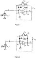
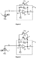
- the detection circuit comprises a photodiode 1 which is connected to an integrator device 2.
- the integrator device 2 comprises a transimpedance amplifier 3.
- the photodiode 1 is connected to a first input of the transimpedance amplifier 3.
- a reference voltage V REF is applied to a second input of the transimpedance amplifier.
- the detection circuit comprises a photodiode associated with a read circuit.
- the transimpedance amplifier used can be of the resistive type ( figure 3 ) or capacitive ( figure 4 ).
- the remainder of the description deals with a capacitive transimpedance amplifier but a resistive transimpedance amplifier can be substituted for it.
- the cases where a resistive transimpedance amplifier is used are not covered by the claims.
- the resistive transimpedance amplifier shown in figure 3 comprises an amplifier 3, typically an operational amplifier, and a resistor 6.
- the resistor 6 is connected between the first input and the output of the amplifier 3.
- a first electrical node E is defined by the connection of the photodiode 1 with the resistor 6 and the first input of the resistive transimpedance amplifier.
- a second electrical node S is defined by the connection of resistor 6 and the output of the resistive transimpedance amplifier.
- the capacitive transimpedance amplifier illustrated in figures 4 to 6 comprises an amplifier 3, typically an operational amplifier, and a capacitor 4.
- the capacitor 4 is connected between the first input and the output of the amplifier 3.
- a first electrical node E is defined by the connection of the photodiode 1 with the capacitor 4 and the first input of the capacitive transimpedance amplifier.
- a second electrical node S is defined by the connection of the capacitor 4 and the output of the capacitive transimpedance amplifier.
- a substrate potential V Sub is applied to a first terminal of photodiode 1 while the second terminal is connected to the first input of amplifier 3.
- the potential of the second terminal of photodiode 1 is therefore equal to the potential of first input of amplifier 3, i.e. at the potential V E of the first electrical node E.
- Photodiode 1 is therefore biased between the substrate potential V Sub and the potential V E of the first input of amplifier 3.
- the photodiode 1 is reverse biased to provide a current representative of the illumination of the observed scene, the substrate potentials V Sub and the first input V E of amplifier 3 are chosen accordingly.
- the read circuit also includes an anti-glare circuit and advantageously a reset circuit. Both the reset circuit and the anti-glare circuit are connected between the first input and the output of the capacitive transimpedance amplifier. They are therefore connected to the terminals of the capacitor 4 and therefore to the electrical nodes E and S.
- the read circuit comprises means 7 for comparing the output voltage V S of the transimpedance amplifier 3 with a reference voltage V AB . It also comprises means 8 for applying a feedback current to the first input E of the transimpedance amplifier when the difference between the output voltage V S and the setpoint voltage V AB reaches a threshold, c ' ie a limit value which cannot be exceeded.
- the read circuit may include a bias terminal which makes it possible to define the setpoint voltage. This bias terminal is separate from the amplifier input terminals.
- the anti-glare circuit comprises a field effect transistor 5 connected between the first input and the output of the transimpedance amplifier 3, here a capacitive transimpedance amplifier.
- the transistor 5 is therefore connected, in parallel, to the terminals of the capacitor 4.
- the transistor 5 is connected to the amplifier 3 in negative feedback.
- the reset circuit can also include a second transistor 9 connected between the first input and the output of the capacitive transimpedance amplifier.
- the second transistor 9 is therefore connected, in parallel, to the terminals of the capacitor 4.
- the second transistor 9 is connected to the amplifier 3 in negative feedback.
- the transistor 5 of the anti-glare circuit connected to the terminals of the capacitor 4 or of the resistor 6, is of the pMOS type.
- the substrate potential V Sub is applied to the anode of photodiode 1 while the cathode is connected to the first input of the capacitive transimpedance amplifier.
- the transistor 5 is therefore connected by its drain terminal to the cathode of the photodiode 1, typically at the level of the first input of the capacitive transimpedance amplifier, that is to say of the node E.
- the photodiode 1 being polarized in Conversely, the potential V E at node E is greater than the substrate potential V Sub .
- the transistor 5 being of the pMOS type, its on or off state is defined with respect to the potential difference which exists between the gate electrode and the output S of the amplifier 3.
- the potential of anti-glare V AB applied to the gate electrode of transistor 5 of pMOS type is defined with respect to the output of the capacitive transimpedance amplifier and no longer with respect to the first input as in the case of the nMOS transistor of the prior art.
- the anti-glare potential serves as a reference voltage with respect to the output potential V S and makes it possible to define when the transistor 5 is blocked or on.
- the anti-glare potential V AB applied to the gate electrode of transistor 5 of pMOS type is defined independently of the potential V E of the first input of amplifier 3 in order to define the off and on states of transistor 5.
- the anti-glare potential V AB is defined only with respect to the output voltage V S of amplifier 3.
- the potential V AB applied to the gate electrode of transistor 5 must be lower than the maximum potential V Smax authorized on the output of amplifier 3 from which the threshold voltage V th of transistor 5 is subtracted. In other words, transistor 5 is blocked as long as the difference between the reference voltage and the output potential V S has not not reached the threshold value IV AB -V smax I depending on the type of transistor 5 used NMOS or PMOS.
- the maximum output voltage V Smax is chosen just below the voltage. saturation of the output so as to take full advantage of the dynamic range of capacitor 4.
- the anti-glare potential V AB is therefore chosen between the reference potential V REF and the maximum output potential V Smax .
- the lower limit V REF takes into account the variations on the threshold voltage V th linked to the production process and the upper limit V Smax is chosen far enough from the output saturation voltage to also take into account the variations on the threshold voltage V th linked to the production method.
- transistor 5 as long as the difference between the output voltage V S of the amplifier and the voltage of V AB setpoint is less than or greater than a threshold, transistor 5 is in a blocked state. Once the threshold is reached, that is to say when the output voltage reaches V Smax , transistor 5 turns on.
- the reset circuit performs the short-circuit of the terminals of the capacitor 4 which therefore becomes discharged.
- the figure 7A illustrates the operation of the reset circuit logically.
- the resetting of the capacitor 4 is carried out by means of a pulse (duration in the high state 1) at a resetting voltage V RST .
- the reset voltage V RST is applied to a second transistor 9 which is connected in parallel across the terminals of the capacitor 4 which then turns on.
- the difference in potentials V C across capacitor 4 is then zero ( figure 7C ).
- Photodiode 1 is reverse biased between the substrate voltage V Sub (applied to the anode on the figures 2 to 4 ) and the potential V E of the first input of the capacitive transimpedance amplifier, typically the reference voltage V REF applied to the second input of the amplifier 3.
- the potential V E of the first input of the capacitive transimpedance amplifier is therefore equal to the reference potential V REF ( figure 7E ) and the photodiode 1 is polarized between V REF and V Sub , that is to say at the voltage V REF -V Sub .
- the potential V S at the output of the capacitive transimpedance amplifier is equal to V REF ( figure 7D ).
- the output potential V S being equal to the reference potential V REF , the transistor 5 of the anti-glare circuit is blocked, it does not allow current to flow. All the current I emitted by the photodiode 1 passes through the reset circuit.
- the charging current of the capacitor I C is therefore equal to 0.
- photodiode 1 delivers a current I representative of the observed scene, here schematically a current constant.
- the charges composing this current are stored in the capacitor 4 and cause a difference in potentials V C at the terminals of the capacitor 4.
- This difference in potentials increases as the capacitor 4 is charged.
- V S of the output of the capacitive transimpedance amplifier the output voltage increases as the capacitor 4 is charged.
- amplifier 3 forces the potential V E of the first input to be equal to potential of the second input, here the reference potential V REF .
- the potential V E of the first input and therefore the difference in potentials across the terminals of the photodiode 1 are constant. Only the output voltage V S changes. During this period, no current passes through transistor 5.
- the output voltage V S reaches the maximum output voltage V Smax , that is to say that the difference between the output voltage and the setpoint voltage reaches the predetermined threshold.
- the transistor 5 turns on and the current now flows from the photodiode 1 through the transistor 5.
- the additional charges, sent by the photodiode 1 are not stored by the capacitor 4.
- the difference in potentials across the capacitor is therefore constant. from t 1 .
- the current of the photodiode corresponds to the sum of the current flowing through the transistor 5 and the current of the capacitor 4.
- the capacitor 4 is then discharged at the end of the measurement period at the instant t 2 , by means of the reset circuit.
- the circuit finds the conditions of time t 0 .
- the transistor 5 of the anti-glare circuit is an nMOS type transistor connected to the anode of the photodiode 1 via the first input of the capacitive transimpedance amplifier.
- the output voltage changes from the reference voltage V REF which is imposed on the second input to the maximum output potential, the reference voltage being greater than the threshold voltage.
- the output voltage decreases with the charge of the capacitor 4.
- the operating principle is identical to the previous operating mode.
- the reference voltage is equal to 2.2V and the minimum output voltage is equal to 0.1 V.
- figures 8A to 8E represent the evolution of electrical parameters of the detection circuit according to the embodiment of the figure 5 .
- the figures 8A to 8C and 8E are identical to figures 7A to 7C and 7E , only the output voltages V S of the figures 7D and 8D are different.
- the output voltage changes between the reference voltage V REF and the maximum output potential V Smin .
- the photodiode 1 delivers a current representative of the scene observed on the input E of the transimpedance amplifier 3.
- This current on the input E results in the appearance of a potential difference between the terminals d 'input V E and output V S of the transimpedance amplifier 3 because these two terminals are connected by a passive element such as a resistor or a capacitor.
- the output voltage V S is compared with a reference voltage V AB through the comparison means 7.
- a feedback current is generated at the input E of the amplifier transimpedance 3. This feedback current prevents the increase of the potential difference between the input E and output S terminals of the transimpedance amplifier 3.
- the anti-glare circuit comprises only one transistor 5 connected between the first input terminal E and the output terminal S of the amplifier 3 and a circuit for applying the anti-glare voltage V AB on the gate of transistor 5 (not shown).
- This embodiment is advantageous because it is robust and compact.
- the transistor 5 of the anti-glare circuit is of the type opposite to the second transistor 9 of the reset circuit.
- the two transistors 5 and 9, of opposite types, are therefore both connected in parallel across the terminals of the capacitor 4.
- the transistor 5 of the anti-glare circuit is of the pMOS type and the second transistor 9 of the reset circuit is of the nMOS type, this embodiment is particularly advantageous.
- the nMOS type transistor allows a safer resetting of the potential difference across capacitor 4 because the voltage dynamics necessary to maintain the transistor in an open state is linked to the potential applied to the first input of the transimpedance amplifier. capacitive which is constant. Thus, the potential difference between the terminals of capacitor 4 is reset to zero whatever the level of the voltage at the output V S of the capacitive transimpedance amplifier. It is also possible to change the type of transistors 5 and 9 in an alternative embodiment.
- the transistor 5 of the anti-glare circuit is of the same type as the second transistor 9 of the reset circuit.
- the same transistor is used for the two circuits, the second transistor 9 is formed by the transistor 5.
- the embodiments illustrated in figures 3 to 5 can therefore represent a reading circuit which comprises an anti-glare circuit and a reset circuit materialized by the same transistor connected to the terminals of the capacitor 4. It is then sufficient to connect the gate electrode of this transistor 5 to a circuit for applying the reset bias V RST and to a circuit for applying the anti-glare bias V AB .
- the anti-glare circuit comprises a transistor connected between the first input and the output of the capacitive transimpedance amplifier is particularly advantageous, this makes it possible to obtain a circuit which is compact. Moreover, if the anti-glare and reset circuits share the same transistor, a very large space saving results therefrom, which makes it possible to increase the integration density. It is however possible to use more complex circuits insofar as the transistor 5 is connected in parallel across the terminals of the capacitor.
Landscapes
- Engineering & Computer Science (AREA)
- Multimedia (AREA)
- Signal Processing (AREA)
- Power Engineering (AREA)
- Physics & Mathematics (AREA)
- General Physics & Mathematics (AREA)
- Spectroscopy & Molecular Physics (AREA)
- Amplifiers (AREA)
- Transforming Light Signals Into Electric Signals (AREA)
Claims (8)
- Detektionsschaltung, umfassend:- eine Fotodiode (1), die einen elektrischen Strom liefert, der für eine beobachtete Szene repräsentativ ist,- eine Leseschaltung, die mit einem kapazitiven Transimpedanz-Verstärker (3, 4) versehen ist, der von einem Verstärker (3) gebildet ist, der einen Eingang und einen Ausgang besitzt, die durch einen Integrationskondensator (4) verbunden sind, wobei der Eingang des Verstärkers (3) mit der Fotodiode (1) verbunden ist, so dass der von der Fotodiode (1) gelieferte Strom in dem Integrationskondensator (4) gespeichert wird, und dass sich die Spannung (VS) am Ausgang des Verstärkers (3) in Abhängigkeit von der an den Klemmen des Integrationskondensators (4) vorhanden Spannung entwickelt,- eine Blendschutzschaltung (5), die zwischen dem Eingang und einem Ausgang des kapazitiven Transimpedanz-Verstärkers (3, 4) angeschlossen ist,wobei die Detektionsschaltung dadurch gekennzeichnet ist, dass die Blendschutzschaltung (5) Mittel (5) zum Vergleichen der Spannung am Ausgang (VS) des kapazitiven Transimpedanz-Verstärkers (3, 4) mit einer Sollspannung (VAB) umfasst, wobei die Vergleichsmittel (5) an Mittel (5) zum Anlegen eines Gegenreaktionsstroms an den Eingang (E) des kapazitiven Transimpedanz-Verstärkers (3, 4) angeschlossen sind, wenn die Differenz zwischen der Ausgangsspannung (VS) des kapazitiven Transimpedanz-Verstärkers (3, 4) und der Sollspannung (VAB) einen Grenzwert erreicht, um die Spannung an den Klemmen des Integrationskondensators (4) und die Ausgangsspannung (VS) des kapazitiven Transimpedanz-Verstärkers (3, 4) einzufrieren.
- Schaltung nach Anspruch 1, bei der die Blendschutzschaltung (5) umfasst:- einen Feldeffekttransistor (5) des Typs PMOS, der zwischen dem Eingang und dem Ausgang des kapazitiven Transimpedanz-Verstärkers (3, 4) angeschlossen und an eine Kathode der Fotodiode (1) angeschlossen ist,- ein Mittel zum Anlegen der Sollspannung (VAB) an eine Steuerelektrode des Transistors (5), wobei die Spannung (VAB) zwischen einer Versorgungsspannung des Verstärkers (Vdd) und einer Referenzspannung (VREF), die an einen zusätzlichen Eingang des kapazitiven Transimpedanz-Verstärkers (3, 4) angelegt wird, enthalten ist.
- Schaltung nach Anspruch 1, bei der die Blendschutzschaltung (5) umfasst:- einen Feldeffekttransistor (5) des Typs NMOS, der zwischen dem Eingang und dem Ausgang des kapazitiven Transimpedanz-Verstärkers (3, 4) angeschlossen und an eine Anode der Fotodiode (1) angeschlossen ist,- ein Mittel zum Anlegen der Sollspannung (VAB) an eine Steuerelektrode des Transistors (5), wobei die Spannung (VAB) zwischen einer Versorgungsspannung des Verstärkers (GND) und einer Referenzspannung (VREF), die an einen zusätzlichen Eingang des kapazitiven Transimpedanz-Verstärkers (3, 4) angelegt wird, enthalten ist.
- Schaltung nach einem der Ansprüche 1 bis 3, dadurch gekennzeichnet, dass sie eine Rücksetzungsschaltung umfasst, umfassend einen zweiten Feldeffekttransistor (9), der zwischen dem Eingang und dem Ausgang des kapazitiven Transimpedanz-Verstärkers (3, 4) angeschlossen ist.
- Schaltung nach Anspruch 4, dadurch gekennzeichnet, dass der zweite Transistor (9) der Rücksetzungsschaltung vom entgegengesetzten Typ des Transistors (5) der Blendschutzschaltung ist.
- Schaltung nach Anspruch 4, dadurch gekennzeichnet, dass der zweite Transistor (9) der Rücksetzungsschaltung desselben Typs wie der Transistor (5) der Blendschutzschaltung ist.
- Leseverfahren einer Strahlendetektionsschaltung, dadurch gekennzeichnet, dass es umfasst:- die Erzeugung eines Stroms von einer invers polarisierten Fotodiode (1) zu einem Eingang einer Leseschaltung, die mit einem kapazitiven Transimpedanz-Verstärker (3, 4) versehen ist, der mit einem Verstärker (3) versehen ist, so dass der von der Fotodiode (1) gelieferte Strom in dem Integrationskondensator (4) gespeichert wird, und dass sich die Spannung (Vout) am Ausgang des Verstärkers (3) in Abhängigkeit von der an den Klemmen des Integrationskondensators (4) vorhandenen Spannung entwickelt, wobei der Eingang und ein Ausgang des Verstärkers durch den Integrationskondensator (4) verbunden sind,- den Vergleich der Ausgangsspannung (VS) des kapazitiven Transimpedanz-Verstärkers (3, 4) mit einer Sollspannung (VAB),- die Erzeugung eines Gegenreaktionsstroms am Eingang des kapazitiven Transimpedanz-Verstärkers (3, 4), wenn die Differenz zwischen der Ausgangsspannung (VS) des kapazitiven Transimpedanz-Verstärkers (3, 4) und der Sollspannung (VAB) einen Grenzwert erreicht, um die Spannung an den Klemmen des Integrationskondensators (4) und die Ausgangsspannung (VS) des kapazitiven Transimpedanz-Verstärkers (3, 4) einzufrieren.
- Leseverfahren nach Anspruch 7, dadurch gekennzeichnet, dass die Erzeugung des Gegenreaktionsstroms vom Leitendschalten eines Transistors (5), der den Eingang mit dem Ausgang des Verstärkers (3) verbindet, stammt.
Applications Claiming Priority (1)
| Application Number | Priority Date | Filing Date | Title |
|---|---|---|---|
| FR0904519A FR2950480B1 (fr) | 2009-09-22 | 2009-09-22 | Circuit de detection avec circuit d'anti-eblouissement ameliore |
Publications (3)
| Publication Number | Publication Date |
|---|---|
| EP2302341A2 EP2302341A2 (de) | 2011-03-30 |
| EP2302341A3 EP2302341A3 (de) | 2012-10-17 |
| EP2302341B1 true EP2302341B1 (de) | 2021-04-07 |
Family
ID=42109755
Family Applications (1)
| Application Number | Title | Priority Date | Filing Date |
|---|---|---|---|
| EP10354047.2A Active EP2302341B1 (de) | 2009-09-22 | 2010-09-08 | Detektionsschaltung mit verbessertem Blendschutz |
Country Status (4)
| Country | Link |
|---|---|
| US (1) | US8274334B2 (de) |
| EP (1) | EP2302341B1 (de) |
| FR (1) | FR2950480B1 (de) |
| IL (1) | IL208048A (de) |
Families Citing this family (17)
| Publication number | Priority date | Publication date | Assignee | Title |
|---|---|---|---|---|
| FR2967818B1 (fr) * | 2010-11-22 | 2016-04-01 | Soc Fr Detecteurs Infrarouges Sofradir | Circuit de detection avec module d'anti-eblouissement |
| FR2968133B1 (fr) * | 2010-11-29 | 2012-12-07 | Soc Fr Detecteurs Infrarouges Sofradir | Circuit de détection a double échantillonnage corrélé avec circuit d'anti-éblouissement amélioré |
| US9354112B2 (en) | 2011-11-22 | 2016-05-31 | Societe Francaise de Detecteurs Infrarouges—Sofradir | Detection circuit including a noise reducing module having a switch connected between a photodiode and an integrating circuit |
| FR2983296B1 (fr) * | 2011-11-29 | 2013-12-27 | Soc Fr Detecteurs Infrarouges Sofradir | Dispositif de detection de rayonnement a etendue d'illumination amelioree |
| EP2797228B1 (de) * | 2013-04-26 | 2016-04-20 | Xenics N.V. | Verfahren zur erkennung eines fotostroms |
| FR3007856B1 (fr) * | 2013-06-27 | 2016-09-16 | Continental Automotive France | Dispositif de traitement d'un signal provenant d'une thermopile et procede associe |
| FR3015666B1 (fr) | 2013-12-19 | 2017-02-03 | Commissariat Energie Atomique | Circuit de mesure pour detecteur bolometrique |
| WO2016046994A1 (en) * | 2014-09-25 | 2016-03-31 | Hamamatsu Photonics K.K. | Thermal infrared image sensor |
| US9479116B2 (en) | 2015-03-27 | 2016-10-25 | Teledyne Scientific & Imaging, Llc | Capacitive trans-impedance amplifier circuit with charge injection compensation |
| CN105258795B (zh) * | 2015-10-15 | 2018-01-09 | 天津大学 | 一种用于微弱光探测的带纯数字化输出的电容跨阻放大器电路 |
| US10574913B2 (en) * | 2017-09-07 | 2020-02-25 | Teledyne Scientific & Imaging, Llc | High dynamic range CTIA pixel |
| JP2019054438A (ja) * | 2017-09-15 | 2019-04-04 | アズビル株式会社 | 光電センサ |
| US10992275B2 (en) * | 2018-03-07 | 2021-04-27 | Xiamen Ux High-Speed Ic Co., Ltd. | Automatic gain control circuit of transimpedance amplifier |
| CN112042115B (zh) * | 2018-04-26 | 2024-04-30 | 株式会社村田制作所 | 放大电路 |
| FR3086799B1 (fr) * | 2018-09-27 | 2021-09-17 | Commissariat Energie Atomique | Capteur d'images rapide a regroupement de pixels |
| US11490042B2 (en) * | 2020-12-15 | 2022-11-01 | Sony Semiconductor Solutions Corporation | CTIA image sensor pixel |
| US11606524B2 (en) * | 2021-04-30 | 2023-03-14 | Sony Group Corporation | CTIA CMOS image sensor pixel with zero-biased multiplexer |
Citations (2)
| Publication number | Priority date | Publication date | Assignee | Title |
|---|---|---|---|---|
| GB2117585A (en) * | 1982-03-29 | 1983-10-12 | Bell & Howell Co | Automatic calibration for d.c. transducers |
| EP0519105A1 (de) * | 1991-06-20 | 1992-12-23 | Hewlett-Packard GmbH | Photodiodenanordnung |
Family Cites Families (5)
| Publication number | Priority date | Publication date | Assignee | Title |
|---|---|---|---|---|
| JP3146502B2 (ja) * | 1990-08-30 | 2001-03-19 | 富士電機株式会社 | フォトセンサ回路 |
| US5602511A (en) * | 1995-06-07 | 1997-02-11 | Santa Barbara Research Center | Capacitive transimpedance amplifier having dynamic compression |
| US5606277A (en) * | 1995-06-23 | 1997-02-25 | Linear Technology Corporation | AC coupling loops for current-to-voltage transimpedance amplifiers and methods of using same |
| JP2001211035A (ja) * | 2000-01-26 | 2001-08-03 | Mitsubishi Electric Corp | プリアンプおよび光受信器 |
| US6633028B2 (en) * | 2001-08-17 | 2003-10-14 | Agilent Technologies, Inc. | Anti-blooming circuit for CMOS image sensors |
-
2009
- 2009-09-22 FR FR0904519A patent/FR2950480B1/fr not_active Expired - Fee Related
-
2010
- 2010-09-07 IL IL208048A patent/IL208048A/en active IP Right Grant
- 2010-09-08 EP EP10354047.2A patent/EP2302341B1/de active Active
- 2010-09-22 US US12/887,632 patent/US8274334B2/en active Active
Patent Citations (2)
| Publication number | Priority date | Publication date | Assignee | Title |
|---|---|---|---|---|
| GB2117585A (en) * | 1982-03-29 | 1983-10-12 | Bell & Howell Co | Automatic calibration for d.c. transducers |
| EP0519105A1 (de) * | 1991-06-20 | 1992-12-23 | Hewlett-Packard GmbH | Photodiodenanordnung |
Also Published As
| Publication number | Publication date |
|---|---|
| EP2302341A2 (de) | 2011-03-30 |
| FR2950480A1 (fr) | 2011-03-25 |
| US8274334B2 (en) | 2012-09-25 |
| IL208048A (en) | 2015-05-31 |
| EP2302341A3 (de) | 2012-10-17 |
| FR2950480B1 (fr) | 2011-11-25 |
| IL208048A0 (en) | 2011-02-28 |
| US20110068860A1 (en) | 2011-03-24 |
Similar Documents
| Publication | Publication Date | Title |
|---|---|---|
| EP2302341A2 (de) | Detektionsschaltung mit verbessertem Blendschutz | |
| EP2458849B1 (de) | Detektionsschaltung mit doppelter korrelierter Signalabtastung und verbesserter Überlaufsvorrichtung | |
| EP2600125B1 (de) | Vorrichtung zum Erfassen von Strahlung mit einem verbesserten Beleuchtungsbereich | |
| EP1326154B1 (de) | Ladungspumpe mit sehr grossem Ausgangsspannungsbereich | |
| FR2694851A1 (fr) | Circuit de tirage vers un état déterminé d'une entrée de circuit intégré. | |
| EP2913849A1 (de) | Elektronische Vorrichtung mit in Gegenrichtung vorgespanntem HEMT-Transistor | |
| EP3806162B1 (de) | Löschschaltung einer spad | |
| EP2788782B1 (de) | Vorrichtung zur erkennung gepulster elektromagnetischer strahlung | |
| FR3066269B1 (fr) | Systeme de mesure du niveau de puissance d'une source d'energie ambiante | |
| EP3831050B1 (de) | Verbesserte probenahmevorrichtung | |
| EP0902437B1 (de) | Hochspannungsgeneratorschaltung zum Programmieren oder Löschen eines Speichers | |
| EP0958545B1 (de) | Integratorschaltung von photoerzeugten ladungen mit verbesserter linearität | |
| EP2463632B1 (de) | Erfassungsvorrichtung, die einen robusten Testkreislauf umfasst | |
| FR3012705A1 (fr) | Circuit electronique d'injection de charges pour detecteur de rayonnement | |
| EP2087592B1 (de) | Vor batterieverpolung geschützte logikausgangsstufe einer integrierten schaltung | |
| FR2857158A1 (fr) | Procede de commande d'un photocopieur de type mos | |
| EP2455731B1 (de) | Detektionsschaltung mit Blendschutzmodul | |
| EP1993203A1 (de) | Overdrive-Steuersystem | |
| EP1109171A1 (de) | Ladungsleseschaltung geschützt vor Uberlastung verursacht durch Ladungen unerwünschter Polarität | |
| EP2783192B1 (de) | Detektorschaltung mit einem geräuschreduzierenden modul | |
| WO2012072751A1 (fr) | Composant électronique d'un limiteur de courant pour protéger une alimentation électrique | |
| EP1047174A1 (de) | Batterieschutzschaltung | |
| EP1102148A1 (de) | Niedrigtemperaturkorrigierte Spannungsgeneratoreinrichtung | |
| EP3066826A1 (de) | Siliciumbasierter bildsensor mit verbesserter lesedynamik | |
| EP2309726B1 (de) | Detektionsschaltung mit teilweiser Umleitung des Photodetektorstroms |
Legal Events
| Date | Code | Title | Description |
|---|---|---|---|
| PUAI | Public reference made under article 153(3) epc to a published international application that has entered the european phase |
Free format text: ORIGINAL CODE: 0009012 |
|
| AK | Designated contracting states |
Kind code of ref document: A2 Designated state(s): AL AT BE BG CH CY CZ DE DK EE ES FI FR GB GR HR HU IE IS IT LI LT LU LV MC MK MT NL NO PL PT RO SE SI SK SM TR |
|
| AX | Request for extension of the european patent |
Extension state: BA ME RS |
|
| PUAL | Search report despatched |
Free format text: ORIGINAL CODE: 0009013 |
|
| AK | Designated contracting states |
Kind code of ref document: A3 Designated state(s): AL AT BE BG CH CY CZ DE DK EE ES FI FR GB GR HR HU IE IS IT LI LT LU LV MC MK MT NL NO PL PT RO SE SI SK SM TR |
|
| AX | Request for extension of the european patent |
Extension state: BA ME RS |
|
| RIC1 | Information provided on ipc code assigned before grant |
Ipc: H04N 5/359 20110101ALI20120907BHEP Ipc: G01J 1/46 20060101AFI20120907BHEP |
|
| 17P | Request for examination filed |
Effective date: 20130405 |
|
| RAP1 | Party data changed (applicant data changed or rights of an application transferred) |
Owner name: SOCIETE FRANCAISE DE DETECTEURS INFRAROUGES - SOFR |
|
| STAA | Information on the status of an ep patent application or granted ep patent |
Free format text: STATUS: EXAMINATION IS IN PROGRESS |
|
| 17Q | First examination report despatched |
Effective date: 20170919 |
|
| RAP1 | Party data changed (applicant data changed or rights of an application transferred) |
Owner name: LYNRED |
|
| GRAP | Despatch of communication of intention to grant a patent |
Free format text: ORIGINAL CODE: EPIDOSNIGR1 |
|
| STAA | Information on the status of an ep patent application or granted ep patent |
Free format text: STATUS: GRANT OF PATENT IS INTENDED |
|
| INTG | Intention to grant announced |
Effective date: 20201111 |
|
| GRAS | Grant fee paid |
Free format text: ORIGINAL CODE: EPIDOSNIGR3 |
|
| GRAA | (expected) grant |
Free format text: ORIGINAL CODE: 0009210 |
|
| STAA | Information on the status of an ep patent application or granted ep patent |
Free format text: STATUS: THE PATENT HAS BEEN GRANTED |
|
| AK | Designated contracting states |
Kind code of ref document: B1 Designated state(s): AL AT BE BG CH CY CZ DE DK EE ES FI FR GB GR HR HU IE IS IT LI LT LU LV MC MK MT NL NO PL PT RO SE SI SK SM TR |
|
| REG | Reference to a national code |
Ref country code: GB Ref legal event code: FG4D Free format text: NOT ENGLISH |
|
| REG | Reference to a national code |
Ref country code: AT Ref legal event code: REF Ref document number: 1380284 Country of ref document: AT Kind code of ref document: T Effective date: 20210415 Ref country code: CH Ref legal event code: EP |
|
| REG | Reference to a national code |
Ref country code: DE Ref legal event code: R096 Ref document number: 602010066731 Country of ref document: DE |
|
| REG | Reference to a national code |
Ref country code: IE Ref legal event code: FG4D Free format text: LANGUAGE OF EP DOCUMENT: FRENCH |
|
| REG | Reference to a national code |
Ref country code: LT Ref legal event code: MG9D |
|
| REG | Reference to a national code |
Ref country code: NL Ref legal event code: MP Effective date: 20210407 Ref country code: AT Ref legal event code: MK05 Ref document number: 1380284 Country of ref document: AT Kind code of ref document: T Effective date: 20210407 |
|
| PG25 | Lapsed in a contracting state [announced via postgrant information from national office to epo] |
Ref country code: BG Free format text: LAPSE BECAUSE OF FAILURE TO SUBMIT A TRANSLATION OF THE DESCRIPTION OR TO PAY THE FEE WITHIN THE PRESCRIBED TIME-LIMIT Effective date: 20210707 Ref country code: AT Free format text: LAPSE BECAUSE OF FAILURE TO SUBMIT A TRANSLATION OF THE DESCRIPTION OR TO PAY THE FEE WITHIN THE PRESCRIBED TIME-LIMIT Effective date: 20210407 Ref country code: HR Free format text: LAPSE BECAUSE OF FAILURE TO SUBMIT A TRANSLATION OF THE DESCRIPTION OR TO PAY THE FEE WITHIN THE PRESCRIBED TIME-LIMIT Effective date: 20210407 Ref country code: NL Free format text: LAPSE BECAUSE OF FAILURE TO SUBMIT A TRANSLATION OF THE DESCRIPTION OR TO PAY THE FEE WITHIN THE PRESCRIBED TIME-LIMIT Effective date: 20210407 Ref country code: LT Free format text: LAPSE BECAUSE OF FAILURE TO SUBMIT A TRANSLATION OF THE DESCRIPTION OR TO PAY THE FEE WITHIN THE PRESCRIBED TIME-LIMIT Effective date: 20210407 Ref country code: FI Free format text: LAPSE BECAUSE OF FAILURE TO SUBMIT A TRANSLATION OF THE DESCRIPTION OR TO PAY THE FEE WITHIN THE PRESCRIBED TIME-LIMIT Effective date: 20210407 |
|
| PG25 | Lapsed in a contracting state [announced via postgrant information from national office to epo] |
Ref country code: PL Free format text: LAPSE BECAUSE OF FAILURE TO SUBMIT A TRANSLATION OF THE DESCRIPTION OR TO PAY THE FEE WITHIN THE PRESCRIBED TIME-LIMIT Effective date: 20210407 Ref country code: NO Free format text: LAPSE BECAUSE OF FAILURE TO SUBMIT A TRANSLATION OF THE DESCRIPTION OR TO PAY THE FEE WITHIN THE PRESCRIBED TIME-LIMIT Effective date: 20210707 Ref country code: PT Free format text: LAPSE BECAUSE OF FAILURE TO SUBMIT A TRANSLATION OF THE DESCRIPTION OR TO PAY THE FEE WITHIN THE PRESCRIBED TIME-LIMIT Effective date: 20210809 Ref country code: ES Free format text: LAPSE BECAUSE OF FAILURE TO SUBMIT A TRANSLATION OF THE DESCRIPTION OR TO PAY THE FEE WITHIN THE PRESCRIBED TIME-LIMIT Effective date: 20210407 Ref country code: IS Free format text: LAPSE BECAUSE OF FAILURE TO SUBMIT A TRANSLATION OF THE DESCRIPTION OR TO PAY THE FEE WITHIN THE PRESCRIBED TIME-LIMIT Effective date: 20210807 Ref country code: LV Free format text: LAPSE BECAUSE OF FAILURE TO SUBMIT A TRANSLATION OF THE DESCRIPTION OR TO PAY THE FEE WITHIN THE PRESCRIBED TIME-LIMIT Effective date: 20210407 Ref country code: GR Free format text: LAPSE BECAUSE OF FAILURE TO SUBMIT A TRANSLATION OF THE DESCRIPTION OR TO PAY THE FEE WITHIN THE PRESCRIBED TIME-LIMIT Effective date: 20210708 Ref country code: SE Free format text: LAPSE BECAUSE OF FAILURE TO SUBMIT A TRANSLATION OF THE DESCRIPTION OR TO PAY THE FEE WITHIN THE PRESCRIBED TIME-LIMIT Effective date: 20210407 |
|
| REG | Reference to a national code |
Ref country code: DE Ref legal event code: R097 Ref document number: 602010066731 Country of ref document: DE |
|
| PG25 | Lapsed in a contracting state [announced via postgrant information from national office to epo] |
Ref country code: CZ Free format text: LAPSE BECAUSE OF FAILURE TO SUBMIT A TRANSLATION OF THE DESCRIPTION OR TO PAY THE FEE WITHIN THE PRESCRIBED TIME-LIMIT Effective date: 20210407 Ref country code: EE Free format text: LAPSE BECAUSE OF FAILURE TO SUBMIT A TRANSLATION OF THE DESCRIPTION OR TO PAY THE FEE WITHIN THE PRESCRIBED TIME-LIMIT Effective date: 20210407 Ref country code: DK Free format text: LAPSE BECAUSE OF FAILURE TO SUBMIT A TRANSLATION OF THE DESCRIPTION OR TO PAY THE FEE WITHIN THE PRESCRIBED TIME-LIMIT Effective date: 20210407 Ref country code: SM Free format text: LAPSE BECAUSE OF FAILURE TO SUBMIT A TRANSLATION OF THE DESCRIPTION OR TO PAY THE FEE WITHIN THE PRESCRIBED TIME-LIMIT Effective date: 20210407 Ref country code: SK Free format text: LAPSE BECAUSE OF FAILURE TO SUBMIT A TRANSLATION OF THE DESCRIPTION OR TO PAY THE FEE WITHIN THE PRESCRIBED TIME-LIMIT Effective date: 20210407 Ref country code: RO Free format text: LAPSE BECAUSE OF FAILURE TO SUBMIT A TRANSLATION OF THE DESCRIPTION OR TO PAY THE FEE WITHIN THE PRESCRIBED TIME-LIMIT Effective date: 20210407 |
|
| PLBE | No opposition filed within time limit |
Free format text: ORIGINAL CODE: 0009261 |
|
| STAA | Information on the status of an ep patent application or granted ep patent |
Free format text: STATUS: NO OPPOSITION FILED WITHIN TIME LIMIT |
|
| 26N | No opposition filed |
Effective date: 20220110 |
|
| REG | Reference to a national code |
Ref country code: CH Ref legal event code: PL |
|
| PG25 | Lapsed in a contracting state [announced via postgrant information from national office to epo] |
Ref country code: IS Free format text: LAPSE BECAUSE OF FAILURE TO SUBMIT A TRANSLATION OF THE DESCRIPTION OR TO PAY THE FEE WITHIN THE PRESCRIBED TIME-LIMIT Effective date: 20210807 Ref country code: MC Free format text: LAPSE BECAUSE OF FAILURE TO SUBMIT A TRANSLATION OF THE DESCRIPTION OR TO PAY THE FEE WITHIN THE PRESCRIBED TIME-LIMIT Effective date: 20210407 Ref country code: AL Free format text: LAPSE BECAUSE OF FAILURE TO SUBMIT A TRANSLATION OF THE DESCRIPTION OR TO PAY THE FEE WITHIN THE PRESCRIBED TIME-LIMIT Effective date: 20210407 |
|
| PG25 | Lapsed in a contracting state [announced via postgrant information from national office to epo] |
Ref country code: LU Free format text: LAPSE BECAUSE OF NON-PAYMENT OF DUE FEES Effective date: 20210908 Ref country code: IT Free format text: LAPSE BECAUSE OF FAILURE TO SUBMIT A TRANSLATION OF THE DESCRIPTION OR TO PAY THE FEE WITHIN THE PRESCRIBED TIME-LIMIT Effective date: 20210407 Ref country code: IE Free format text: LAPSE BECAUSE OF NON-PAYMENT OF DUE FEES Effective date: 20210908 |
|
| PG25 | Lapsed in a contracting state [announced via postgrant information from national office to epo] |
Ref country code: LI Free format text: LAPSE BECAUSE OF NON-PAYMENT OF DUE FEES Effective date: 20210930 Ref country code: CH Free format text: LAPSE BECAUSE OF NON-PAYMENT OF DUE FEES Effective date: 20210930 |
|
| PG25 | Lapsed in a contracting state [announced via postgrant information from national office to epo] |
Ref country code: HU Free format text: LAPSE BECAUSE OF FAILURE TO SUBMIT A TRANSLATION OF THE DESCRIPTION OR TO PAY THE FEE WITHIN THE PRESCRIBED TIME-LIMIT; INVALID AB INITIO Effective date: 20100908 Ref country code: CY Free format text: LAPSE BECAUSE OF FAILURE TO SUBMIT A TRANSLATION OF THE DESCRIPTION OR TO PAY THE FEE WITHIN THE PRESCRIBED TIME-LIMIT Effective date: 20210407 |
|
| PG25 | Lapsed in a contracting state [announced via postgrant information from national office to epo] |
Ref country code: MK Free format text: LAPSE BECAUSE OF FAILURE TO SUBMIT A TRANSLATION OF THE DESCRIPTION OR TO PAY THE FEE WITHIN THE PRESCRIBED TIME-LIMIT Effective date: 20210407 |
|
| PG25 | Lapsed in a contracting state [announced via postgrant information from national office to epo] |
Ref country code: MT Free format text: LAPSE BECAUSE OF FAILURE TO SUBMIT A TRANSLATION OF THE DESCRIPTION OR TO PAY THE FEE WITHIN THE PRESCRIBED TIME-LIMIT Effective date: 20210407 |
|
| PGFP | Annual fee paid to national office [announced via postgrant information from national office to epo] |
Ref country code: DE Payment date: 20240919 Year of fee payment: 15 |
|
| PGFP | Annual fee paid to national office [announced via postgrant information from national office to epo] |
Ref country code: GB Payment date: 20240923 Year of fee payment: 15 |
|
| PGFP | Annual fee paid to national office [announced via postgrant information from national office to epo] |
Ref country code: BE Payment date: 20240920 Year of fee payment: 15 |
|
| PGFP | Annual fee paid to national office [announced via postgrant information from national office to epo] |
Ref country code: FR Payment date: 20240924 Year of fee payment: 15 |
|
| PGFP | Annual fee paid to national office [announced via postgrant information from national office to epo] |
Ref country code: TR Payment date: 20240828 Year of fee payment: 15 |