EP2302664B1 - MEHRSÄULEN-ELEKTRONENSTRAHLBELICHTUNGSVORRICHTUNG UND Vorrichtung zur Erzeugung eines Magnetfeldes - Google Patents
MEHRSÄULEN-ELEKTRONENSTRAHLBELICHTUNGSVORRICHTUNG UND Vorrichtung zur Erzeugung eines Magnetfeldes Download PDFInfo
- Publication number
- EP2302664B1 EP2302664B1 EP08790570.9A EP08790570A EP2302664B1 EP 2302664 B1 EP2302664 B1 EP 2302664B1 EP 08790570 A EP08790570 A EP 08790570A EP 2302664 B1 EP2302664 B1 EP 2302664B1
- Authority
- EP
- European Patent Office
- Prior art keywords
- magnetic field
- electron beam
- permanent magnets
- column
- exposure apparatus
- Prior art date
- Legal status (The legal status is an assumption and is not a legal conclusion. Google has not performed a legal analysis and makes no representation as to the accuracy of the status listed.)
- Active
Links
Images




Classifications
-
- H—ELECTRICITY
- H01—ELECTRIC ELEMENTS
- H01J—ELECTRIC DISCHARGE TUBES OR DISCHARGE LAMPS
- H01J37/00—Discharge tubes with provision for introducing objects or material to be exposed to the discharge, e.g. for the purpose of examination or processing thereof
- H01J37/02—Details
- H01J37/04—Arrangements of electrodes and associated parts for generating or controlling the discharge, e.g. electron-optical arrangement or ion-optical arrangement
- H01J37/10—Lenses
- H01J37/14—Lenses magnetic
- H01J37/143—Permanent magnetic lenses
-
- B—PERFORMING OPERATIONS; TRANSPORTING
- B82—NANOTECHNOLOGY
- B82Y—SPECIFIC USES OR APPLICATIONS OF NANOSTRUCTURES; MEASUREMENT OR ANALYSIS OF NANOSTRUCTURES; MANUFACTURE OR TREATMENT OF NANOSTRUCTURES
- B82Y10/00—Nanotechnology for information processing, storage or transmission, e.g. quantum computing or single electron logic
-
- B—PERFORMING OPERATIONS; TRANSPORTING
- B82—NANOTECHNOLOGY
- B82Y—SPECIFIC USES OR APPLICATIONS OF NANOSTRUCTURES; MEASUREMENT OR ANALYSIS OF NANOSTRUCTURES; MANUFACTURE OR TREATMENT OF NANOSTRUCTURES
- B82Y40/00—Manufacture or treatment of nanostructures
-
- H—ELECTRICITY
- H01—ELECTRIC ELEMENTS
- H01J—ELECTRIC DISCHARGE TUBES OR DISCHARGE LAMPS
- H01J37/00—Discharge tubes with provision for introducing objects or material to be exposed to the discharge, e.g. for the purpose of examination or processing thereof
- H01J37/02—Details
- H01J37/04—Arrangements of electrodes and associated parts for generating or controlling the discharge, e.g. electron-optical arrangement or ion-optical arrangement
- H01J37/06—Electron sources; Electron guns
-
- H—ELECTRICITY
- H01—ELECTRIC ELEMENTS
- H01J—ELECTRIC DISCHARGE TUBES OR DISCHARGE LAMPS
- H01J37/00—Discharge tubes with provision for introducing objects or material to be exposed to the discharge, e.g. for the purpose of examination or processing thereof
- H01J37/30—Electron-beam or ion-beam tubes for localised treatment of objects
- H01J37/317—Electron-beam or ion-beam tubes for localised treatment of objects for changing properties of the objects or for applying thin layers thereon, e.g. for ion implantation
- H01J37/3174—Particle-beam lithography, e.g. electron beam lithography
-
- H—ELECTRICITY
- H01—ELECTRIC ELEMENTS
- H01J—ELECTRIC DISCHARGE TUBES OR DISCHARGE LAMPS
- H01J2237/00—Discharge tubes exposing object to beam, e.g. for analysis treatment, etching, imaging
- H01J2237/06—Sources
- H01J2237/063—Electron sources
- H01J2237/06325—Cold-cathode sources
- H01J2237/06341—Field emission
- H01J2237/0635—Multiple source, e.g. comb or array
-
- H—ELECTRICITY
- H01—ELECTRIC ELEMENTS
- H01J—ELECTRIC DISCHARGE TUBES OR DISCHARGE LAMPS
- H01J2237/00—Discharge tubes exposing object to beam, e.g. for analysis treatment, etching, imaging
- H01J2237/10—Lenses
- H01J2237/14—Lenses magnetic
Definitions
- an electron beam exposure apparatus is provided with a variable rectangular aperture or multiple stencil mask patterns (character projection (CP)) in a stencil mask, and transfers a desired pattern onto a wafer through exposure by selectively using the aperture or patterns with beam deflection.
- CP character projection
- JP 2004-088071 A has disclosed an electron beam exposure apparatus for character projection lithography.
- the character projection lithography one pattern region of, for example, 20 ⁇ 20 ⁇ m is selected through beam deflection from a mask where multiple (e.g., 100) stencil patterns are arranged, and irradiated with a beam so that the beam can be formed to have a cross section in the shape of the stencil pattern.
- the beam having passed through the mask is deflected back by a downstream deflector and reduced in size at a given reduction rate determined by the electron optical system (e.g., 1/10).
- the beam is then transferred onto a sample. If the stencil patterns in the mask are prepared as appropriate in accordance with the device pattern for exposure, the number of required exposure shots is reduced greatly and the throughput is improved, as compared to the case of using only a variable rectangular aperture.
- a multi-column electron beam exposure apparatus which includes multiple small-sized columns (referred to as column cells below) of such exposure apparatuses and performs exposure processing in parallel using the multiple column cells arranged above a wafer.
- Each of the column cells is equivalent to a column of a single-column electron beam exposure apparatus. Since the multi-column electron beam exposure apparatus performs the exposure processing in parallel, exposure throughput of the multi-column electron beam exposure apparatus as a whole can be multiplied by the number of columns.
- Such a multi-column electron beam exposure apparatus is disclosed in US 2005/0104013 A1 and in US 2003/0813773 A1 .
- the multi-column electron beam exposure apparatus of US 2003/0813773 A1 discloses a magnetic lens similar to that one described with reference to Figs. 4 and 5 of the present specification.
- the magnetic lens includes a magnetic conductor with a plurality of apertures through which a plurality of electron beams pass, a coil section provided in the circumference of the magnetic conductor, and coil sections on the wall of each of the apertures.
- EP 0 251 381 A2 and JP 55 143761 A both disclose a magnetic field generation device according to the preamble of claim 1.
- the annular permanent magnets of these magnetic field generation devices are disposed with same polarities facing each other, and the electromagnetic coil is provided inside the annular permanent magnets in a radial direction thereof.
- US 2 503 173 reveals magnetic lenses having a elongate cylindrical permanent magnet magnetized in a direction of the axis of the lens or having several permanent bar magnets disposed equally spaced around the axis and being magnetized in a direction perpendicular to the axis of the lens, wherein the lens can be provided with auxiliary coils.
- the present invention has been made in view of the above problem, and aims to provide a multi-column electron beam exposure apparatus and a magnetic field generation device which are capable of generating a strong magnetic field in a small space so that the intervals between column cells can be made small.
- a magnetic field generation device comprising: two annular permanent magnets magnetized in a direction perpendicular to a radial direction thereof and disposed one above the other; an electromagnetic coil disposed near the annular permanent magnets and used to adjust a magnetic field of the annular permanent magnets; and a ferromagnetic frame surrounding the annular permanent magnets and the electromagnetic coil, characterized in that the electromagnetic coil is disposed in a gap between the annular permanent magnets and the polarities of the annular permanent magnets are oriented in a same direction.
- each of the annular permanent magnets may be any one of a neodymium magnet and a samarium-cobalt magnet, and the ferromagnetic frame may be made of pure iron. Also, strength of the magnetic field of the annular permanent magnets may be within a range from 5% lower to 5% higher than required magnetic field strength.
- a multi-column electron beam exposure apparatus comprising: a plurality of column cells; and a substrate provided with circular apertures through which electron beams used in the column cells pass, respectively, the substrate having a magnetic field generation device according to the above first aspect disposed in a side portion of each of the circular apertures.
- the multi-column electron beam exposure apparatus of the present invention uses permanent magnets for the generation of magnetic fields to converge an electron beam in each column cell.
- permanent magnets having magnetic field strength high enough to converge the electron beam a neodymium magnet is used, for example.
- Use of such a permanent magnet allows reduction in the size of the magnetic field generation unit, whereby the intervals between the column cells can be reduced to 25 mm or smaller, for example.
- many column cells can be used within an area of 150 mm 2 or smaller, and the throughput can be improved.
- the magnetic field strength of the permanent magnet is constant and therefore fine adjustment of the magnetic field strength cannot be made for the adjustment of the focal point.
- the electromagnetic coil is provided near each permanent magnet and causes interference between its magnetic field and that of the permanent magnet. Accordingly, the magnetic field strength of the permanent magnet is adjusted.
- Fig. 1 is a schematic configuration diagram of a multi-column electron beam exposure apparatus according to an embodiment.
- the multi-column electron beam exposure apparatus is broadly divided into an electron beam column 10 and a controller 20 to control the electron beam column 10.
- the entire electron beam column 10 is formed of multiple but equivalent column cells 11, for example, 16 column cells. All the column cells 11 are designed as identical units, which will be described later.
- a wafer stage 13 is disposed with a wafer 12 of for example a 300-mm diameter mounted thereon.
- the controller 20 includes an electron gun high voltage power supply 21, a lens power supply 22, digital control units 23, a stage drive controller 24, and a stage position sensor 25.
- the electron gun high voltage power supply 21 supplies power to drive an electron gun of each column cell 11 in the electron beam column 10.
- the lens power supply 22 supplies power to drive electromagnetic lenses of each column cell 11 in the electron beam column 10.
- the digital control units 23 are electric circuits which control the deflection outputs of deflectors in the column cells 11, and output high-speed deflection outputs or the like.
- the number of digital control units 23 prepared corresponds to the number of column cells 11.
- the stage drive controller 24 moves the wafer stage 13 on the basis of positional information given by the stage position sensor 25 so that a desired position of the wafer 12 can be irradiated with electron beams.
- the above components 21 to 25 are controlled collectively by an integrated control system 26 such as a workstation.
- Fig. 2 is a schematic configuration diagram of each column cell 11 used in the multi-column electron beam exposure apparatus.
- Each column cell 11 is broadly divided into an exposure unit 100 and a column cell controller 31 to control the exposure unit 100.
- the exposure unit 100 is formed of an electron beam generation part 130, a mask deflection part 140, and a substrate deflection part 150.
- the electron beam EB forms an image on an exposure mask 110 through a second electromagnetic lens 105 in the mask deflection part 140. Then, by first and second electrostatic deflectors 104 and 106, the electron beam EB is deflected to a specific pattern P formed in the exposure mask 110, so that the electron beam EB is formed into the shape of the pattern P in cross section.
- Third and fourth electromagnetic lenses 108 and 111 disposed above and below the exposure mask 110, respectively, are responsible for causing the electron beam EB to form an image on a substrate through the adjustment of the amounts of electric currents therein.
- the electron beam EB having passed through the exposure mask 110 is brought back to its optical axis C due to the deflection actions of third and fourth electrostatic deflectors 112 and 113, and then reduced in size by a fifth electromagnetic lens 114.
- the mask deflection part 140 is provided with first and second correction coils 107 and 109 which correct the beam deflection aberration produced by the first to fourth electrostatic deflectors 104, 106, 112, and 113.
- the substrate deflection part 150 is provided with a fifth electrostatic deflector 119 and an electromagnetic deflector 120, which deflect the electron beam EB and allows an image of the pattern of the exposure mask to be projected on a predetermined region of the substrate.
- the substrate deflection part 150 is also provided with third and fourth correction coils 117 and 118 to correct the deflection aberration of the electron beam EB on the substrate.
- the column cell controller 31 includes an electron gun control unit 202, an electron optical system control unit 203, a mask deflection control unit 204, a mask stage control unit 205, a blanking control unit 206, and a substrate deflection control unit 207.
- the electron gun control unit 202 controls the electron gun 101 to control the accelerating voltage of the electron beam EB, the beam emitting condition, and the like.
- the electron optical system control unit 203 controls the amounts of electric currents and the like into the electromagnetic lenses 102, 105, 108, 111, 114, 116, and 121 to thereby adjust the magnifications, the focal positions, and the like of electron optical systems which these electromagnetic lenses are included in.
- the blanking control unit 206 controls the voltage to be applied to a blanking electrode 127 so that the electron beam EB generated before the start of exposure is deflected onto the shielding plate 115. Accordingly, the blanking control unit 206 prevents the substrate to be irradiated with the electron beam EB before the exposure.
- the substrate deflection control unit 207 controls the voltage to be applied to the fifth electrostatic deflector 119 and the amount of electric current into the electromagnetic deflector 120 so that the electron beam EB is deflected onto a predetermined region of the substrate.
- the above components 202 to 207 are controlled collectively by the integrated control system 26 such as a workstation.
- electron optical systems are used to adjust the scale, rotation, focal position, and the like of an image to be projected onto a substrate. Specifically, in each electromagnetic lens, the electric current flowing into its corresponding coil is changed to alter the corresponding magnetic field, and to thereby adjust the focal position, rotation, and scale of the image to desired values.
- Fig. 5 is a diagram showing a problem related to electromagnetic lenses of multi-column electron beam exposure apparatuses.
- Fig. 5 shows the focal points of electron beams in a case where the electromagnetic lens for each column cell is formed of only a single coil 52 shared by all the column cells of the device.
- the focal length of the electromagnetic lens varies depending on the column cell, as the focal length of the electromagnetic lens for each of the electron beams 54a and 54c in the column cells on both sides is shorter than that for the electron beam 54b in the center column.
- Figs. 6A and 6B are diagrams schematically showing an overview of the electron beam converging units at the first stage using permanent magnets.
- Fig. 6A is a cross-sectional view of the electron beam converging units, taken along a line parallel to optical axes C1 to C4.
- Fig. 6B is a plan view of the electron beam converging units.
- the electron beam converging units of the multi-column electron beam exposure apparatus include a substrate 61 provided with apertures (circular holes) 63a to 63d for the electron beams EB1 to EB 4 to pass through, respectively.
- a permanent magnet for generating a magnetic field to converge the corresponding one of the electron beams EB1 to EB4 and an electromagnetic coil for correction.
- the sets of the permanent magnet and the correction electromagnetic coil are provided with ferromagnetic frames 65a to 65d that surround them, respectively.
- the substrate 61 as above is disposed at a position where lenses to converge the electron beams are constructed.
- the electromagnetic coil is disposed for adjusting the magnetic field generated by the permanent magnet.
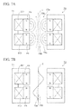
- Figs. 7A and 7B are cross-sectional views of an electron beam converging unit 70, taken along a line extending along and being parallel to the optical axis C of the electron beam converging unit 70.
- Fig. 7A shows magnetic fields with magnetic field lines
- Fig. 7B shows the strength of the magnetic fields.
- the electron beam converging unit 70 is formed of a ferromagnetic frame 71 made of pure iron or the like, and permanent magnets PA and PB and electromagnetic coils EC1 and EC2 all surrounded by the ferromagnetic frame 71.
- the permanent magnets PA and PB used are two permanent magnets each formed in a ring shape (annular shape) and magnetized in the Z-axis (optical axis C) direction. These two permanent magnets PA and PB are disposed one above the other with their same polarities facing each other. The two permanent magnets PA and PB are so disposed as to allow a gap therebetween as small as possible.
- a gap is also provided between each of the permanent magnets PA and PB and the ferromagnetic frame 71 (in a direction perpendicular to the Z-axis direction).
- the electromagnetic coils EC1 and EC2 are disposed, respectively.
- the electromagnetic coils EC1 and EC2 are wound in mutually opposite directions.
- a rare-earth magnet such for example as a neodymium magnet (Nd2Fe14B) or a samarium-cobalt magnet (SmCo5, Sm2Co17) is used.
- a rare-earth magnet is high in maximum energy product, and thus a small portion thereof can provide a large magnetic force, as compared to a ferrite magnet or an alnico magnet.
- the neodymium magnet is a sinter mainly containing iron and boron.
- the neodymium magnet is high in remanent magnetic flux density and coercivity and exerts a high magnetic energy.
- the neodymium magnet is high in mechanical strength.
- the permanent magnets PA and PB can be made small.
- a magnetic field is generated in each of the two permanent magnets PA and PB as shown in Fig. 7A .
- a magnetic field 73a is generated in a direction from the north pole of the upper permanent magnet PA to the south pole thereof above the north pole; and another magnetic field 74a is generated in a direction from the north pole of the lower permanent magnet PB to the south pole thereof below the north pole.
- broken lines 73b and 74b in Fig. 7A represent magnetic fields generated by supplying electric currents to the electromagnetic coils EC1 and EC2, respectively. As shown in Fig.
- the magnetic field 73b of the electromagnetic coil EC1 is generated at a position where it interferes with the magnetic field 73a of the permanent magnet PA
- the magnetic field 74b of the electromagnetic coil EC2 is generated at a position where it interferes with the magnetic field 74a of the permanent magnet PB.
- a solid line 75a along the optical axis C in Fig. 7B represents the strength of the magnetic fields 73a and 74a formed along the optical axis C by the respective permanent magnets PA and PB.
- the magnetic field strength is illustrated while assuming the direction of the magnetic field generated by the permanent magnet PA as a positive direction.
- the magnetic field of the permanent magnet PA reaches the maximum strength at a center portion of the permanent magnet PA in the direction of the optical axis C
- the magnetic field of the permanent magnet PB reaches the maximum strength in the negative direction at a center portion of the permanent magnet PB in the direction of the optical axis C.
- Each of the permanent magnets PA and PB is magnetized through such adjustment that it can obtain a magnetic field strength required as a lens.
- the permanent magnet after being magnetized has constant magnetic field strength, and the focal point thereof cannot be adjusted.
- the electromagnetic coil is used to make adjustment for deficiency or excess of the required magnetic field strength.
- the magnetic field strength of the permanent magnet to be increased or decreased through the adjustment by the electromagnetic coil is approximately 5%. For this reason, approximately 100 AT is large enough for the electromagnetic coil for such use. Accordingly, the electromagnetic coil does not need to be made large and can be disposed in the gap shown in Figs. 7A and 7B .
- the 7B represents the strength of the magnetic fields of the electromagnetic coils EC1 and EC2.
- the strength of the magnetic fields of the permanent magnets PA and PB can be corrected and adjusted to required magnetic field strength.
- Figs. 8A and 8B show another example of a configuration of each electron beam converging unit.
- Figs. 8A and 8B are cross-sectional views of an electron beam converging unit 80, taken along a line extending along and being parallel to the optical axis C of the electron beam converging unit 80.
- Fig. 8A shows magnetic fields with magnetic field lines
- Fig. 8B shows the strength of the magnetic fields.
- Two permanent magnets are used in the electron beam converging unit 80 shown in Figs. 8A and 8B as in the case of the electron beam converging unit 70 shown in Figs. 7A and 7B , but the arrangement of the magnets is different.
- Permanent magnets PC and PD each formed in a ring shape (annular shape) are magnetized in the Z-axis (optical axis C) direction. These two permanent magnets PC and PD are arranged in such a manner that the polarities thereof are oriented in the same direction.
- a gap is provided between the permanent magnets PC and PD.
- the permanent magnets PC and PD are surrounded by a ferromagnetic frame 81, and a gap is also provided between each of the permanent magnets PC and PD and the ferromagnetic frame 81 in the radial direction of the ferromagnetic frame 81 (in a direction perpendicular to the direction of the optical axis C).
- an electromagnetic coil EC3 is disposed.
- the permanent magnets PC and PD are provided respectively with yokes 85 on sides thereof where they face each other.
- a rare-earth magnet such as a neodymium magnet or a samarium-cobalt magnet, is used for the permanent magnets PC and PD.
- a magnetic field is generated across the two permanent magnets PC and PD as shown in Fig. 8A .
- a magnetic field 83a is generated in a direction from the north pole of the lower permanent magnet PD to the south pole of the upper permanent magnet PC.
- broken lines in Fig. 8A represent a magnetic field 83b generated by supplying an electric current to the electromagnetic coil EC3.
- the magnetic field 83b of the electromagnetic coil EC3 is generated at a position where it interferes with the magnetic field 83a of the permanent magnets PC and PD.
- Each of the permanent magnets PC and PD is magnetized through such adjustment that it can obtain a magnetic field strength required as a lens.
- the permanent magnet after being magnetized has a constant magnetic field strength, and the focal point thereof cannot be adjusted.
- the electromagnetic coil is used to make adjustment for deficiency or excess of the required magnetic field strength.
- Approximately 100 AT is large enough for the electromagnetic coil for such use. Accordingly, the electromagnetic coil does not need to be made large and can be disposed in the gap between the ferromagnetic frame 81 and the permanent magnets PC and PD, as shown in Figs. 8A and 8B .
- a broken line 84b along the optical axis C in Fig. 8B represents the strength of the magnetic field of the electromagnetic coil EC3.
- Figs. 9A and 9B show still another example of a configuration of each electron beam converging unit.
- Figs. 9A and 9B are cross-sectional views of an electron beam converging unit 90, taken along a line extending along and being parallel to the optical axis C of the electron beam converging unit 90.
- Fig. 9A shows magnetic fields with magnetic field lines
- Fig. 9B shows the strength of the magnetic fields.
- Two permanent magnets and one electromagnetic coil for correction are used in the electron beam converging unit 90 shown in Figs. 9A and 9B as in the case of the electron beam converging unit 80 shown in Figs. 8A and 8B , but the arrangement of the correction electromagnetic coil is different.
- the permanent magnets PC and PD each formed in a ring shape (annular shape) are magnetized in the Z-axis (optical axis C) direction. These two permanent magnets PC and PD are arranged in such a manner that the polarities thereof are oriented in the same direction.
- a gap is provided between the permanent magnets PC and PD. In the gap, an electromagnetic coil EC4 is disposed.
- a rare-earth magnet such as a neodymium magnet or a samarium-cobalt magnet, is used for the permanent magnets PC and PD.
- the permanent magnets PC and PD are provided respectively with yokes 95 on sides thereof where they face each other.
- a magnetic field is generated across the two permanent magnets PC and PD as shown in Fig. 9A .
- a magnetic field 93a is generated in a direction from the north pole of the lower permanent magnet PD to the south pole of the upper permanent magnet PC.
- broken lines in Fig. 9A represent a magnetic field 93b generated by supplying an electric current to the electromagnetic coil EC4.
- the magnetic field 93b of the electromagnetic coil EC4 is generated at a position where it interferes with the magnetic field 93a of the permanent magnets PC and PD.
- a solid line 94a along the optical axis C in Fig. 9B represents the strength of the magnetic field 93a formed along the optical axis C by the permanent magnets PC and PD. As shown in Fig. 9B , the magnetic field 93a reaches the maximum strength at a center portion of the gap portion between the permanent magnets PC and PD.
- a broken line 94b along the optical axis C in Fig. 9B represents the strength of the magnetic field of the electromagnetic coil EC4.
- a magnetic field of 500 G is formed on the optical axis.
- the electron beam converging unit with this configuration has magnetic field strength lower than that of the electron beam converging unit 70 configured as shown in Figs. 7A and 7B but still high enough to converge the electron beam, unless used for an objective lens.
- the electron beam converging units described above are placed in the lenses provided to the multi-column electron beam exposure apparatus. For the adjustment of each correction coil to be used there, a simulation of electron beam emission is performed to determine the electric current to be supplied to the correction coil so that the electron beam of the corresponding column would be converged on the corresponding optical axis.
- the multi-column electron beam exposure apparatus of this embodiment uses permanent magnets for the generation of magnetic fields to converge an electron beam in each column cell.
- permanent magnets having magnetic field strength high enough to converge the electron beam a neodymium magnet is used, for example.
- Use of such a permanent magnet allows reduction in the size of the magnetic field generation unit, whereby the intervals between the column cells can be reduced to 25 mm or smaller, for example.
- many column cells can be used within an area of 150 mm 2 or smaller, and the throughput can be improved.
- magnetic fields are generated by using rare-earth permanent magnets such as neodymium magnets or samarium-cobalt magnets.
- These permanent magnets are two annular permanent magnets magnetized in a direction perpendicular to the radial direction thereof and used to generate magnetic fields.
- the magnetic field strength can be made high, whereby a strong magnetic field can be generated in a small space.
- each permanent magnet is surrounded by the frame made of a ferromagnetic material such as pure iron. This makes it possible to prevent a generated magnetic field from leaking to the outside.
- an electromagnetic coil is provided near each permanent magnet, and therefore, the magnetic field strength of the permanent magnet can be adjusted by use of the magnetic field of the electromagnetic coil.
Landscapes
- Chemical & Material Sciences (AREA)
- Engineering & Computer Science (AREA)
- Nanotechnology (AREA)
- Analytical Chemistry (AREA)
- Physics & Mathematics (AREA)
- Crystallography & Structural Chemistry (AREA)
- Mathematical Physics (AREA)
- Theoretical Computer Science (AREA)
- Condensed Matter Physics & Semiconductors (AREA)
- General Physics & Mathematics (AREA)
- Manufacturing & Machinery (AREA)
- Electron Beam Exposure (AREA)
Claims (4)
- Magnetfelderzeugungsvorrichtung (90), enthaltend:zwei ringförmige Permanentmagneten (PC, PD), die in einer Richtung senkrecht zu einer radialen Richtung davon magnetisiert und übereinander angeordnet sind,eine elektromagnetische Spule (EC4), die in der Nähe der Permanentmagneten (PC, PD) angeordnet sind und verwendet werden, um ein Magnetfeld der ringförmigen Permanentmagneten (PC, PD) einzustellen, undeinen ferromagnetischen Rahmen (91), der die ringförmigen Permanentmagneten (PC, PD) und die elektromagnetische Spule (EC4) umgibt,dadurch gekennzeichnet, dass die elektromagnetische Spule (EC4) in einer Lücke zwischen den ringförmigen Permanentmagneten (PC, PD) angeordnet ist und die Polaritäten der ringförmigen Permanentmagneten (PC, PD) in derselben Richtung orientiert sind.
- Magnetfelderzeugungsvorrichtung (90) nach Anspruch 1, bei der
jeder ringförmige Permanentmagnet (PC, PD) ein Neodym-Magnet oder ein Samarium-Cobalt-Magnet ist und
der ferromagnetische Rahmen (91) aus reinem Eisen gefertigt ist. - Magnetfelderzeugungsvorrichtung nach Anspruch 1, bei der die Stärke des Magnetfelds der ringförmigen Permanentmagneten (PC, PD) innerhalb eines Bereichs von 5 % niedriger bis 5 % höher als die erforderliche Magnetfeldstärke liegt.
- Mehrsäulen-Elektronenstrahl-Belichtungsgerät, enthaltend:eine Vielzahl von Säulenzellen (11) undein Substrat (61), das mit kreisförmigen Öffnungen (63a bis 63d) versehen ist, durch welche die in den Säulenzellen (11) verwendeten Elektronenstrahlen jeweils laufen, wobei das Substrat eine Magnetfelderzeugungsvorrichtung (90) nach einem der Ansprüche 1 bis 3 aufweist, die in einem Seitenbereich (64a bis 64d) einer jeden kreisförmigen Öffnung (63a bis 63d) angeordnet ist.
Applications Claiming Priority (1)
| Application Number | Priority Date | Filing Date | Title |
|---|---|---|---|
| PCT/JP2008/061431 WO2009157054A1 (ja) | 2008-06-24 | 2008-06-24 | マルチコラム電子ビーム露光装置及び磁場発生装置 |
Publications (3)
| Publication Number | Publication Date |
|---|---|
| EP2302664A1 EP2302664A1 (de) | 2011-03-30 |
| EP2302664A4 EP2302664A4 (de) | 2011-09-28 |
| EP2302664B1 true EP2302664B1 (de) | 2013-11-06 |
Family
ID=41444132
Family Applications (1)
| Application Number | Title | Priority Date | Filing Date |
|---|---|---|---|
| EP08790570.9A Active EP2302664B1 (de) | 2008-06-24 | 2008-06-24 | MEHRSÄULEN-ELEKTRONENSTRAHLBELICHTUNGSVORRICHTUNG UND Vorrichtung zur Erzeugung eines Magnetfeldes |
Country Status (4)
| Country | Link |
|---|---|
| US (1) | US8390201B2 (de) |
| EP (1) | EP2302664B1 (de) |
| JP (1) | JP5363480B2 (de) |
| WO (1) | WO2009157054A1 (de) |
Families Citing this family (19)
| Publication number | Priority date | Publication date | Assignee | Title |
|---|---|---|---|---|
| GB201005412D0 (en) * | 2010-03-31 | 2010-05-19 | E2V Tech Uk Ltd | Magnetron |
| CN103038855B (zh) | 2010-10-27 | 2016-02-03 | 株式会社Param | 电子透镜和电子束装置 |
| US8445862B2 (en) * | 2010-12-14 | 2013-05-21 | Hermes Microvision, Inc. | Apparatus of plural charged particle beams with multi-axis magnetic lens |
| US8455838B2 (en) | 2011-06-29 | 2013-06-04 | Kla-Tencor Corporation | Multiple-column electron beam apparatus and methods |
| US9000394B2 (en) * | 2011-12-20 | 2015-04-07 | Hermes Microvision, Inc. | Multi-axis magnetic lens for focusing a plurality of charged particle beams |
| US8835867B2 (en) * | 2012-01-17 | 2014-09-16 | Hermes-Microvision, Inc. | Multi-axis magnetic lens for focusing a plurality of charged particle beams |
| US8710428B1 (en) * | 2012-02-22 | 2014-04-29 | AOSense, Inc. | Permanent magnet axial field zeeman slower |
| US10047912B2 (en) | 2013-10-15 | 2018-08-14 | LIFI Labs, Inc. | Lighting assembly |
| US11455884B2 (en) | 2014-09-02 | 2022-09-27 | LIFI Labs, Inc. | Lighting system |
| CN105900531B (zh) | 2013-11-14 | 2019-03-29 | 莱弗实验室公司 | 可复位的照明系统及方法 |
| EP3146254B1 (de) | 2014-05-22 | 2020-04-22 | Lifi Labs Inc. | Direktionales beleuchtungssystem und verfahren |
| US9711314B2 (en) * | 2014-09-11 | 2017-07-18 | Larry R. Barnett | Compact magnet system for a high-power millimeter-wave gyrotron |
| GB2534404A (en) * | 2015-01-23 | 2016-07-27 | Cnm Tech Gmbh | Pellicle |
| JP6470124B2 (ja) * | 2015-06-19 | 2019-02-13 | 株式会社東芝 | 粒子線ビームの制御電磁石及びこれを備えた照射治療装置 |
| JP2017204499A (ja) | 2016-05-09 | 2017-11-16 | 株式会社アドバンテスト | マルチカラム荷電粒子ビーム露光装置 |
| US10440794B2 (en) | 2016-11-02 | 2019-10-08 | LIFI Labs, Inc. | Lighting system and method |
| WO2018189817A1 (ja) * | 2017-04-11 | 2018-10-18 | 株式会社アドバンテスト | 露光装置 |
| WO2018198222A1 (ja) * | 2017-04-26 | 2018-11-01 | 株式会社ニコン | 露光装置、露光方法、及び、デバイス製造方法 |
| EP3881347A1 (de) * | 2018-11-16 | 2021-09-22 | ASML Netherlands B.V. | Elektromagnetische zusammengesetzte linse und optisches system mit geladenen teilchen mit einer solchen linse |
Family Cites Families (19)
| Publication number | Priority date | Publication date | Assignee | Title |
|---|---|---|---|---|
| US2503173A (en) * | 1946-10-18 | 1950-04-04 | Rca Corp | Permanent magnetic electron lens system |
| JPS51122373A (en) * | 1975-04-18 | 1976-10-26 | Hitachi Ltd | Electric microscope |
| JPS52100195A (en) * | 1976-02-18 | 1977-08-22 | Hitachi Ltd | Permanent magnet for electronic lens |
| JPS55143761A (en) * | 1979-04-24 | 1980-11-10 | Hitachi Metals Ltd | Focus magnet |
| JPS5914242A (ja) * | 1982-07-15 | 1984-01-25 | Hitachi Ltd | 電磁レンズ |
| CN86105432A (zh) * | 1985-09-27 | 1987-05-27 | 美国电话电报公司 | 带电粒子束曝光 |
| GB2192092A (en) * | 1986-06-25 | 1987-12-31 | Philips Electronic Associated | Magnetic lens system |
| JPH0654643B2 (ja) * | 1987-09-14 | 1994-07-20 | 日本電子株式会社 | 電界放射型電子銃用レンズ |
| JPH01166450A (ja) * | 1987-12-23 | 1989-06-30 | Hitachi Ltd | 荷電粒子光学系 |
| JPH05128986A (ja) * | 1991-11-06 | 1993-05-25 | Jeol Ltd | 磁場型レンズ |
| WO1999053600A1 (en) * | 1998-04-10 | 1999-10-21 | Nikon Corporation | Linear motor having polygonal coil unit |
| JP3799874B2 (ja) * | 1999-06-15 | 2006-07-19 | Kddi株式会社 | 偏波モード分散補償装置 |
| US20020036367A1 (en) * | 2000-02-22 | 2002-03-28 | Marlin Walmer | Method for producing & manufacturing density enhanced, DMC, bonded permanent magnets |
| JP4301724B2 (ja) * | 2000-12-06 | 2009-07-22 | 株式会社アドバンテスト | 電子ビーム露光装置及び電子レンズ |
| JP4156862B2 (ja) * | 2002-05-10 | 2008-09-24 | 株式会社アドバンテスト | 電子ビーム露光装置及び電子ビーム処理装置 |
| JP4327497B2 (ja) | 2002-06-26 | 2009-09-09 | 株式会社アドバンテスト | 電子ビーム露光装置、電子ビーム露光方法、半導体素子製造方法、マスク、及びマスク製造方法 |
| NL1023260C1 (nl) * | 2003-04-24 | 2004-10-27 | Fei Co | Deeltjes-optisch apparaat met een permanent magnetische lens en een elektrostatische lens. |
| GB2408143B (en) * | 2003-10-20 | 2006-11-15 | Ims Nanofabrication Gmbh | Charged-particle multi-beam exposure apparatus |
| WO2006018840A2 (en) * | 2004-08-16 | 2006-02-23 | Ellumina Vision Ltd. | Electron microscope array for inspection and lithography |
-
2008
- 2008-06-24 EP EP08790570.9A patent/EP2302664B1/de active Active
- 2008-06-24 JP JP2010517612A patent/JP5363480B2/ja active Active
- 2008-06-24 WO PCT/JP2008/061431 patent/WO2009157054A1/ja not_active Ceased
-
2010
- 2010-12-22 US US12/928,899 patent/US8390201B2/en active Active
Also Published As
| Publication number | Publication date |
|---|---|
| JPWO2009157054A1 (ja) | 2011-12-01 |
| EP2302664A4 (de) | 2011-09-28 |
| US20110148297A1 (en) | 2011-06-23 |
| EP2302664A1 (de) | 2011-03-30 |
| US8390201B2 (en) | 2013-03-05 |
| WO2009157054A1 (ja) | 2009-12-30 |
| JP5363480B2 (ja) | 2013-12-11 |
Similar Documents
| Publication | Publication Date | Title |
|---|---|---|
| EP2302664B1 (de) | MEHRSÄULEN-ELEKTRONENSTRAHLBELICHTUNGSVORRICHTUNG UND Vorrichtung zur Erzeugung eines Magnetfeldes | |
| KR100926398B1 (ko) | 리본 모양의 주입기 이온 빔의 특성 제어 | |
| US8058626B2 (en) | Method and apparatus for modifying a ribbon-shaped ion beam | |
| EP4120314B1 (de) | Elektromagnetische linse | |
| JP5149203B2 (ja) | 電磁石、イオン注入システム、イオン注入システム用のフィルタリングシステム、質量分析に用いる電磁石、および開口フレーム型電磁石の磁場を閉じ込める方法 | |
| JP2003332207A (ja) | 電子ビーム露光装置及び電子ビーム処理装置 | |
| US6005250A (en) | Illumination deflection system for E-beam projection | |
| US20030111614A1 (en) | Stage devices including linear motors that produce reduced beam-perturbing stray magnetic fields, and charged-particle-beam microlithography systems comprising same | |
| US20240242933A1 (en) | Multi charged particle beam writing apparatus | |
| US20240242920A1 (en) | Multi charged particle beam writing apparatus | |
| US6710361B2 (en) | Multi-beam hybrid solenoid lens electron beam system | |
| US20240242919A1 (en) | Multi charged particle beam writing apparatus | |
| US20240212970A1 (en) | Adjustable Magnetic Lens Having Permanent-Magnetic and Electromagnetic Components | |
| JP2016219292A (ja) | 電子レンズおよびマルチコラム電子ビーム装置 | |
| JP2009065193A (ja) | 電子ビーム描画方法及びその装置 | |
| US12580148B2 (en) | Multi charged particle beam writing apparatus | |
| US6489620B1 (en) | Astigmatism-correction device and charged-particle-beam microlithography apparatus and methods comprising same | |
| JP2019212680A (ja) | マルチ荷電粒子ビーム描画装置及びその調整方法 | |
| WO2025225123A1 (ja) | マルチ荷電粒子ビーム照射装置 | |
| WO2009113169A1 (ja) | マルチコラム電子ビーム露光装置 | |
| JP2010129421A (ja) | 電子レンズ用磁気回路装置 |
Legal Events
| Date | Code | Title | Description |
|---|---|---|---|
| PUAI | Public reference made under article 153(3) epc to a published international application that has entered the european phase |
Free format text: ORIGINAL CODE: 0009012 |
|
| 17P | Request for examination filed |
Effective date: 20101223 |
|
| AK | Designated contracting states |
Kind code of ref document: A1 Designated state(s): AT BE BG CH CY CZ DE DK EE ES FI FR GB GR HR HU IE IS IT LI LT LU LV MC MT NL NO PL PT RO SE SI SK TR |
|
| AX | Request for extension of the european patent |
Extension state: AL BA MK RS |
|
| A4 | Supplementary search report drawn up and despatched |
Effective date: 20110826 |
|
| DAX | Request for extension of the european patent (deleted) | ||
| RIC1 | Information provided on ipc code assigned before grant |
Ipc: H01J 37/14 20060101ALI20110822BHEP Ipc: H01J 37/143 20060101AFI20110822BHEP Ipc: H01J 37/317 20060101ALI20110822BHEP |
|
| REG | Reference to a national code |
Ref country code: DE Ref legal event code: R079 Ref document number: 602008028598 Country of ref document: DE Free format text: PREVIOUS MAIN CLASS: H01L0021027000 Ipc: H01J0037317000 |
|
| GRAP | Despatch of communication of intention to grant a patent |
Free format text: ORIGINAL CODE: EPIDOSNIGR1 |
|
| RIC1 | Information provided on ipc code assigned before grant |
Ipc: H01J 37/06 20060101ALI20130710BHEP Ipc: H01J 37/317 20060101AFI20130710BHEP Ipc: B82Y 10/00 20110101ALI20130710BHEP Ipc: B82Y 40/00 20110101ALI20130710BHEP Ipc: H01J 37/14 20060101ALI20130710BHEP Ipc: H01J 37/143 20060101ALI20130710BHEP |
|
| INTG | Intention to grant announced |
Effective date: 20130806 |
|
| GRAS | Grant fee paid |
Free format text: ORIGINAL CODE: EPIDOSNIGR3 |
|
| GRAA | (expected) grant |
Free format text: ORIGINAL CODE: 0009210 |
|
| AK | Designated contracting states |
Kind code of ref document: B1 Designated state(s): AT BE BG CH CY CZ DE DK EE ES FI FR GB GR HR HU IE IS IT LI LT LU LV MC MT NL NO PL PT RO SE SI SK TR |
|
| REG | Reference to a national code |
Ref country code: GB Ref legal event code: FG4D |
|
| REG | Reference to a national code |
Ref country code: CH Ref legal event code: EP |
|
| REG | Reference to a national code |
Ref country code: AT Ref legal event code: REF Ref document number: 639947 Country of ref document: AT Kind code of ref document: T Effective date: 20131215 |
|
| REG | Reference to a national code |
Ref country code: IE Ref legal event code: FG4D |
|
| REG | Reference to a national code |
Ref country code: DE Ref legal event code: R096 Ref document number: 602008028598 Country of ref document: DE Effective date: 20131224 |
|
| REG | Reference to a national code |
Ref country code: NL Ref legal event code: VDEP Effective date: 20131106 |
|
| REG | Reference to a national code |
Ref country code: AT Ref legal event code: MK05 Ref document number: 639947 Country of ref document: AT Kind code of ref document: T Effective date: 20131106 |
|
| REG | Reference to a national code |
Ref country code: LT Ref legal event code: MG4D |
|
| PG25 | Lapsed in a contracting state [announced via postgrant information from national office to epo] |
Ref country code: FI Free format text: LAPSE BECAUSE OF FAILURE TO SUBMIT A TRANSLATION OF THE DESCRIPTION OR TO PAY THE FEE WITHIN THE PRESCRIBED TIME-LIMIT Effective date: 20131106 Ref country code: IS Free format text: LAPSE BECAUSE OF FAILURE TO SUBMIT A TRANSLATION OF THE DESCRIPTION OR TO PAY THE FEE WITHIN THE PRESCRIBED TIME-LIMIT Effective date: 20140306 Ref country code: NL Free format text: LAPSE BECAUSE OF FAILURE TO SUBMIT A TRANSLATION OF THE DESCRIPTION OR TO PAY THE FEE WITHIN THE PRESCRIBED TIME-LIMIT Effective date: 20131106 Ref country code: NO Free format text: LAPSE BECAUSE OF FAILURE TO SUBMIT A TRANSLATION OF THE DESCRIPTION OR TO PAY THE FEE WITHIN THE PRESCRIBED TIME-LIMIT Effective date: 20140206 Ref country code: HR Free format text: LAPSE BECAUSE OF FAILURE TO SUBMIT A TRANSLATION OF THE DESCRIPTION OR TO PAY THE FEE WITHIN THE PRESCRIBED TIME-LIMIT Effective date: 20131106 Ref country code: LT Free format text: LAPSE BECAUSE OF FAILURE TO SUBMIT A TRANSLATION OF THE DESCRIPTION OR TO PAY THE FEE WITHIN THE PRESCRIBED TIME-LIMIT Effective date: 20131106 Ref country code: SE Free format text: LAPSE BECAUSE OF FAILURE TO SUBMIT A TRANSLATION OF THE DESCRIPTION OR TO PAY THE FEE WITHIN THE PRESCRIBED TIME-LIMIT Effective date: 20131106 |
|
| PG25 | Lapsed in a contracting state [announced via postgrant information from national office to epo] |
Ref country code: BE Free format text: LAPSE BECAUSE OF FAILURE TO SUBMIT A TRANSLATION OF THE DESCRIPTION OR TO PAY THE FEE WITHIN THE PRESCRIBED TIME-LIMIT Effective date: 20131106 Ref country code: AT Free format text: LAPSE BECAUSE OF FAILURE TO SUBMIT A TRANSLATION OF THE DESCRIPTION OR TO PAY THE FEE WITHIN THE PRESCRIBED TIME-LIMIT Effective date: 20131106 Ref country code: ES Free format text: LAPSE BECAUSE OF FAILURE TO SUBMIT A TRANSLATION OF THE DESCRIPTION OR TO PAY THE FEE WITHIN THE PRESCRIBED TIME-LIMIT Effective date: 20131106 Ref country code: LV Free format text: LAPSE BECAUSE OF FAILURE TO SUBMIT A TRANSLATION OF THE DESCRIPTION OR TO PAY THE FEE WITHIN THE PRESCRIBED TIME-LIMIT Effective date: 20131106 |
|
| PG25 | Lapsed in a contracting state [announced via postgrant information from national office to epo] |
Ref country code: PT Free format text: LAPSE BECAUSE OF FAILURE TO SUBMIT A TRANSLATION OF THE DESCRIPTION OR TO PAY THE FEE WITHIN THE PRESCRIBED TIME-LIMIT Effective date: 20140306 |
|
| PG25 | Lapsed in a contracting state [announced via postgrant information from national office to epo] |
Ref country code: EE Free format text: LAPSE BECAUSE OF FAILURE TO SUBMIT A TRANSLATION OF THE DESCRIPTION OR TO PAY THE FEE WITHIN THE PRESCRIBED TIME-LIMIT Effective date: 20131106 |
|
| REG | Reference to a national code |
Ref country code: DE Ref legal event code: R097 Ref document number: 602008028598 Country of ref document: DE |
|
| PG25 | Lapsed in a contracting state [announced via postgrant information from national office to epo] |
Ref country code: CZ Free format text: LAPSE BECAUSE OF FAILURE TO SUBMIT A TRANSLATION OF THE DESCRIPTION OR TO PAY THE FEE WITHIN THE PRESCRIBED TIME-LIMIT Effective date: 20131106 Ref country code: IT Free format text: LAPSE BECAUSE OF FAILURE TO SUBMIT A TRANSLATION OF THE DESCRIPTION OR TO PAY THE FEE WITHIN THE PRESCRIBED TIME-LIMIT Effective date: 20131106 Ref country code: RO Free format text: LAPSE BECAUSE OF FAILURE TO SUBMIT A TRANSLATION OF THE DESCRIPTION OR TO PAY THE FEE WITHIN THE PRESCRIBED TIME-LIMIT Effective date: 20131106 Ref country code: SK Free format text: LAPSE BECAUSE OF FAILURE TO SUBMIT A TRANSLATION OF THE DESCRIPTION OR TO PAY THE FEE WITHIN THE PRESCRIBED TIME-LIMIT Effective date: 20131106 Ref country code: PL Free format text: LAPSE BECAUSE OF FAILURE TO SUBMIT A TRANSLATION OF THE DESCRIPTION OR TO PAY THE FEE WITHIN THE PRESCRIBED TIME-LIMIT Effective date: 20131106 |
|
| PLBE | No opposition filed within time limit |
Free format text: ORIGINAL CODE: 0009261 |
|
| STAA | Information on the status of an ep patent application or granted ep patent |
Free format text: STATUS: NO OPPOSITION FILED WITHIN TIME LIMIT |
|
| PG25 | Lapsed in a contracting state [announced via postgrant information from national office to epo] |
Ref country code: DK Free format text: LAPSE BECAUSE OF FAILURE TO SUBMIT A TRANSLATION OF THE DESCRIPTION OR TO PAY THE FEE WITHIN THE PRESCRIBED TIME-LIMIT Effective date: 20131106 |
|
| 26N | No opposition filed |
Effective date: 20140807 |
|
| REG | Reference to a national code |
Ref country code: DE Ref legal event code: R097 Ref document number: 602008028598 Country of ref document: DE Effective date: 20140807 |
|
| PG25 | Lapsed in a contracting state [announced via postgrant information from national office to epo] |
Ref country code: LU Free format text: LAPSE BECAUSE OF FAILURE TO SUBMIT A TRANSLATION OF THE DESCRIPTION OR TO PAY THE FEE WITHIN THE PRESCRIBED TIME-LIMIT Effective date: 20140624 Ref country code: MC Free format text: LAPSE BECAUSE OF FAILURE TO SUBMIT A TRANSLATION OF THE DESCRIPTION OR TO PAY THE FEE WITHIN THE PRESCRIBED TIME-LIMIT Effective date: 20131106 |
|
| REG | Reference to a national code |
Ref country code: CH Ref legal event code: PL |
|
| GBPC | Gb: european patent ceased through non-payment of renewal fee |
Effective date: 20140624 |
|
| PG25 | Lapsed in a contracting state [announced via postgrant information from national office to epo] |
Ref country code: SI Free format text: LAPSE BECAUSE OF FAILURE TO SUBMIT A TRANSLATION OF THE DESCRIPTION OR TO PAY THE FEE WITHIN THE PRESCRIBED TIME-LIMIT Effective date: 20131106 |
|
| REG | Reference to a national code |
Ref country code: IE Ref legal event code: MM4A |
|
| REG | Reference to a national code |
Ref country code: FR Ref legal event code: ST Effective date: 20150227 |
|
| PG25 | Lapsed in a contracting state [announced via postgrant information from national office to epo] |
Ref country code: IE Free format text: LAPSE BECAUSE OF NON-PAYMENT OF DUE FEES Effective date: 20140624 Ref country code: LI Free format text: LAPSE BECAUSE OF NON-PAYMENT OF DUE FEES Effective date: 20140630 Ref country code: CH Free format text: LAPSE BECAUSE OF NON-PAYMENT OF DUE FEES Effective date: 20140630 |
|
| PG25 | Lapsed in a contracting state [announced via postgrant information from national office to epo] |
Ref country code: FR Free format text: LAPSE BECAUSE OF NON-PAYMENT OF DUE FEES Effective date: 20140630 Ref country code: GB Free format text: LAPSE BECAUSE OF NON-PAYMENT OF DUE FEES Effective date: 20140624 |
|
| PG25 | Lapsed in a contracting state [announced via postgrant information from national office to epo] |
Ref country code: MT Free format text: LAPSE BECAUSE OF FAILURE TO SUBMIT A TRANSLATION OF THE DESCRIPTION OR TO PAY THE FEE WITHIN THE PRESCRIBED TIME-LIMIT Effective date: 20131106 |
|
| PG25 | Lapsed in a contracting state [announced via postgrant information from national office to epo] |
Ref country code: BG Free format text: LAPSE BECAUSE OF FAILURE TO SUBMIT A TRANSLATION OF THE DESCRIPTION OR TO PAY THE FEE WITHIN THE PRESCRIBED TIME-LIMIT Effective date: 20131106 |
|
| PG25 | Lapsed in a contracting state [announced via postgrant information from national office to epo] |
Ref country code: CY Free format text: LAPSE BECAUSE OF FAILURE TO SUBMIT A TRANSLATION OF THE DESCRIPTION OR TO PAY THE FEE WITHIN THE PRESCRIBED TIME-LIMIT Effective date: 20131106 Ref country code: GR Free format text: LAPSE BECAUSE OF FAILURE TO SUBMIT A TRANSLATION OF THE DESCRIPTION OR TO PAY THE FEE WITHIN THE PRESCRIBED TIME-LIMIT Effective date: 20140207 |
|
| PG25 | Lapsed in a contracting state [announced via postgrant information from national office to epo] |
Ref country code: HU Free format text: LAPSE BECAUSE OF FAILURE TO SUBMIT A TRANSLATION OF THE DESCRIPTION OR TO PAY THE FEE WITHIN THE PRESCRIBED TIME-LIMIT; INVALID AB INITIO Effective date: 20080624 Ref country code: TR Free format text: LAPSE BECAUSE OF FAILURE TO SUBMIT A TRANSLATION OF THE DESCRIPTION OR TO PAY THE FEE WITHIN THE PRESCRIBED TIME-LIMIT Effective date: 20131106 |
|
| P01 | Opt-out of the competence of the unified patent court (upc) registered |
Effective date: 20230529 |
|
| PGFP | Annual fee paid to national office [announced via postgrant information from national office to epo] |
Ref country code: DE Payment date: 20250507 Year of fee payment: 18 |