EP2302781A2 - Procédé de génération d'une tension de sortie avec une valeur efficace d'une liaison intermédiaire en continu - Google Patents
Procédé de génération d'une tension de sortie avec une valeur efficace d'une liaison intermédiaire en continu Download PDFInfo
- Publication number
- EP2302781A2 EP2302781A2 EP10180515A EP10180515A EP2302781A2 EP 2302781 A2 EP2302781 A2 EP 2302781A2 EP 10180515 A EP10180515 A EP 10180515A EP 10180515 A EP10180515 A EP 10180515A EP 2302781 A2 EP2302781 A2 EP 2302781A2
- Authority
- EP
- European Patent Office
- Prior art keywords
- counter
- value
- output voltage
- voltage
- generating
- Prior art date
- Legal status (The legal status is an assumption and is not a legal conclusion. Google has not performed a legal analysis and makes no representation as to the accuracy of the status listed.)
- Granted
Links
Images

Classifications
-
- H—ELECTRICITY
- H02—GENERATION; CONVERSION OR DISTRIBUTION OF ELECTRIC POWER
- H02M—APPARATUS FOR CONVERSION BETWEEN AC AND AC, BETWEEN AC AND DC, OR BETWEEN DC AND DC, AND FOR USE WITH MAINS OR SIMILAR POWER SUPPLY SYSTEMS; CONVERSION OF DC OR AC INPUT POWER INTO SURGE OUTPUT POWER; CONTROL OR REGULATION THEREOF
- H02M7/00—Conversion of AC power input into DC power output; Conversion of DC power input into AC power output
- H02M7/42—Conversion of DC power input into AC power output without possibility of reversal
- H02M7/44—Conversion of DC power input into AC power output without possibility of reversal by static converters
- H02M7/48—Conversion of DC power input into AC power output without possibility of reversal by static converters using discharge tubes with control electrode or semiconductor devices with control electrode
Definitions
- the invention relates to a method for generating an output voltage with an adjustable effective value from a variable DC link voltage.
- Umrichter In electric drive systems with electric motors usually so-called (frequency) Umrichter be used to generate an AC voltage an output voltage with adjustable frequency and amplitude, which serves to control the electric motors.
- a converter for this purpose first the AC line voltage is rectified in a so-called DC link voltage, which is usually transformed by means of so-called switching bridges in the output voltage with adjustable frequency.
- the intermediate circuit voltage is usually subjected to pulse width modulation, whereby the effective value depends on the selected pulse width modulation duty cycle.
- the resulting effective value of the output voltage depends not only on the set duty cycle but also on a current value the DC link voltage from.
- the DC link voltage in turn depends on many factors, for example on the instantaneous mains voltage, on a current load of the converter and / or on other converters operating in a so-called converter network.
- a counter is usually used in conjunction with a comparator or comparator, wherein the counter is operated or incremented with a counter clock signal with a constant counter clock frequency.
- the desired duty cycle is set by calculating appropriate counter setpoints.
- the counter setpoints are compared with the current counter value, whereby a level of the output voltage is set in dependence on a result of the comparison.
- the counter setpoints are calculated as a function of the instantaneous intermediate circuit voltage, which requires a division.
- divisions in smaller microprocessors commonly used in converters require a significant amount of computation time, causing undesirable dead times in regulating the output voltage. Such dead times, for example, require higher capacitance values for the DC link capacitors used and generally impair the quality of control.
- the invention has for its object to provide a method for generating an output voltage with an adjustable effective value from a variable DC link voltage available, which allows consideration of a current value of the DC link voltage in the generation of the output voltage with the least possible computational load.
- the invention solves this problem by a method having the features of claim 1.
- the rms value of the output voltage is set by means of a pulse width modulation of the intermediate circuit voltage.
- the instantaneous intermediate circuit voltage is measured.
- a counter clock signal is then generated with a counter clock frequency which is proportional to the measured intermediate circuit voltage.
- At least one counter setpoint is generated, which depends on a set rms value of the output voltage.
- Counter values are generated in time with the counter clock signal, for example, a counter is incremented in time with the counter clock signal, the output voltage being generated as a pulse width modulated signal by comparing the instantaneous counter value with the at least one counter setpoint, wherein a level of the output voltage is dependent on the result of the counter Comparative is set.
- counter values are generated in the inventive method based on a counter clock signal with variable counter clock frequency, wherein the counter clock frequency is proportional to the instantaneous DC link voltage, which can be dispensed with a division.
- the counter clock frequency increases according to the invention in proportion to the measured intermediate circuit voltage.
- a first counter setpoint value and a second counter setpoint value are generated, wherein a difference between the first counter setpoint value and the second counter setpoint value depends exclusively on the adjusted rms value of the output voltage.
- the difference between the first counter setpoint and the second counter setpoint value does not depend on the intermediate circuit voltage.
- a level of the output voltage is set to a first value, such as the intermediate circuit voltage, when the counter value is greater than or equal to the first counter setpoint and less than or equal to the second counter setpoint, and otherwise the level of the output voltage becomes a second value, for example OV, set.
- the counter value is reset to an initial value, for example zero, when a predetermined, in particular constant, period duration of the pulse-width-modulated signal or the output voltage has expired.
- the specified period may be in the range of 0.01 ms to 100 ms, for example. It is preferably 1 ms.
- Fig. 1 shows a block diagram of a device for generating an output voltage US with an adjustable effective value of a variable intermediate circuit voltage UZK.
- the device shown is part of a non-illustrated, conventional (frequency) converter, which is used to control not shown electric motors of an electric drive system.
- the device comprises a frequency divider unit 10, which is supplied with a system clock signal having a frequency f1, a digital value UZK_D, which corresponds to the instantaneous or actual intermediate circuit voltage UZK, and a digital normalization value UZK_N.
- the meter clock frequency fc is therefore proportional to the measured intermediate circuit voltage UZK or its digital equivalent UZK_D.
- the frequency divider unit 10 includes a summer 11, a clock clocked by the system clock signal or flip-flop 12, a multiplexer 13, a subtracter 14 and a comparator 15, which are interconnected in the manner shown.
- a frequency divider unit is for example in the US 4,816,774 to which reference is made in order to avoid a redundant functional description.
- the counter clock signal with the frequency fc is used to supply a counter / comparator 20 with a clock signal.
- the counter / comparator 20 is further supplied with a counter setpoint ZS and increments counter values in the clock cycle fc of the counter clock signal.
- the counter / comparator 20 generates an intermediate output voltage US 'as a pulse width modulated signal by comparing the current counter value with the counter setpoint value ZS, setting a level of the intermediate output voltage US' depending on the result of the comparison.
- the counter / comparator 20 generates the intermediate output voltage US 'at a logic level of 1 when the counter value is smaller than the counter setpoint ZS, otherwise the intermediate output voltage US' is generated at a logic level of zero.
- the intermediate output voltage US ' is converted by means of a driver unit 40 in terms of their level to the intermediate circuit voltage UZK.
- the intermediate circuit voltage UZK is output at the output of the driver unit and at a logic level 0 of the intermediate output voltage US' 40 ground voltage is output at the output of the driver unit.
- a timer unit 30 resets the counter value of counter / comparator 20 to an initial value of zero when a predetermined period of time, for example 1 ms, has elapsed.
- the timer unit 30 thus determines the period of the pulse width modulated output signal US 'or US.
- the digital normalization value UZK_N is 1000
- the instantaneous intermediate circuit voltage is UZK_D 100 in digital representation
- a set effective value of the output voltage is US 50V
- the frequency f1 of the system clock signal is constant 100 kHz
- a period TP of the pulse width modulated output voltage US is constant 1 ms.
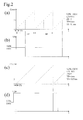
- the duty cycle i. the ratio of the length of the switched-on state (pulse duration) to the period TP, 0.5 or 50%. This corresponds to a counter setpoint ZS of 5.
- the intermediate circuit voltage UZK to a value of 200V or the digital representation UZK_D to 200
- the counter setpoint remains constant, i. is independent of the actual intermediate circuit voltage UZK, the counter value 5 is already halfway through the time, i. 0.25ms. Since the period TP is constant 1 ms, an output voltage with a duty cycle of 25% is generated in this way, which corresponds to an effective value of 50V at the current DC link voltage of 200V.
- the duty cycle is at a constant period TP Inversely proportional to the current DC link voltage UZK, whereby a consideration, ie compensation, the current DC link voltage UZK in the generation of the rms value of the output voltage US is possible, without requiring the counter setpoint ZS is to recalculate using a division. This considerably reduces the necessary computing power, as a result of which dead time-related dead times can be avoided and the quality of the control increases.
- the pulses of the pulse width modulated output voltage US are left justified in the cycle, i. a pulse starts at the beginning of each cycle. Depending on the application, however, it may be better to center the pulses within one cycle.
- two counter setpoint values ZS1 and ZS2 are to be calculated, wherein, for example, the first counter setpoint value ZS1 defines a switch-on time and the second counter setpoint value ZS2 defines a switch-off time point of a pulse-width-modulated output voltage US pulse.
- the value TP_D denotes the period TP in counter increments and US_D the effective value of the output voltage in digital representation.
- a difference between the first counter setpoint ZS1 and the second counter setpoint ZS2 depends exclusively on the set effective value of the output voltage US_D. Also in this calculation of the counter setpoint values ZS1 and ZS2 can be dispensed with a floating-point division, since the division by two by means of a shift operation can be realized.
- the counter / comparator 20 is operated with a variable clock which is proportional to the intermediate circuit voltage UZK, which corresponds to the result of the conventional division in the calculation of the counter setpoints.
- the clock setting takes place here by means of the frequency divider unit 10, i. a computation-intensive division operation in the calculation of the counter or the setpoint values can be omitted.
Landscapes
- Engineering & Computer Science (AREA)
- Power Engineering (AREA)
- Dc-Dc Converters (AREA)
- Inverter Devices (AREA)
Applications Claiming Priority (1)
| Application Number | Priority Date | Filing Date | Title |
|---|---|---|---|
| DE200910048550 DE102009048550A1 (de) | 2009-09-29 | 2009-09-29 | Verfahren zum Erzeugen einer Ausgangsspannung |
Publications (3)
| Publication Number | Publication Date |
|---|---|
| EP2302781A2 true EP2302781A2 (fr) | 2011-03-30 |
| EP2302781A3 EP2302781A3 (fr) | 2012-09-26 |
| EP2302781B1 EP2302781B1 (fr) | 2018-07-18 |
Family
ID=43447164
Family Applications (1)
| Application Number | Title | Priority Date | Filing Date |
|---|---|---|---|
| EP10180515.8A Not-in-force EP2302781B1 (fr) | 2009-09-29 | 2010-09-28 | Procédé de génération d'une tension de sortie avec une valeur efficace d'une liaison intermédiaire en continu |
Country Status (2)
| Country | Link |
|---|---|
| EP (1) | EP2302781B1 (fr) |
| DE (1) | DE102009048550A1 (fr) |
Cited By (1)
| Publication number | Priority date | Publication date | Assignee | Title |
|---|---|---|---|---|
| EP3109651A1 (fr) | 2015-06-25 | 2016-12-28 | Lenze Automation Gmbh | Procédé pour la détermination d'au moins une grandeur caractéristique d'une machine électrique et convertisseur de fréquence |
Citations (1)
| Publication number | Priority date | Publication date | Assignee | Title |
|---|---|---|---|---|
| US4816774A (en) | 1988-06-03 | 1989-03-28 | Motorola, Inc. | Frequency synthesizer with spur compensation |
Family Cites Families (7)
| Publication number | Priority date | Publication date | Assignee | Title |
|---|---|---|---|---|
| AT400273B (de) * | 1986-05-27 | 1995-11-27 | Austria Antriebstech | Drehstromantrieb mit frequenzumrichtersteuerung |
| EP0387686A3 (fr) * | 1989-03-17 | 1993-03-17 | Siemens Aktiengesellschaft | Procédé de conversion de tension en fréquence et dispositif de réalisation dudit procédé |
| WO1993004526A1 (fr) * | 1991-08-22 | 1993-03-04 | Siemens Aktiengesellschaft | Procede et dispositif de reglage en fonction d'une grandeur de reglage prescrite continue des valeurs moyennes d'une grandeur de reglage derivee d'une grandeur d'entree commutee |
| DE69533001T2 (de) * | 1995-10-06 | 2005-05-04 | Hitachi, Ltd. | Motorregler |
| US7376182B2 (en) * | 2004-08-23 | 2008-05-20 | Microchip Technology Incorporated | Digital processor with pulse width modulation module having dynamically adjustable phase offset capability, high speed operation and simultaneous update of multiple pulse width modulation duty cycle registers |
| DE102005012658A1 (de) * | 2005-03-18 | 2006-09-28 | Siemens Ag | Verfahren zur Korrektur einer Stellgröße eines selbstgeführten Pulsstromrichters eines Spannungszwischenkreis-Umrichters mit Netzgrundschwingung getakteter Einspeisung |
| AT505734A1 (de) * | 2007-09-11 | 2009-03-15 | Siemens Ag Oesterreich | Verfahren zur regelung eines schaltwandlers |
-
2009
- 2009-09-29 DE DE200910048550 patent/DE102009048550A1/de not_active Withdrawn
-
2010
- 2010-09-28 EP EP10180515.8A patent/EP2302781B1/fr not_active Not-in-force
Patent Citations (1)
| Publication number | Priority date | Publication date | Assignee | Title |
|---|---|---|---|---|
| US4816774A (en) | 1988-06-03 | 1989-03-28 | Motorola, Inc. | Frequency synthesizer with spur compensation |
Cited By (3)
| Publication number | Priority date | Publication date | Assignee | Title |
|---|---|---|---|---|
| EP3109651A1 (fr) | 2015-06-25 | 2016-12-28 | Lenze Automation Gmbh | Procédé pour la détermination d'au moins une grandeur caractéristique d'une machine électrique et convertisseur de fréquence |
| DE102015211860A1 (de) | 2015-06-25 | 2016-12-29 | Lenze Automation Gmbh | Verfahren zum Ermitteln mindestens einer Kenngröße einer elektrischen Maschine und Frequenzumrichter |
| DE102015211860B4 (de) | 2015-06-25 | 2023-12-07 | Lenze Se | Verfahren zum Ermitteln mindestens einer Kenngröße einer elektrischen Maschine und Frequenzumrichter |
Also Published As
| Publication number | Publication date |
|---|---|
| EP2302781A3 (fr) | 2012-09-26 |
| DE102009048550A1 (de) | 2011-04-07 |
| EP2302781B1 (fr) | 2018-07-18 |
Similar Documents
| Publication | Publication Date | Title |
|---|---|---|
| DE112007003743B4 (de) | Verfahren und Systeme zum Steuern von Schaltern in Leistungsreglern/Leistungverstärkern | |
| DE102012203730B4 (de) | Verfahren und Vorrichtung zur Spannungsregelung mit Optimierung dynamischer Transienten | |
| EP4040640A1 (fr) | Procédé de fonctionnement d'un dispositif de transmission sans fil de l'énergie dans la direction d'un consommateur électrique au moyen d'un couplage inductif, dispositif et système | |
| DE102014218010A1 (de) | Vorrichtung und Verfahren zum Erzeugen eines Signals mit einem einstellbaren Tastverhältnis | |
| EP0175863B1 (fr) | Procédé pour envoyer des données sur la ligne d'un réseau de distribution de courant alternatif et émetteur pour la réalisation du procédé | |
| EP0998782A2 (fr) | Dispositif d'alimentation en tension continue | |
| EP2302781B1 (fr) | Procédé de génération d'une tension de sortie avec une valeur efficace d'une liaison intermédiaire en continu | |
| EP3836383A1 (fr) | Procédé d'identification d'une inductance d'un filtre de réseau d'un onduleur | |
| DE102013107792A1 (de) | Steuergerät für einen wandler und steuerverfahren | |
| EP2254233B1 (fr) | Procédé de fonctionnement d'un circuit convertisseur ainsi que dispositif destiné à l'exécution du procédé | |
| DE102024104787B4 (de) | Testsystem | |
| WO2013017487A1 (fr) | Procédé de production d'un signal d'horloge | |
| EP2048778B1 (fr) | Procédé de production de signaux PWM | |
| DE102015211943B4 (de) | PWM-Aktorsteuerung mit Pulsregelung | |
| DE3540113C2 (fr) | ||
| DE102018115490A1 (de) | Verfahren zur Reduzierung des Gleichtaktstroms in Leistungselektronik-Ausrüstung | |
| EP2372889A2 (fr) | Agencement de commutation et procédé de production d'une tension alternative à partir d'une multitude de sources de tension non réglées ayant une tension continue de sortie variable dans le temps | |
| EP2012250B1 (fr) | Diviseur analogique | |
| DE102016205300B4 (de) | Stromregelung eines pulsweitenmodulierten Stromrichters | |
| AT528045A1 (de) | Schaltspannungsregler: Verfahren und Vorrichtung | |
| DE3534066C2 (fr) | ||
| AT515867B1 (de) | Schaltungsanordnung zum Betreiben einer elektrischen Last | |
| DE3817078A1 (de) | Verfahren und schaltung zum ueberwachen und verhindern instabiler zustaende bei aktiven lasten | |
| AT528514A4 (de) | Verfahren, Kalibrier- und Mess-Vorrichtung zur Ermittlung eines Messwertes | |
| DE19844455B4 (de) | Verfahren zur Erzeugung eines pulsweitenmodulierten Signals und Vorrichtung hierzu |
Legal Events
| Date | Code | Title | Description |
|---|---|---|---|
| PUAI | Public reference made under article 153(3) epc to a published international application that has entered the european phase |
Free format text: ORIGINAL CODE: 0009012 |
|
| AK | Designated contracting states |
Kind code of ref document: A2 Designated state(s): AL AT BE BG CH CY CZ DE DK EE ES FI FR GB GR HR HU IE IS IT LI LT LU LV MC MK MT NL NO PL PT RO SE SI SK SM TR |
|
| AX | Request for extension of the european patent |
Extension state: BA ME RS |
|
| PUAL | Search report despatched |
Free format text: ORIGINAL CODE: 0009013 |
|
| AK | Designated contracting states |
Kind code of ref document: A3 Designated state(s): AL AT BE BG CH CY CZ DE DK EE ES FI FR GB GR HR HU IE IS IT LI LT LU LV MC MK MT NL NO PL PT RO SE SI SK SM TR |
|
| AX | Request for extension of the european patent |
Extension state: BA ME RS |
|
| RIC1 | Information provided on ipc code assigned before grant |
Ipc: H02M 7/527 20060101ALI20120817BHEP Ipc: H02M 7/529 20060101ALI20120817BHEP Ipc: H02M 5/451 20060101AFI20120817BHEP Ipc: H02M 7/48 20070101ALI20120817BHEP Ipc: H02M 5/458 20060101ALI20120817BHEP Ipc: H02M 7/5395 20060101ALI20120817BHEP |
|
| 17P | Request for examination filed |
Effective date: 20130326 |
|
| GRAP | Despatch of communication of intention to grant a patent |
Free format text: ORIGINAL CODE: EPIDOSNIGR1 |
|
| INTG | Intention to grant announced |
Effective date: 20180201 |
|
| GRAS | Grant fee paid |
Free format text: ORIGINAL CODE: EPIDOSNIGR3 |
|
| GRAA | (expected) grant |
Free format text: ORIGINAL CODE: 0009210 |
|
| AK | Designated contracting states |
Kind code of ref document: B1 Designated state(s): AL AT BE BG CH CY CZ DE DK EE ES FI FR GB GR HR HU IE IS IT LI LT LU LV MC MK MT NL NO PL PT RO SE SI SK SM TR |
|
| REG | Reference to a national code |
Ref country code: GB Ref legal event code: FG4D Free format text: NOT ENGLISH |
|
| REG | Reference to a national code |
Ref country code: CH Ref legal event code: EP |
|
| REG | Reference to a national code |
Ref country code: IE Ref legal event code: FG4D Free format text: LANGUAGE OF EP DOCUMENT: GERMAN |
|
| REG | Reference to a national code |
Ref country code: DE Ref legal event code: R096 Ref document number: 502010015159 Country of ref document: DE |
|
| REG | Reference to a national code |
Ref country code: AT Ref legal event code: REF Ref document number: 1020421 Country of ref document: AT Kind code of ref document: T Effective date: 20180815 |
|
| REG | Reference to a national code |
Ref country code: NL Ref legal event code: MP Effective date: 20180718 |
|
| REG | Reference to a national code |
Ref country code: LT Ref legal event code: MG4D |
|
| PG25 | Lapsed in a contracting state [announced via postgrant information from national office to epo] |
Ref country code: NL Free format text: LAPSE BECAUSE OF FAILURE TO SUBMIT A TRANSLATION OF THE DESCRIPTION OR TO PAY THE FEE WITHIN THE PRESCRIBED TIME-LIMIT Effective date: 20180718 |
|
| PG25 | Lapsed in a contracting state [announced via postgrant information from national office to epo] |
Ref country code: GR Free format text: LAPSE BECAUSE OF FAILURE TO SUBMIT A TRANSLATION OF THE DESCRIPTION OR TO PAY THE FEE WITHIN THE PRESCRIBED TIME-LIMIT Effective date: 20181019 Ref country code: NO Free format text: LAPSE BECAUSE OF FAILURE TO SUBMIT A TRANSLATION OF THE DESCRIPTION OR TO PAY THE FEE WITHIN THE PRESCRIBED TIME-LIMIT Effective date: 20181018 Ref country code: FI Free format text: LAPSE BECAUSE OF FAILURE TO SUBMIT A TRANSLATION OF THE DESCRIPTION OR TO PAY THE FEE WITHIN THE PRESCRIBED TIME-LIMIT Effective date: 20180718 Ref country code: PL Free format text: LAPSE BECAUSE OF FAILURE TO SUBMIT A TRANSLATION OF THE DESCRIPTION OR TO PAY THE FEE WITHIN THE PRESCRIBED TIME-LIMIT Effective date: 20180718 Ref country code: LT Free format text: LAPSE BECAUSE OF FAILURE TO SUBMIT A TRANSLATION OF THE DESCRIPTION OR TO PAY THE FEE WITHIN THE PRESCRIBED TIME-LIMIT Effective date: 20180718 Ref country code: BG Free format text: LAPSE BECAUSE OF FAILURE TO SUBMIT A TRANSLATION OF THE DESCRIPTION OR TO PAY THE FEE WITHIN THE PRESCRIBED TIME-LIMIT Effective date: 20181018 Ref country code: SE Free format text: LAPSE BECAUSE OF FAILURE TO SUBMIT A TRANSLATION OF THE DESCRIPTION OR TO PAY THE FEE WITHIN THE PRESCRIBED TIME-LIMIT Effective date: 20180718 Ref country code: IS Free format text: LAPSE BECAUSE OF FAILURE TO SUBMIT A TRANSLATION OF THE DESCRIPTION OR TO PAY THE FEE WITHIN THE PRESCRIBED TIME-LIMIT Effective date: 20181118 |
|
| PG25 | Lapsed in a contracting state [announced via postgrant information from national office to epo] |
Ref country code: AL Free format text: LAPSE BECAUSE OF FAILURE TO SUBMIT A TRANSLATION OF THE DESCRIPTION OR TO PAY THE FEE WITHIN THE PRESCRIBED TIME-LIMIT Effective date: 20180718 Ref country code: ES Free format text: LAPSE BECAUSE OF FAILURE TO SUBMIT A TRANSLATION OF THE DESCRIPTION OR TO PAY THE FEE WITHIN THE PRESCRIBED TIME-LIMIT Effective date: 20180718 Ref country code: LV Free format text: LAPSE BECAUSE OF FAILURE TO SUBMIT A TRANSLATION OF THE DESCRIPTION OR TO PAY THE FEE WITHIN THE PRESCRIBED TIME-LIMIT Effective date: 20180718 Ref country code: HR Free format text: LAPSE BECAUSE OF FAILURE TO SUBMIT A TRANSLATION OF THE DESCRIPTION OR TO PAY THE FEE WITHIN THE PRESCRIBED TIME-LIMIT Effective date: 20180718 |
|
| REG | Reference to a national code |
Ref country code: DE Ref legal event code: R097 Ref document number: 502010015159 Country of ref document: DE |
|
| PG25 | Lapsed in a contracting state [announced via postgrant information from national office to epo] |
Ref country code: MC Free format text: LAPSE BECAUSE OF FAILURE TO SUBMIT A TRANSLATION OF THE DESCRIPTION OR TO PAY THE FEE WITHIN THE PRESCRIBED TIME-LIMIT Effective date: 20180718 Ref country code: EE Free format text: LAPSE BECAUSE OF FAILURE TO SUBMIT A TRANSLATION OF THE DESCRIPTION OR TO PAY THE FEE WITHIN THE PRESCRIBED TIME-LIMIT Effective date: 20180718 Ref country code: CZ Free format text: LAPSE BECAUSE OF FAILURE TO SUBMIT A TRANSLATION OF THE DESCRIPTION OR TO PAY THE FEE WITHIN THE PRESCRIBED TIME-LIMIT Effective date: 20180718 Ref country code: IT Free format text: LAPSE BECAUSE OF FAILURE TO SUBMIT A TRANSLATION OF THE DESCRIPTION OR TO PAY THE FEE WITHIN THE PRESCRIBED TIME-LIMIT Effective date: 20180718 Ref country code: RO Free format text: LAPSE BECAUSE OF FAILURE TO SUBMIT A TRANSLATION OF THE DESCRIPTION OR TO PAY THE FEE WITHIN THE PRESCRIBED TIME-LIMIT Effective date: 20180718 |
|
| REG | Reference to a national code |
Ref country code: CH Ref legal event code: PL |
|
| PLBE | No opposition filed within time limit |
Free format text: ORIGINAL CODE: 0009261 |
|
| STAA | Information on the status of an ep patent application or granted ep patent |
Free format text: STATUS: NO OPPOSITION FILED WITHIN TIME LIMIT |
|
| PG25 | Lapsed in a contracting state [announced via postgrant information from national office to epo] |
Ref country code: DK Free format text: LAPSE BECAUSE OF FAILURE TO SUBMIT A TRANSLATION OF THE DESCRIPTION OR TO PAY THE FEE WITHIN THE PRESCRIBED TIME-LIMIT Effective date: 20180718 Ref country code: SM Free format text: LAPSE BECAUSE OF FAILURE TO SUBMIT A TRANSLATION OF THE DESCRIPTION OR TO PAY THE FEE WITHIN THE PRESCRIBED TIME-LIMIT Effective date: 20180718 Ref country code: SK Free format text: LAPSE BECAUSE OF FAILURE TO SUBMIT A TRANSLATION OF THE DESCRIPTION OR TO PAY THE FEE WITHIN THE PRESCRIBED TIME-LIMIT Effective date: 20180718 |
|
| REG | Reference to a national code |
Ref country code: BE Ref legal event code: MM Effective date: 20180930 |
|
| 26N | No opposition filed |
Effective date: 20190423 |
|
| GBPC | Gb: european patent ceased through non-payment of renewal fee |
Effective date: 20181018 |
|
| REG | Reference to a national code |
Ref country code: IE Ref legal event code: MM4A |
|
| PG25 | Lapsed in a contracting state [announced via postgrant information from national office to epo] |
Ref country code: LU Free format text: LAPSE BECAUSE OF NON-PAYMENT OF DUE FEES Effective date: 20180928 |
|
| PG25 | Lapsed in a contracting state [announced via postgrant information from national office to epo] |
Ref country code: IE Free format text: LAPSE BECAUSE OF NON-PAYMENT OF DUE FEES Effective date: 20180928 |
|
| PG25 | Lapsed in a contracting state [announced via postgrant information from national office to epo] |
Ref country code: LI Free format text: LAPSE BECAUSE OF NON-PAYMENT OF DUE FEES Effective date: 20180930 Ref country code: SI Free format text: LAPSE BECAUSE OF FAILURE TO SUBMIT A TRANSLATION OF THE DESCRIPTION OR TO PAY THE FEE WITHIN THE PRESCRIBED TIME-LIMIT Effective date: 20180718 Ref country code: CH Free format text: LAPSE BECAUSE OF NON-PAYMENT OF DUE FEES Effective date: 20180930 Ref country code: BE Free format text: LAPSE BECAUSE OF NON-PAYMENT OF DUE FEES Effective date: 20180930 Ref country code: FR Free format text: LAPSE BECAUSE OF NON-PAYMENT OF DUE FEES Effective date: 20180930 |
|
| PG25 | Lapsed in a contracting state [announced via postgrant information from national office to epo] |
Ref country code: GB Free format text: LAPSE BECAUSE OF NON-PAYMENT OF DUE FEES Effective date: 20181018 |
|
| REG | Reference to a national code |
Ref country code: AT Ref legal event code: MM01 Ref document number: 1020421 Country of ref document: AT Kind code of ref document: T Effective date: 20180928 |
|
| PG25 | Lapsed in a contracting state [announced via postgrant information from national office to epo] |
Ref country code: MT Free format text: LAPSE BECAUSE OF FAILURE TO SUBMIT A TRANSLATION OF THE DESCRIPTION OR TO PAY THE FEE WITHIN THE PRESCRIBED TIME-LIMIT Effective date: 20180718 Ref country code: AT Free format text: LAPSE BECAUSE OF NON-PAYMENT OF DUE FEES Effective date: 20180928 |
|
| PG25 | Lapsed in a contracting state [announced via postgrant information from national office to epo] |
Ref country code: TR Free format text: LAPSE BECAUSE OF FAILURE TO SUBMIT A TRANSLATION OF THE DESCRIPTION OR TO PAY THE FEE WITHIN THE PRESCRIBED TIME-LIMIT Effective date: 20180718 |
|
| PG25 | Lapsed in a contracting state [announced via postgrant information from national office to epo] |
Ref country code: HU Free format text: LAPSE BECAUSE OF FAILURE TO SUBMIT A TRANSLATION OF THE DESCRIPTION OR TO PAY THE FEE WITHIN THE PRESCRIBED TIME-LIMIT; INVALID AB INITIO Effective date: 20100928 Ref country code: PT Free format text: LAPSE BECAUSE OF FAILURE TO SUBMIT A TRANSLATION OF THE DESCRIPTION OR TO PAY THE FEE WITHIN THE PRESCRIBED TIME-LIMIT Effective date: 20180718 |
|
| PG25 | Lapsed in a contracting state [announced via postgrant information from national office to epo] |
Ref country code: CY Free format text: LAPSE BECAUSE OF FAILURE TO SUBMIT A TRANSLATION OF THE DESCRIPTION OR TO PAY THE FEE WITHIN THE PRESCRIBED TIME-LIMIT Effective date: 20180718 Ref country code: MK Free format text: LAPSE BECAUSE OF NON-PAYMENT OF DUE FEES Effective date: 20180718 |
|
| REG | Reference to a national code |
Ref country code: DE Ref legal event code: R081 Ref document number: 502010015159 Country of ref document: DE Owner name: LENZE SE, DE Free format text: FORMER OWNER: LENZE AUTOMATION GMBH, 31855 AERZEN, DE |
|
| PGFP | Annual fee paid to national office [announced via postgrant information from national office to epo] |
Ref country code: DE Payment date: 20230919 Year of fee payment: 14 |
|
| REG | Reference to a national code |
Ref country code: DE Ref legal event code: R119 Ref document number: 502010015159 Country of ref document: DE |
|
| PG25 | Lapsed in a contracting state [announced via postgrant information from national office to epo] |
Ref country code: DE Free format text: LAPSE BECAUSE OF NON-PAYMENT OF DUE FEES Effective date: 20250401 |