EP2302782B1 - Agencement de convertisseur de courant - Google Patents
Agencement de convertisseur de courant Download PDFInfo
- Publication number
- EP2302782B1 EP2302782B1 EP10170744A EP10170744A EP2302782B1 EP 2302782 B1 EP2302782 B1 EP 2302782B1 EP 10170744 A EP10170744 A EP 10170744A EP 10170744 A EP10170744 A EP 10170744A EP 2302782 B1 EP2302782 B1 EP 2302782B1
- Authority
- EP
- European Patent Office
- Prior art keywords
- power converter
- capacitor device
- screw
- shaped metal
- power semiconductor
- Prior art date
- Legal status (The legal status is an assumption and is not a legal conclusion. Google has not performed a legal analysis and makes no representation as to the accuracy of the status listed.)
- Active
Links
Images

Classifications
-
- H—ELECTRICITY
- H02—GENERATION; CONVERSION OR DISTRIBUTION OF ELECTRIC POWER
- H02M—APPARATUS FOR CONVERSION BETWEEN AC AND AC, BETWEEN AC AND DC, OR BETWEEN DC AND DC, AND FOR USE WITH MAINS OR SIMILAR POWER SUPPLY SYSTEMS; CONVERSION OF DC OR AC INPUT POWER INTO SURGE OUTPUT POWER; CONTROL OR REGULATION THEREOF
- H02M7/00—Conversion of AC power input into DC power output; Conversion of DC power input into AC power output
- H02M7/003—Constructional details, e.g. physical layout, assembly, wiring or busbar connections
-
- H—ELECTRICITY
- H05—ELECTRIC TECHNIQUES NOT OTHERWISE PROVIDED FOR
- H05K—PRINTED CIRCUITS; CASINGS OR CONSTRUCTIONAL DETAILS OF ELECTRIC APPARATUS; MANUFACTURE OF ASSEMBLAGES OF ELECTRICAL COMPONENTS
- H05K7/00—Constructional details common to different types of electric apparatus
- H05K7/20—Modifications to facilitate cooling, ventilating, or heating
- H05K7/2089—Modifications to facilitate cooling, ventilating, or heating for power electronics, e.g. for inverters for controlling motor
- H05K7/20909—Forced ventilation, e.g. on heat dissipaters coupled to components
Definitions
- the invention describes converter arrangements, as they serve as a base module by way of example in wind power or photovoltaic systems for adapting the currents generated there to a supply network.
- wind turbines Depending on the wind speed, wind turbines generate time-varying output voltages with equally varying frequencies.
- photovoltaic systems usually time-varying DC voltage is generated.
- For feeding into a supply network it is usually necessary to generate a defined voltage of constant frequency.
- the invention describes a base module by way of example for the construction of such cascaded arrangements, which is preferably suitable for higher powers over 100 kW.
- this base module is not limited as a single module.
- connection device which is provided for connecting DC voltage connection elements of two base modules.
- This connecting device consists of two conductive strips as clamping means, both of which are in contact with two DC voltage connection elements of a polarity assigned base modules and wherein this respective DC voltage terminal element is clamped between the two clamping means.
- US 2006/0039127 A1 discloses a low inductance compound of a substrate having power semiconductor devices disposed thereon and a printed circuit board having a plurality of capacitors disposed thereover.
- a clamping device is provided for electrically conductive connection of the conductor tracks of the printed circuit board with the capacitors to the associated conductor tracks of the substrate in each case.
- the electrical contact within this clamping device is a contact means there, which is clamped between the conductor track and the substrate.
- EP 2 015 626 A2 discloses in FIGS. 7 and 8 a low-inductance connection of a power converter with busbars, which uses two threaded pins, so that one of the connecting means is to be provided with a recess, which makes the manufacture difficult.
- the invention has the object of providing a power converter assembly constructed of identical power converter modules, wherein the power converter arrangement is particularly compact and which has low-inductance and high current carrying direct current connections between the power converter modules.
- the starting point of the invention is a power converter arrangement formed from a plurality of preferably identical power converter modules.
- Each of these power converter modules has a heat sink for air or liquid cooling.
- This heat sink carries at least one, preferably a plurality of identical power semiconductor modules. It is further preferred if these power semiconductor modules are formed as half-bridge circuits and connected in parallel, whereby they act as a half-bridge circuit with the multiple power of a single power semiconductor module.
- a capacitor device Closely adjacent to this at least one power semiconductor module is a capacitor device, which preferably consists of a parallel connection of a plurality of identical capacitors. It is also advantageous if the condenser unit is arranged on the cooling device, as this ensures a particularly compact and mechanically stable construction.
- the capacitor device preferably form the DC intermediate circuit of a power electronic circuit realized with the converter arrangement.
- the capacitor device is connected to the DC connection elements of the at least one power semiconductor module by means of a busbar.
- This busbar is particularly low-inductance when it is flat, so is formed from two closely spaced flat metal moldings with an insulating intermediate layer.
- the busbar covers the capacitor device in at least one orientation, preferably those in which further converter modules are arranged.
- first and second metal moldings of the busbar by means of associated first and second connector body electrically connected to each other.
- the respective connecting body itself are advantageously as well as the metal moldings of the busbar formed as a flat metal moldings.
- suitable connecting devices are provided in such a way that the low inductance of the busbar is maintained at least approximately even for the connection.
- the distance between the first and second connecting body to each other is not formed substantially larger than the distance of the metal moldings of the busbar.
- a further insulating intermediate layer is provided between the connecting body.
- the second connecting body covers the first connecting body.
- Fig. 1 shows a power converter assembly of a power converter arrangement according to the invention in a three-dimensional view.
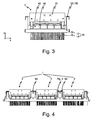
- Fig. 2 and 3 show the power converter assembly in two different two-dimensional views.
- Fig. 4 shows a power converter arrangement according to the invention.
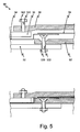
- Fig. 5 shows in a partial view the connection of two power converter modules of a power converter arrangement according to the invention.
- Fig. 1 shows as part of a converter arrangement according to the invention (1) a power converter module (2) with a cooling device (10), a plurality of power semiconductor modules (40) and a capacitor device (20) in three-dimensional view.
- the cooling device (10 which is formed here as a base plate (12) with a coolant (14), here in the form of fins of an air cooling device.
- a liquid cooling is conceivable, which allows a higher electrical power of the power converter module (2), in the range of one megawatt, due to the higher cooling capacity.
- the cooling means (14) for reasons of cooling efficiency below the Power semiconductor modules (40).
- an expansion over the entire area of the baseplate (12) may be advantageous in order to further increase the cooling capacity.
- the capacitor device (20) is also arranged on the base plate (12) of the cooling device (10) and in turn consists of a plurality of similar capacitors (200).
- the capacitor device (20) is immediately adjacent to the DC connection elements (42, 44, cf. Fig. 2 ) of the power semiconductor modules (40).
- the combined arrangement of the power semiconductor components (40) and the capacitor device (20) on the cooling device (10) results in a very compact and mechanically stable unit of the power converter module (2).
- the power semiconductor modules (40) themselves each have a half-bridge circuit and are connected in parallel with one another in order to achieve the desired power of the power converter module (2).
- the cooling device (10) facing away from the drive circuit (80) is arranged in a separate sub-housing. This arrangement achieved by their short paths for the control signals a particularly high noise immunity against external noise.
- This busbar (30) consists of a first (32) and a second (36) metal moldings with an insulating intermediate layer (34).
- the respective metal moldings (32, 36) have individual tabs for connection to the DC connection elements (42, 44).
- the metal moldings (32, 36) of the busbar (30) are formed flat.
- the flat metal shaped bodies (32, 36) of the busbar (30) project beyond the condenser unit (20) in both orientations. Necessary here is only an overlap in the direction of a next to be arranged power converter module, here the y-direction.
- the first metal shaped body (32) of the busbar (30) connects the negative DC voltage connection elements (42) of the power semiconductor components (40) in a polarity-compatible manner with the associated connection elements of the capacitors (200) of the capacitor device (20).
- the second metal shaped body (36) connects the positive DC voltage connection elements (44) of the power semiconductor modules (40) in a polarity-compatible manner with the associated connection elements of the capacitors (200) of the capacitor device (20).
- the first metal shaped body (32) has recesses, through which the connecting elements of the capacitors (200) extend in an insulated manner.
- the first metal shaped body (32) has, in its edge regions which overlap the capacitor device (20), screw receptacles (50) which are connected to the first connection means to the low-inductance high-current carrying connection (90, cf. Fig. 4 ) of this power converter module (2) to an adjacent power converter module and in Fig. 5 are described in detail.
- the second metal shaped body (36) has, close to two of its edge areas, a plurality of threaded studs (60) which, with the second connecting means (360, 362), form the low-inductance high-current carrying connection (90) of this power converter module (2) to an adjacent power converter module Fig. 5 are described in detail.
- Fig. 2 and 3 show the power converter module (2) according to Fig. 1 in two different two-dimensional views.
- Fig. 2 Both the planar busbar (30) and the screw receptacles (50) of the first metal shaped body (32) of the busbar (30) and the threaded pin (60) of the second metal shaped body (36) of the busbar (30) are clearly visible.
- the direct current connections (42, 44) of the power semiconductor modules (40) and the associated tabs of the metal shaped bodies (32, 36) of the busbar (30) can be seen here.
- Fig. 3 clearly shows the cooling device (10) with the base plate (12) and the cooling fins (14) as a coolant.
- the power semiconductor modules (40) are arranged on this base plate (12). These are connected on the one hand, the AC power connection element (70) as well as the busbar (30) to the capacitor device (20). Shown is also the screw receptacle (50) of the first metal shaped body (32).
- Fig. 4 shows a power converter arrangement (1) according to the invention. This has three power converter modules (2) which have a connection (90) to each other. For this purpose, the busbars (30) which contact the capacitors (200) of the capacitor device (20) of the respective power converter module (2) are connected to one another.
- this connection (90) serves the uniform load distribution to the three capacitor devices (20).
- Essential for this is the low-inductive compound and high current carrying capacity of the compound produced (90).
- Fig. 5 shows in a partial view the connection (90) of two power converter assemblies (2) of a power converter arrangement according to the invention additionally by means of an exploded view. Shown is the busbar (30), each having a first (32) and a second (36) metal moldings, and an interposed insulating intermediate layer (34).
- a first connecting means For connecting the first metal shaped body (32), a first connecting means is provided.
- the first metal shaped body (32) has a recess and on the side facing the capacitor device a screw receptacle (320).
- a first connecting body (92) is provided which also has a recess for receiving a screw (322).
- This first connecting body (92) is arranged in such a way to the first metal shaped body (32) that the two recesses are aligned with each other.
- the screw (322) By arranging the screw (322), a non-positive electrically conductive connection between the first metal shaped body (32) and the first connecting body (92) is produced. Since the first connecting body (92) advantageously has the same length (y-direction) as the first metal shaped body (32), an electrical connection of high current-carrying capacity thus arises.
- a second connecting means For connecting the second metal shaped body (36) a second connecting means is provided.
- the second metal molded body (36) has a threaded pin (360).
- a two connecting body (96) is provided which has a recess for receiving this threaded pin (360).
- the second metal shaped body (36) is frictionally connected to the second connecting body (96) by arranging a nut (362) on the threaded pin (360). Since the second connecting body (96) advantageously the same length (y-direction) as the second metal moldings (36) also this compound has a high current carrying capacity. By forming this connection, the second (36) connector body completely covers the first (32).
- connection (90) of two power converter modules (2) ensures their current-carrying capacity.
- the low-inductive connection is ensured by the fact that the respective distance is minimal both continuously between the metal moldings (32, 36), between the connecting bodies (92, 96) and also in the transition region between metal moldings and connecting bodies.
- connection (90) according to the invention of two power converter modules (2) is that it is accessible for simple production, since in a sequential method only the first connecting device subsequently the associated further insulating intermediate layer (94) and subsequently the second connecting device are arranged can. It is also essential here that all these production steps can be carried out from the side facing away from the condenser device.
Landscapes
- Engineering & Computer Science (AREA)
- Microelectronics & Electronic Packaging (AREA)
- Physics & Mathematics (AREA)
- Thermal Sciences (AREA)
- Power Engineering (AREA)
- Inverter Devices (AREA)
- Dc-Dc Converters (AREA)
Claims (6)
- Dispositif de convertisseur (1), avec :une pluralité de groupes de convertisseur (2) ayant chacun un dispositif de refroidissement (10), au moins un module semi-conducteur de puissance (40) disposé sur celui-ci, et avec un dispositif de condensateur (20), qui lui est relié par circuit adapté, par groupe de convertisseur (2),l'au moins un module semi-conducteur de puissance (40) étant disposé de manière étroitement contiguë au dispositif de condensateur (20), et des éléments de connexion de charge à courant continu (42, 44) du module semi-conducteur de puissance (40) étant reliés au dispositif de condensateur (20) au moyen d'une barre (30) réalisée avec une forme plate, ladite barre (30) plate étant constituée d'un premier (32) et d'un deuxième (36) corps moulé métallique avec un intercalaire (34) isolant et recouvrant le dispositif de condensateur (20) dans au moins une direction, et les barres (30) de deux groupes de convertisseur (2) contigus pouvant être reliées l'une à l'autre à faible inductance en connectant le premier corps moulé métallique (32) au moyen d'un premier corps de connexion (92) plat et de premiers moyens de connexion (320, 322), en connectant le deuxième corps moulé métallique (36) au moyen d'un deuxième corps de connexion (96) plat et de deuxièmes moyens de connexion (360, 362), le premier corps de connexion (92) étant recouvert par le deuxième corps de connexion (96),un autre intercalaire (94) isolant étant disposé entre les deux corps de connexion (92, 96),le premier moyen de connexion (320, 322) étant réalisé comme connexion filetée mécanique, le premier corps moulé métallique (32) comportant un logement de vis (50) et le premier corps de connexion (92) un évidement pour la réception d'une vis (322) de la connexion filetée, et l'assemblage mécanique étant obtenu par disposition de la vis (322) dans l'évidement ainsi que dans le logement de vis (320), etle deuxième moyen de connexion (360, 362) étant réalisé comme connexion filetée mécanique, le deuxième corps moulé métallique (36) comportant une goupille filetée (360) et le deuxième corps de connexion (96) un évidement pour le passage de ladite goupille filetée (360), et l'assemblage mécanique étant obtenu par disposition d'un écrou (362) sur la goupille filetée (360).
- Dispositif de convertisseur selon la revendication 1, dans lequel le dispositif de condensateur (20) comporte une pluralité de condensateurs (200) comprenant des éléments de connexion qui sont reliés en fonction de la polarité au premier (32) ou au deuxième (36) corps moulé métallique respectivement associé de la barre (30).
- Dispositif de convertisseur selon la revendication 1, dans lequel le premier corps moulé métallique (32) présente des évidements pour le passage isolé d'éléments de connexion de polarités différenciées des condensateurs (200) du dispositif de condensateur (20).
- Dispositif de convertisseur selon la revendication 1, dans lequel le dispositif de condensateur (20) est disposé sur le dispositif de refroidissement (10).
- Dispositif de convertisseur selon la revendication 1, dans lequel un élément de connexion à courant alternatif (70) de l'au moins un module semi-conducteur de puissance (40) est disposé sur le côté du module semi-conducteur de puissance (40) distant du dispositif de condensateur (20).
- Dispositif de convertisseur selon la revendication 1, dans lequel un circuit de commande (80) est disposé sur le côté de l'au moins un module semi-conducteur de puissance (40) d'un groupe de convertisseur (2) distant du dispositif de refroidissement (10).
Applications Claiming Priority (1)
| Application Number | Priority Date | Filing Date | Title |
|---|---|---|---|
| DE102009043181A DE102009043181A1 (de) | 2009-09-26 | 2009-09-26 | Stromrichteranordnung |
Publications (2)
| Publication Number | Publication Date |
|---|---|
| EP2302782A1 EP2302782A1 (fr) | 2011-03-30 |
| EP2302782B1 true EP2302782B1 (fr) | 2013-04-03 |
Family
ID=43428565
Family Applications (1)
| Application Number | Title | Priority Date | Filing Date |
|---|---|---|---|
| EP10170744A Active EP2302782B1 (fr) | 2009-09-26 | 2010-07-26 | Agencement de convertisseur de courant |
Country Status (4)
| Country | Link |
|---|---|
| EP (1) | EP2302782B1 (fr) |
| CN (1) | CN102035356B (fr) |
| DE (1) | DE102009043181A1 (fr) |
| ES (1) | ES2407643T3 (fr) |
Families Citing this family (13)
| Publication number | Priority date | Publication date | Assignee | Title |
|---|---|---|---|---|
| EP2574157A1 (fr) * | 2011-09-23 | 2013-03-27 | AEG Power Solutions B.V. | Composant électronique de puissance et agencement comprenant au moins un tel composant électronique de puissance |
| DE102013103866B3 (de) * | 2013-04-17 | 2014-05-22 | Semikron Elektronik Gmbh & Co. Kg | Leistungshalbleitereinrichtung |
| EP2814308B1 (fr) * | 2013-06-10 | 2019-06-26 | SEMIKRON Elektronik GmbH & Co. KG | Dispositif convertisseur de courant à 3 niveaux |
| DE102014104308B3 (de) * | 2014-03-27 | 2015-07-02 | Semikron Elektronik Gmbh & Co. Kg | Leistungshalbleitereinrichtungssystem |
| DE102014213784A1 (de) * | 2014-07-16 | 2016-01-21 | Siemens Aktiengesellschaft | Umrichter |
| EP2986092B1 (fr) * | 2014-08-12 | 2017-10-11 | SEMIKRON Elektronik GmbH & Co. KG | Armoire pour convertisseur de puissance |
| CN104779484A (zh) * | 2015-05-06 | 2015-07-15 | 南车株洲电力机车研究所有限公司 | 一种变流器模块连接装置 |
| WO2018095552A1 (fr) * | 2016-11-28 | 2018-05-31 | Siemens Aktiengesellschaft | Convertisseur |
| DE102017109706B3 (de) | 2017-05-05 | 2018-03-08 | Semikron Elektronik Gmbh & Co. Kg | Leistungselektronische Anordnung mit Gleichspannungsverbindungselement |
| DE102019134791A1 (de) * | 2019-12-17 | 2021-06-17 | Valeo Siemens Eautomotive Germany Gmbh | Elektrische Vorrichtung für einen Stromrichter, Stromrichter und Anordnung mit einer elektrischen Maschine und einem Stromrichter |
| DE102020111574B3 (de) | 2020-04-28 | 2021-07-22 | Semikron Elektronik Gmbh & Co. Kg | Leistungselektronische Anordnung mit Gleichspannungsverbindungselement und Verfahren zur Herstellung |
| DE102020111573B4 (de) | 2020-04-28 | 2023-09-14 | Semikron Elektronik Gmbh & Co. Kg | Leistungselektronische Anordnung mit Gleichspannungsverbindungselement und Verfahren zur Herstellung |
| CN120730619B (zh) * | 2025-08-13 | 2025-11-21 | 浙江晶科储能有限公司 | 储能变流器、储能系统和用电设备 |
Citations (1)
| Publication number | Priority date | Publication date | Assignee | Title |
|---|---|---|---|---|
| EP2015626A2 (fr) * | 2007-06-22 | 2009-01-14 | Hitachi Ltd. | Structure d'un convertisseur de puissance |
Family Cites Families (9)
| Publication number | Priority date | Publication date | Assignee | Title |
|---|---|---|---|---|
| ATE127272T1 (de) * | 1990-04-05 | 1995-09-15 | Siemens Matsushita Components | Kondensatorbatterie mit niederinduktiver verschaltung. |
| DE19832225C2 (de) | 1998-07-17 | 2003-03-20 | Semikron Elektronik Gmbh | Vierquadrantenumrichter für mittlere und höhere Spannungen |
| JP3724345B2 (ja) * | 2000-07-13 | 2005-12-07 | 日産自動車株式会社 | 配線の接続部構造 |
| JP3906440B2 (ja) * | 2000-09-06 | 2007-04-18 | 株式会社日立製作所 | 半導体電力変換装置 |
| DE10153748A1 (de) * | 2001-10-31 | 2003-05-22 | Siemens Ag | Stromrichtereinheit in Modulbauweise |
| US7248483B2 (en) * | 2004-08-19 | 2007-07-24 | Xantrex Technology, Inc. | High power density insulated metal substrate based power converter assembly with very low BUS impedance |
| FR2878368B1 (fr) * | 2004-11-22 | 2007-01-12 | Semikron Sarl | Systeme de connexion entre batteries de condensateurs |
| DK1815486T3 (da) * | 2004-11-22 | 2012-07-09 | Semikron Elektronik Gmbh | Forbindelsessystem imellem kondensatorbatterier |
| JP4756935B2 (ja) * | 2005-06-29 | 2011-08-24 | 本田技研工業株式会社 | コンデンサ搭載型インバータユニット |
-
2009
- 2009-09-26 DE DE102009043181A patent/DE102009043181A1/de not_active Withdrawn
-
2010
- 2010-07-26 ES ES10170744T patent/ES2407643T3/es active Active
- 2010-07-26 EP EP10170744A patent/EP2302782B1/fr active Active
- 2010-09-21 CN CN201010295672.1A patent/CN102035356B/zh active Active
Patent Citations (1)
| Publication number | Priority date | Publication date | Assignee | Title |
|---|---|---|---|---|
| EP2015626A2 (fr) * | 2007-06-22 | 2009-01-14 | Hitachi Ltd. | Structure d'un convertisseur de puissance |
Also Published As
| Publication number | Publication date |
|---|---|
| CN102035356A (zh) | 2011-04-27 |
| CN102035356B (zh) | 2014-09-24 |
| EP2302782A1 (fr) | 2011-03-30 |
| DE102009043181A1 (de) | 2011-04-07 |
| ES2407643T3 (es) | 2013-06-13 |
Similar Documents
| Publication | Publication Date | Title |
|---|---|---|
| EP2302782B1 (fr) | Agencement de convertisseur de courant | |
| DE102017115883B4 (de) | Leistungselektronisches Submodul mit Gleich- und Wechselspannungsanschlusselementen und Anordnung hiermit | |
| DE102010000082B4 (de) | Schaltungsanordnung von elektronischen Leistungsschaltern einer Stromerzeugungsvorrichtung | |
| DE102017109706B3 (de) | Leistungselektronische Anordnung mit Gleichspannungsverbindungselement | |
| DE102018104972B4 (de) | Leiterplattenelement mit integriertem elektronischen Schaltelement, Stromrichter und Verfahren zum Herstellen eines Leiterplattenelements | |
| DE102020206199A1 (de) | Stromrichter | |
| WO2021111004A1 (fr) | Onduleur ayant une conception compacte | |
| DE102016004884B4 (de) | Antriebssystem mit einer Zwischenkreisverschienung | |
| EP3180850B1 (fr) | Circuit faiblement inductif d'un convertisseur | |
| DE102020006207A1 (de) | Motorantriebsvorrichtung mit Glättungskondensatoreinheit und Beschaltungskondensator | |
| WO2014184030A1 (fr) | Dispositif et module électrique permettant de convertir une tension continue en tension alternative | |
| DE10107839A1 (de) | Anordnung mit einem auf einem Träger montierten integrierten Schaltkreis und einer Stromversorgungsbaugruppenanordnung | |
| WO2015062901A1 (fr) | Système à condensateur et procédé de fonctionnement d'un système à condensateur | |
| DE102017127895A1 (de) | Wechselrichter für Elektromotor | |
| DE102021119379B4 (de) | Anordnung mit einem Leistungswandler und mit einer Gleichspannungs-Stromschiene zum elektrischen Anschluss an einen Gleichspannungs-Zwischenkreis des Leistungswandlers sowie modulares System | |
| EP3834591B1 (fr) | Agencement de circuit intermédiaire et onduleur | |
| DE102019115498B4 (de) | Leistungselektronisches Submodul mit Gleich- und Wechselpotentialanschlussflächen und Anordnung hiermit | |
| DE102018000961A1 (de) | Elektronische Anordnung mit Leistungsmodul, Leiterplatte und Kühlkörper | |
| DE102019110716B3 (de) | Leistungshalbleitermodul mit Leistungshalbleiterschaltern | |
| DE102024127006B3 (de) | Leistungshalbleitermodul mit einem ersten und einem zweiten Gleichspannungs-Lastanschluss | |
| DE102025104540B3 (de) | Leistungselektronische Schaltungsanordnung sowie Stromrichter | |
| EP3945572A1 (fr) | Module de semi-conducteur de puissance et procédé de fabrication d'un module de semi-conducteur de puissance | |
| DE102009024384B4 (de) | Leistungshalbleitermodul in gestapelter Bauweise | |
| DE102024200742B4 (de) | Sammelschienensystem | |
| DE102019009143B4 (de) | Leistungselektronisches Submodul mit Gleich- und Wechselpotentialanschlussflächen |
Legal Events
| Date | Code | Title | Description |
|---|---|---|---|
| PUAI | Public reference made under article 153(3) epc to a published international application that has entered the european phase |
Free format text: ORIGINAL CODE: 0009012 |
|
| 17P | Request for examination filed |
Effective date: 20100902 |
|
| AK | Designated contracting states |
Kind code of ref document: A1 Designated state(s): AL AT BE BG CH CY CZ DE DK EE ES FI FR GB GR HR HU IE IS IT LI LT LU LV MC MK MT NL NO PL PT RO SE SI SK SM TR |
|
| AX | Request for extension of the european patent |
Extension state: BA ME RS |
|
| RIC1 | Information provided on ipc code assigned before grant |
Ipc: H02M 7/00 20060101AFI20121129BHEP |
|
| GRAP | Despatch of communication of intention to grant a patent |
Free format text: ORIGINAL CODE: EPIDOSNIGR1 |
|
| GRAS | Grant fee paid |
Free format text: ORIGINAL CODE: EPIDOSNIGR3 |
|
| GRAA | (expected) grant |
Free format text: ORIGINAL CODE: 0009210 |
|
| AK | Designated contracting states |
Kind code of ref document: B1 Designated state(s): AL AT BE BG CH CY CZ DE DK EE ES FI FR GB GR HR HU IE IS IT LI LT LU LV MC MK MT NL NO PL PT RO SE SI SK SM TR |
|
| REG | Reference to a national code |
Ref country code: GB Ref legal event code: FG4D Free format text: NOT ENGLISH |
|
| REG | Reference to a national code |
Ref country code: AT Ref legal event code: REF Ref document number: 605254 Country of ref document: AT Kind code of ref document: T Effective date: 20130415 Ref country code: CH Ref legal event code: EP |
|
| REG | Reference to a national code |
Ref country code: IE Ref legal event code: FG4D Free format text: LANGUAGE OF EP DOCUMENT: GERMAN |
|
| REG | Reference to a national code |
Ref country code: DE Ref legal event code: R096 Ref document number: 502010002752 Country of ref document: DE Effective date: 20130529 |
|
| REG | Reference to a national code |
Ref country code: ES Ref legal event code: FG2A Ref document number: 2407643 Country of ref document: ES Kind code of ref document: T3 Effective date: 20130613 |
|
| PG25 | Lapsed in a contracting state [announced via postgrant information from national office to epo] |
Ref country code: SI Free format text: LAPSE BECAUSE OF FAILURE TO SUBMIT A TRANSLATION OF THE DESCRIPTION OR TO PAY THE FEE WITHIN THE PRESCRIBED TIME-LIMIT Effective date: 20130403 |
|
| REG | Reference to a national code |
Ref country code: NL Ref legal event code: VDEP Effective date: 20130403 |
|
| REG | Reference to a national code |
Ref country code: LT Ref legal event code: MG4D |
|
| PG25 | Lapsed in a contracting state [announced via postgrant information from national office to epo] |
Ref country code: GR Free format text: LAPSE BECAUSE OF FAILURE TO SUBMIT A TRANSLATION OF THE DESCRIPTION OR TO PAY THE FEE WITHIN THE PRESCRIBED TIME-LIMIT Effective date: 20130704 Ref country code: IS Free format text: LAPSE BECAUSE OF FAILURE TO SUBMIT A TRANSLATION OF THE DESCRIPTION OR TO PAY THE FEE WITHIN THE PRESCRIBED TIME-LIMIT Effective date: 20130803 Ref country code: SE Free format text: LAPSE BECAUSE OF FAILURE TO SUBMIT A TRANSLATION OF THE DESCRIPTION OR TO PAY THE FEE WITHIN THE PRESCRIBED TIME-LIMIT Effective date: 20130403 Ref country code: FI Free format text: LAPSE BECAUSE OF FAILURE TO SUBMIT A TRANSLATION OF THE DESCRIPTION OR TO PAY THE FEE WITHIN THE PRESCRIBED TIME-LIMIT Effective date: 20130403 Ref country code: NO Free format text: LAPSE BECAUSE OF FAILURE TO SUBMIT A TRANSLATION OF THE DESCRIPTION OR TO PAY THE FEE WITHIN THE PRESCRIBED TIME-LIMIT Effective date: 20130703 Ref country code: LT Free format text: LAPSE BECAUSE OF FAILURE TO SUBMIT A TRANSLATION OF THE DESCRIPTION OR TO PAY THE FEE WITHIN THE PRESCRIBED TIME-LIMIT Effective date: 20130403 Ref country code: NL Free format text: LAPSE BECAUSE OF FAILURE TO SUBMIT A TRANSLATION OF THE DESCRIPTION OR TO PAY THE FEE WITHIN THE PRESCRIBED TIME-LIMIT Effective date: 20130403 Ref country code: PT Free format text: LAPSE BECAUSE OF FAILURE TO SUBMIT A TRANSLATION OF THE DESCRIPTION OR TO PAY THE FEE WITHIN THE PRESCRIBED TIME-LIMIT Effective date: 20130805 |
|
| PG25 | Lapsed in a contracting state [announced via postgrant information from national office to epo] |
Ref country code: BG Free format text: LAPSE BECAUSE OF FAILURE TO SUBMIT A TRANSLATION OF THE DESCRIPTION OR TO PAY THE FEE WITHIN THE PRESCRIBED TIME-LIMIT Effective date: 20130703 Ref country code: LV Free format text: LAPSE BECAUSE OF FAILURE TO SUBMIT A TRANSLATION OF THE DESCRIPTION OR TO PAY THE FEE WITHIN THE PRESCRIBED TIME-LIMIT Effective date: 20130403 Ref country code: CY Free format text: LAPSE BECAUSE OF FAILURE TO SUBMIT A TRANSLATION OF THE DESCRIPTION OR TO PAY THE FEE WITHIN THE PRESCRIBED TIME-LIMIT Effective date: 20130403 Ref country code: PL Free format text: LAPSE BECAUSE OF FAILURE TO SUBMIT A TRANSLATION OF THE DESCRIPTION OR TO PAY THE FEE WITHIN THE PRESCRIBED TIME-LIMIT Effective date: 20130403 Ref country code: HR Free format text: LAPSE BECAUSE OF FAILURE TO SUBMIT A TRANSLATION OF THE DESCRIPTION OR TO PAY THE FEE WITHIN THE PRESCRIBED TIME-LIMIT Effective date: 20130403 |
|
| BERE | Be: lapsed |
Owner name: SEMIKRON ELEKTRONIK G.M.B.H. & CO. KG Effective date: 20130731 |
|
| PG25 | Lapsed in a contracting state [announced via postgrant information from national office to epo] |
Ref country code: DK Free format text: LAPSE BECAUSE OF FAILURE TO SUBMIT A TRANSLATION OF THE DESCRIPTION OR TO PAY THE FEE WITHIN THE PRESCRIBED TIME-LIMIT Effective date: 20130403 Ref country code: CZ Free format text: LAPSE BECAUSE OF FAILURE TO SUBMIT A TRANSLATION OF THE DESCRIPTION OR TO PAY THE FEE WITHIN THE PRESCRIBED TIME-LIMIT Effective date: 20130403 Ref country code: EE Free format text: LAPSE BECAUSE OF FAILURE TO SUBMIT A TRANSLATION OF THE DESCRIPTION OR TO PAY THE FEE WITHIN THE PRESCRIBED TIME-LIMIT Effective date: 20130403 Ref country code: SK Free format text: LAPSE BECAUSE OF FAILURE TO SUBMIT A TRANSLATION OF THE DESCRIPTION OR TO PAY THE FEE WITHIN THE PRESCRIBED TIME-LIMIT Effective date: 20130403 |
|
| PLBE | No opposition filed within time limit |
Free format text: ORIGINAL CODE: 0009261 |
|
| STAA | Information on the status of an ep patent application or granted ep patent |
Free format text: STATUS: NO OPPOSITION FILED WITHIN TIME LIMIT |
|
| PG25 | Lapsed in a contracting state [announced via postgrant information from national office to epo] |
Ref country code: RO Free format text: LAPSE BECAUSE OF FAILURE TO SUBMIT A TRANSLATION OF THE DESCRIPTION OR TO PAY THE FEE WITHIN THE PRESCRIBED TIME-LIMIT Effective date: 20130403 Ref country code: MC Free format text: LAPSE BECAUSE OF FAILURE TO SUBMIT A TRANSLATION OF THE DESCRIPTION OR TO PAY THE FEE WITHIN THE PRESCRIBED TIME-LIMIT Effective date: 20130403 |
|
| 26N | No opposition filed |
Effective date: 20140106 |
|
| REG | Reference to a national code |
Ref country code: DE Ref legal event code: R097 Ref document number: 502010002752 Country of ref document: DE Effective date: 20140106 |
|
| REG | Reference to a national code |
Ref country code: IE Ref legal event code: MM4A |
|
| PG25 | Lapsed in a contracting state [announced via postgrant information from national office to epo] |
Ref country code: BE Free format text: LAPSE BECAUSE OF NON-PAYMENT OF DUE FEES Effective date: 20130731 |
|
| PG25 | Lapsed in a contracting state [announced via postgrant information from national office to epo] |
Ref country code: IE Free format text: LAPSE BECAUSE OF NON-PAYMENT OF DUE FEES Effective date: 20130726 |
|
| REG | Reference to a national code |
Ref country code: CH Ref legal event code: PL |
|
| PG25 | Lapsed in a contracting state [announced via postgrant information from national office to epo] |
Ref country code: LI Free format text: LAPSE BECAUSE OF NON-PAYMENT OF DUE FEES Effective date: 20140731 Ref country code: CH Free format text: LAPSE BECAUSE OF NON-PAYMENT OF DUE FEES Effective date: 20140731 |
|
| PG25 | Lapsed in a contracting state [announced via postgrant information from national office to epo] |
Ref country code: SM Free format text: LAPSE BECAUSE OF FAILURE TO SUBMIT A TRANSLATION OF THE DESCRIPTION OR TO PAY THE FEE WITHIN THE PRESCRIBED TIME-LIMIT Effective date: 20130403 |
|
| PG25 | Lapsed in a contracting state [announced via postgrant information from national office to epo] |
Ref country code: TR Free format text: LAPSE BECAUSE OF FAILURE TO SUBMIT A TRANSLATION OF THE DESCRIPTION OR TO PAY THE FEE WITHIN THE PRESCRIBED TIME-LIMIT Effective date: 20130403 Ref country code: MT Free format text: LAPSE BECAUSE OF FAILURE TO SUBMIT A TRANSLATION OF THE DESCRIPTION OR TO PAY THE FEE WITHIN THE PRESCRIBED TIME-LIMIT Effective date: 20130403 |
|
| PG25 | Lapsed in a contracting state [announced via postgrant information from national office to epo] |
Ref country code: HU Free format text: LAPSE BECAUSE OF FAILURE TO SUBMIT A TRANSLATION OF THE DESCRIPTION OR TO PAY THE FEE WITHIN THE PRESCRIBED TIME-LIMIT; INVALID AB INITIO Effective date: 20100726 Ref country code: MK Free format text: LAPSE BECAUSE OF FAILURE TO SUBMIT A TRANSLATION OF THE DESCRIPTION OR TO PAY THE FEE WITHIN THE PRESCRIBED TIME-LIMIT Effective date: 20130403 Ref country code: LU Free format text: LAPSE BECAUSE OF NON-PAYMENT OF DUE FEES Effective date: 20130726 |
|
| REG | Reference to a national code |
Ref country code: FR Ref legal event code: PLFP Year of fee payment: 7 |
|
| REG | Reference to a national code |
Ref country code: AT Ref legal event code: MM01 Ref document number: 605254 Country of ref document: AT Kind code of ref document: T Effective date: 20150726 |
|
| PG25 | Lapsed in a contracting state [announced via postgrant information from national office to epo] |
Ref country code: AT Free format text: LAPSE BECAUSE OF NON-PAYMENT OF DUE FEES Effective date: 20150726 |
|
| REG | Reference to a national code |
Ref country code: FR Ref legal event code: PLFP Year of fee payment: 8 |
|
| REG | Reference to a national code |
Ref country code: FR Ref legal event code: PLFP Year of fee payment: 9 |
|
| PG25 | Lapsed in a contracting state [announced via postgrant information from national office to epo] |
Ref country code: AL Free format text: LAPSE BECAUSE OF FAILURE TO SUBMIT A TRANSLATION OF THE DESCRIPTION OR TO PAY THE FEE WITHIN THE PRESCRIBED TIME-LIMIT Effective date: 20130403 |
|
| PGFP | Annual fee paid to national office [announced via postgrant information from national office to epo] |
Ref country code: GB Payment date: 20250605 Year of fee payment: 16 |
|
| PGFP | Annual fee paid to national office [announced via postgrant information from national office to epo] |
Ref country code: FR Payment date: 20250610 Year of fee payment: 16 |
|
| PGFP | Annual fee paid to national office [announced via postgrant information from national office to epo] |
Ref country code: ES Payment date: 20250806 Year of fee payment: 16 |
|
| PGFP | Annual fee paid to national office [announced via postgrant information from national office to epo] |
Ref country code: DE Payment date: 20250604 Year of fee payment: 16 |
|
| REG | Reference to a national code |
Ref country code: DE Ref legal event code: R081 Ref document number: 502010002752 Country of ref document: DE Owner name: SEMIKRON DANFOSS ELEKTRONIK GMBH & CO. KG, DE Free format text: FORMER OWNER: SEMIKRON ELEKTRONIK GMBH & CO. KG, 90431 NUERNBERG, DE |
|
| PGFP | Annual fee paid to national office [announced via postgrant information from national office to epo] |
Ref country code: IT Payment date: 20250623 Year of fee payment: 16 |