EP2306067B1 - Module de source lumineuse - Google Patents
Module de source lumineuse Download PDFInfo
- Publication number
- EP2306067B1 EP2306067B1 EP10162837.8A EP10162837A EP2306067B1 EP 2306067 B1 EP2306067 B1 EP 2306067B1 EP 10162837 A EP10162837 A EP 10162837A EP 2306067 B1 EP2306067 B1 EP 2306067B1
- Authority
- EP
- European Patent Office
- Prior art keywords
- heat dissipation
- dissipation block
- light emitting
- emitting diode
- light source
- Prior art date
- Legal status (The legal status is an assumption and is not a legal conclusion. Google has not performed a legal analysis and makes no representation as to the accuracy of the status listed.)
- Not-in-force
Links
- 230000017525 heat dissipation Effects 0.000 claims description 56
- 229910000679 solder Inorganic materials 0.000 claims description 9
- PXHVJJICTQNCMI-UHFFFAOYSA-N Nickel Chemical compound [Ni] PXHVJJICTQNCMI-UHFFFAOYSA-N 0.000 description 4
- 239000000463 material Substances 0.000 description 4
- 238000005516 engineering process Methods 0.000 description 2
- 238000005286 illumination Methods 0.000 description 2
- 229910052759 nickel Inorganic materials 0.000 description 2
- 230000003247 decreasing effect Effects 0.000 description 1
- 230000000694 effects Effects 0.000 description 1
- 238000005562 fading Methods 0.000 description 1
- 238000004519 manufacturing process Methods 0.000 description 1
- 239000004065 semiconductor Substances 0.000 description 1
- 238000005476 soldering Methods 0.000 description 1
- 239000002470 thermal conductor Substances 0.000 description 1
Images



Classifications
-
- F—MECHANICAL ENGINEERING; LIGHTING; HEATING; WEAPONS; BLASTING
- F21—LIGHTING
- F21V—FUNCTIONAL FEATURES OR DETAILS OF LIGHTING DEVICES OR SYSTEMS THEREOF; STRUCTURAL COMBINATIONS OF LIGHTING DEVICES WITH OTHER ARTICLES, NOT OTHERWISE PROVIDED FOR
- F21V29/00—Protecting lighting devices from thermal damage; Cooling or heating arrangements specially adapted for lighting devices or systems
- F21V29/50—Cooling arrangements
- F21V29/70—Cooling arrangements characterised by passive heat-dissipating elements, e.g. heat-sinks
- F21V29/74—Cooling arrangements characterised by passive heat-dissipating elements, e.g. heat-sinks with fins or blades
- F21V29/77—Cooling arrangements characterised by passive heat-dissipating elements, e.g. heat-sinks with fins or blades with essentially identical diverging planar fins or blades, e.g. with fan-like or star-like cross-section
-
- F—MECHANICAL ENGINEERING; LIGHTING; HEATING; WEAPONS; BLASTING
- F21—LIGHTING
- F21V—FUNCTIONAL FEATURES OR DETAILS OF LIGHTING DEVICES OR SYSTEMS THEREOF; STRUCTURAL COMBINATIONS OF LIGHTING DEVICES WITH OTHER ARTICLES, NOT OTHERWISE PROVIDED FOR
- F21V23/00—Arrangement of electric circuit elements in or on lighting devices
- F21V23/02—Arrangement of electric circuit elements in or on lighting devices the elements being transformers, impedances or power supply units, e.g. a transformer with a rectifier
-
- F—MECHANICAL ENGINEERING; LIGHTING; HEATING; WEAPONS; BLASTING
- F21—LIGHTING
- F21K—NON-ELECTRIC LIGHT SOURCES USING LUMINESCENCE; LIGHT SOURCES USING ELECTROCHEMILUMINESCENCE; LIGHT SOURCES USING CHARGES OF COMBUSTIBLE MATERIAL; LIGHT SOURCES USING SEMICONDUCTOR DEVICES AS LIGHT-GENERATING ELEMENTS; LIGHT SOURCES NOT OTHERWISE PROVIDED FOR
- F21K9/00—Light sources using semiconductor devices as light-generating elements, e.g. using light-emitting diodes [LED] or lasers
- F21K9/20—Light sources comprising attachment means
- F21K9/23—Retrofit light sources for lighting devices with a single fitting for each light source, e.g. for substitution of incandescent lamps with bayonet or threaded fittings
-
- F—MECHANICAL ENGINEERING; LIGHTING; HEATING; WEAPONS; BLASTING
- F21—LIGHTING
- F21V—FUNCTIONAL FEATURES OR DETAILS OF LIGHTING DEVICES OR SYSTEMS THEREOF; STRUCTURAL COMBINATIONS OF LIGHTING DEVICES WITH OTHER ARTICLES, NOT OTHERWISE PROVIDED FOR
- F21V29/00—Protecting lighting devices from thermal damage; Cooling or heating arrangements specially adapted for lighting devices or systems
- F21V29/50—Cooling arrangements
- F21V29/60—Cooling arrangements characterised by the use of a forced flow of gas, e.g. air
- F21V29/67—Cooling arrangements characterised by the use of a forced flow of gas, e.g. air characterised by the arrangement of fans
- F21V29/677—Cooling arrangements characterised by the use of a forced flow of gas, e.g. air characterised by the arrangement of fans the fans being used for discharging
-
- F—MECHANICAL ENGINEERING; LIGHTING; HEATING; WEAPONS; BLASTING
- F21—LIGHTING
- F21V—FUNCTIONAL FEATURES OR DETAILS OF LIGHTING DEVICES OR SYSTEMS THEREOF; STRUCTURAL COMBINATIONS OF LIGHTING DEVICES WITH OTHER ARTICLES, NOT OTHERWISE PROVIDED FOR
- F21V29/00—Protecting lighting devices from thermal damage; Cooling or heating arrangements specially adapted for lighting devices or systems
- F21V29/50—Cooling arrangements
- F21V29/70—Cooling arrangements characterised by passive heat-dissipating elements, e.g. heat-sinks
- F21V29/74—Cooling arrangements characterised by passive heat-dissipating elements, e.g. heat-sinks with fins or blades
-
- F—MECHANICAL ENGINEERING; LIGHTING; HEATING; WEAPONS; BLASTING
- F21—LIGHTING
- F21V—FUNCTIONAL FEATURES OR DETAILS OF LIGHTING DEVICES OR SYSTEMS THEREOF; STRUCTURAL COMBINATIONS OF LIGHTING DEVICES WITH OTHER ARTICLES, NOT OTHERWISE PROVIDED FOR
- F21V29/00—Protecting lighting devices from thermal damage; Cooling or heating arrangements specially adapted for lighting devices or systems
- F21V29/50—Cooling arrangements
- F21V29/502—Cooling arrangements characterised by the adaptation for cooling of specific components
- F21V29/507—Cooling arrangements characterised by the adaptation for cooling of specific components of means for protecting lighting devices from damage, e.g. housings
-
- F—MECHANICAL ENGINEERING; LIGHTING; HEATING; WEAPONS; BLASTING
- F21—LIGHTING
- F21V—FUNCTIONAL FEATURES OR DETAILS OF LIGHTING DEVICES OR SYSTEMS THEREOF; STRUCTURAL COMBINATIONS OF LIGHTING DEVICES WITH OTHER ARTICLES, NOT OTHERWISE PROVIDED FOR
- F21V29/00—Protecting lighting devices from thermal damage; Cooling or heating arrangements specially adapted for lighting devices or systems
- F21V29/50—Cooling arrangements
- F21V29/70—Cooling arrangements characterised by passive heat-dissipating elements, e.g. heat-sinks
- F21V29/83—Cooling arrangements characterised by passive heat-dissipating elements, e.g. heat-sinks the elements having apertures, ducts or channels, e.g. heat radiation holes
-
- F—MECHANICAL ENGINEERING; LIGHTING; HEATING; WEAPONS; BLASTING
- F21—LIGHTING
- F21Y—INDEXING SCHEME ASSOCIATED WITH SUBCLASSES F21K, F21L, F21S and F21V, RELATING TO THE FORM OR THE KIND OF THE LIGHT SOURCES OR OF THE COLOUR OF THE LIGHT EMITTED
- F21Y2115/00—Light-generating elements of semiconductor light sources
- F21Y2115/10—Light-emitting diodes [LED]
Definitions
- the present invention relates to a light source module, and more particularly to a light source module with a light emitting diode package used as a light emitting device.
- LED current light emitting diodes
- the LED when the LED emits light with high luminance, it generates high thermal energy. If the thermal energy cannot be transmitted away and keeps on accumulating within the LED, the temperature of the LED is continuously increased. Therefore, the over heated LED leads to the luminance of the LED fading away and the decreasing of the lifetime of the LED and even the permanent damage of the LED. Hence, the current illumination using the LED is equipped with a heat sink to dissipate the heat generated by the LED.
- the LED is disposed on the circuit board and the circuit board having the LED thereon is disposed on the heat sink.
- the heat conducted onto the heat sink from the LED is conducted away through the air current generated by the fan.
- the circuit board usually has the insulating layers thereon to insulate the wire layers from each other, and the insulating layers are poor thermal conductors. Therefore, the thermal conducting rate of conducting the heat of the LED to the heat sink through the circuit board is seriously affected and the heat dissipation efficiency of the LED light source module is poor.
- the present invention provides a light source module having a relatively better heat dissipation efficiency.
- a light source module including a heat dissipation block, a light emitting diode package, a circuit board, and a fan module.
- the heat dissipation block has a surface and the light emitting diode package is disposed on the surface of the heat dissipation block.
- the circuit board is electrically connected to the light emitting diode package, and the circuit board and the light emitting diode package are disposed at two opposite sides of the heat dissipation block respectively.
- the fan module is disposed between the heat dissipation block and the circuit board.
- the fan module has an opening, a blade and a baffle plate circling the opening. The blade is disposed in the opening for generating an air current which flows along a flowing direction to dissipate the heat of the heat dissipation block.
- the baffle plate prevents the air current from flowing along a direction opposite to the flowing direction.
- the light source module further comprises at least a conductive device electrically connected to the light emitting diode package and the circuit board.
- the heat dissipation block has a recess for disposing the light emitting diode package therein, and the conductive device penetrates through the heat dissipation block, and the light emitting diode package is electrically connected to one end of the conductive device.
- the light source module further comprises at least an insulating ring circling the conductive device and electrically insulating the conductive device from the heat dissipation block.
- the conductive device is a conductive pillar.
- One end of the conductive pillar away from the light emitting diode package protrudes from the insulating ring and has a protruding edge, and a radius of an outer periphery of the protruding edge is larger than a radius of an inner periphery of the insulating ring.
- the light source module further comprises at least a conductive line, and one end of the conductive line winds between the insulating ring and the protruding edge, and the other end of the conductive line is connected to the circuit board.
- the heat dissipation block has a solder point.
- the light emitting diode package is configured on the heat dissipation block by being soldered on the solder point.
- the light source module further comprises a lamp cup, wherein the fan module and the heat dissipation block are configured on the lamp cup, and the heat dissipation block is configured on the fan module.
- the light source module of the embodiment of the present invention since the light emitting diode package is configured on the surface of the heat dissipation block, the heat generated by the light emitting diode package can be directly conducted to the heat dissipation block without being blocked by the circuit board. Therefore, the light source module of the embodiment of the present invention possesses a relatively better heat dissipation efficiency. Moreover, in the light source module of the embodiment of the present invention, because the fan module has the baffle plate to prevent the air current from flowing along a direction opposite to the flow direction of the air current in the opening and to further improve the heat convection, the light source module possesses a relatively better heat dissipation efficiency.
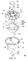
- Fig. 1 is a schematic view of a light source module according to one embodiment of the present invention.
- Fig. 2 is an exploded view of the light source module in Fig. 1 .
- a light source module 100 of the present embodiment includes a heat dissipation block 110 and a light emitting diode package 120.
- the heat dissipation block 110 has a surface 112 and the light emitting diode package 120 is disposed on the surface 112 of the heat dissipation block 110.
- the light source module 100 further comprises a circuit board 130 electrically connected to the light emitting diode package 120 and a fan module 140.
- the light emitting diode package 120 and the circuit board 130 are disposed on two opposite sides of the heat dissipation block 110 respectively and the fan module 140 is disposed between the heat dissipation block 110 and the circuit board 130.
- the fan module 140 has an opening 142 and a blade 144 disposed in the opening 142.
- the blade 144 is adapted to generate an air current.
- the air current in the opening 142 flows along a flowing direction A1 to dissipate the heat of the heat dissipation block 110.
- the heat generated by the light emitting diode package 120 on the surface 112 of the heat dissipation block 110 can be carried away by the air current to avoid the light emitting diode package 120 from being over heated.
- the light emitting efficiency and the lifetime of the light emitting diode package 120 can be improved.
- the fan module 140 of the present invention has a baffle plate 146 circling the opening 142.
- the baffle plate 146 can prevent the air current from flowing along a direction opposite to the flowing direction Al so as to keep the thermal air contact with the heat dissipation block 110 from flowing back and to further improve the heat convection. Therefore, the light source module 100 of the present embodiment has better heat dissipation efficiency.
- the heat dissipation block 110 can have a solder point 116.
- the material of the heat dissipation block 110 can be, for example but not limited to, solder material.
- the material of the solder point 116 can be, for example, nickel.
- the light emitting diode package 120 can be configured on the heat dissipation block 110 by being soldered on the solder point 116, and nickel is adapted to soldering with the solder material.
- the light emitting diode package 120 can combine with the heat dissipation block 110 by using the surface mount technology (SMT) to enhance a manufacturing efficiency of the light source module 100.
- SMT surface mount technology
- Fig. 3 is a schematic enlarged view showing the conductive device of FIG. 1 equipped with the light emitting diode package.
- the light source module 100 further comprises two conductive devices 150, two insulating rings 160 and two conductive lines 190.
- the conductive devices 150 can be, for example, conductive pillars electrically connected to the light emitting diode package 120 and the circuit board 130.
- the heat dissipation block 110 has a recess 114 for disposing the light emitting diode package 120 therein, and the conductive devices 150 penetrate through the heat dissipation block 110, and the light emitting diode package 120 is electrically connected to one end of each of the conductive devices 150.
- the insulating ring 160 circles the corresponding conductive device 150 respectively so as to electrically insulate the conductive devices 150 from the heat dissipation block 110.
- the other end of each of the conductive devices 150 which is far away from the light emitting diode package 120, protrudes from the insulating ring 160 and has a protruding edge 152.
- the radius of the outer periphery of each protruding edge 152 is larger than the radius of the inner periphery of each insulating ring 160 so that one end of the conductive lines 190 can securely wind between the insulating rings 160 and the protruding edges 152 without easily falling off.
- the baffle plate 146 has a through hole 146a formed by indenting a portion of the outer periphery of the baffle plate 146.
- One end of each conductive line 190 winds between the insulating ring 160 and the protruding edge 152, and the other end of each conductive line 190 passes through the through hole 146a and is connected to the circuit board 130 so that the light emitting diode package 120 is electrically connect to the circuit board.
- Fig. 4 is a schematic view of the lamp cup in the light source module of Fig. 1 before the lamp cup is assembled.
- Fig. 5 is a schematic view of the lamp cup in the light source module of Fig. 1 after the lamp cup is assembled.
- the light source module 100 further comprises a lamp cup 170 and a connector 180 fixed on the lamp cup 170, and the connector 180 is electrically connected to the circuit board 130 in the lamp cup 170.
- the fan module 140 and the heat dissipation block 110 are configured on the lamp cup 170, and the heat dissipation block 110 is configured on the fan module 140.
- the fan module 140 and the heat dissipation block 110 can be, for example, locked on the lamp cup 170.
- the lamp cup 170 can have a plurality of assembling holes 172.
- a plurality of fixing pieces 174 can pass through the assembling holes 172 respectively to lock the lamp cup 170 and the fan module 140 on the heat dissipation block 110.
- the lamp cup 170 can have a slot 176.
- the connector 180 can be buckled in the slot 176 so that the connector 180 can be stably configured in the lamp cup 170.
- the light source module of the embodiment of the present invention since the light emitting diode package is configured on the surface of the heat dissipation block, the heat generated by the light emitting diode package can be directly conducted to the heat dissipation block without being blocked by the circuit board. Therefore, the light source module of the embodiment of the present invention possesses a relatively better heat dissipation efficiency. Moreover, in the light source module of the embodiment of the present invention, because the fan module has the baffle plate to prevent the air current from flowing along a direction opposite to the flow direction of the air current in the opening and to further improve the heat convection, the light source module possesses a relatively better heat dissipation efficiency.
Landscapes
- Engineering & Computer Science (AREA)
- General Engineering & Computer Science (AREA)
- Power Engineering (AREA)
- Physics & Mathematics (AREA)
- Microelectronics & Electronic Packaging (AREA)
- Optics & Photonics (AREA)
- Led Device Packages (AREA)
- Arrangement Of Elements, Cooling, Sealing, Or The Like Of Lighting Devices (AREA)
- Non-Portable Lighting Devices Or Systems Thereof (AREA)
- Cooling Or The Like Of Semiconductors Or Solid State Devices (AREA)
Claims (6)
- Module à source lumineuse (100), comprenant :un bloc de dissipation de chaleur (110) possédant une surface (112) ;un boîtier de diode électroluminescente (120) disposé sur la surface (112) du bloc de dissipation de chaleur (110) ;une carte de circuit imprimé (130) connectée électriquement au boîtier de diode électroluminescente (120), dans lequel la carte de circuit imprimé (130) et le boîtier de diode électroluminescente (120) sont disposés sur deux côtés opposés du bloc de dissipation de chaleur (110) respectivement ; etun module à ventilateur (140), dans lequel le module à ventilateur (140) est disposé entre le bloc de dissipation de chaleur (110) et la carte de circuit imprimé (130),caractérisé en ce que le module à ventilateur (140) comporte une ouverture (142), une pale (144) et une plaque déflectrice (146) encerclant l'ouverture (142), la pale (144) étant disposée dans l'ouverture (142) pour produire un courant d'air qui s'écoule le long d'une direction d'écoulement (A1) pour dissiper la chaleur du bloc de dissipation de chaleur (110), et la plaque déflectrice (146) empêchant le courant d'air de s'écouler le long d'une direction opposée à la direction d'écoulement (A1).
- Module à source lumineuse (100) selon la revendication 1, comprenant en outre au moins un dispositif conducteur (150) connecté électriquement au boîtier de diode électroluminescente (120) et à la carte de circuit imprimé (130), et le bloc de dissipation de chaleur (110) comporte un évidement (114) pour disposer le boîtier de diode électroluminescente (120) dans celui-ci, le dispositif conducteur (150) pénètre à travers le bloc de dissipation de chaleur (110), et le boîtier de diode électroluminescente (120) est connecté électriquement à une extrémité du dispositif conducteur (150).
- Module à source lumineuse (100) selon la revendication 2, comprenant en outre au moins une bague isolante encerclant le dispositif conducteur (150) et isolant électriquement le dispositif conducteur (150) par rapport au bloc de dissipation de chaleur (110), dans lequel le dispositif conducteur (150) est un pilier conducteur, et une extrémité du pilier éloignée du boîtier de diode électroluminescente (120) fait saillie à partir de la bague isolante (160) et comporte un bord saillant (152), et un rayon d'une périphérie extérieure du bord saillant (152) est supérieur à un rayon d'une périphérie intérieure de la bague isolante (160).
- Module à source lumineuse (100) selon la revendication 3, comprenant en outre au moins une ligne conductrice (190), et une extrémité de la ligne conductrice (190) s'enroule entre la bague isolante (160) et le bord saillant (152), et l'autre extrémité de la ligne conductrice (190) est connectée à la carte de circuit imprimé (130).
- Module à source lumineuse (100) selon la revendication 1, dans lequel le bloc de dissipation de chaleur (110) comporte un point de brasure (116), et le boîtier de diode électroluminescente (120) est configuré sur le bloc de dissipation de chaleur (110) en étant brasé sur le point de brasure (116).
- Module à source lumineuse (100) selon la revendication 1, comprenant en outre une coupelle de lampe (170), dans lequel le module à ventilateur (140) et le bloc de dissipation de chaleur (110) sont configurés sur la coupelle de lampe (170), et le bloc de dissipation de chaleur (110) est configuré sur le module à ventilateur (140).
Applications Claiming Priority (1)
| Application Number | Priority Date | Filing Date | Title |
|---|---|---|---|
| TW098133262A TWI373592B (en) | 2009-09-30 | 2009-09-30 | Light source module |
Publications (3)
| Publication Number | Publication Date |
|---|---|
| EP2306067A2 EP2306067A2 (fr) | 2011-04-06 |
| EP2306067A3 EP2306067A3 (fr) | 2012-04-11 |
| EP2306067B1 true EP2306067B1 (fr) | 2014-07-30 |
Family
ID=43558484
Family Applications (1)
| Application Number | Title | Priority Date | Filing Date |
|---|---|---|---|
| EP10162837.8A Not-in-force EP2306067B1 (fr) | 2009-09-30 | 2010-05-14 | Module de source lumineuse |
Country Status (3)
| Country | Link |
|---|---|
| US (1) | US8125125B2 (fr) |
| EP (1) | EP2306067B1 (fr) |
| TW (1) | TWI373592B (fr) |
Families Citing this family (5)
| Publication number | Priority date | Publication date | Assignee | Title |
|---|---|---|---|---|
| US9383084B2 (en) | 2010-06-21 | 2016-07-05 | Light Emitting Design, Inc. | Mounting system for an industrial light |
| US8272765B2 (en) | 2010-06-21 | 2012-09-25 | Light Emitting Design, Inc. | Heat sink system |
| KR101227522B1 (ko) * | 2011-05-25 | 2013-01-31 | 엘지전자 주식회사 | 조명 장치 |
| JP2013077579A (ja) * | 2013-01-17 | 2013-04-25 | Sharp Corp | 照明装置 |
| JP6781553B2 (ja) * | 2015-03-25 | 2020-11-04 | エルジー イノテック カンパニー リミテッド | ホルダーおよびこれを具備する照明装置 |
Family Cites Families (15)
| Publication number | Priority date | Publication date | Assignee | Title |
|---|---|---|---|---|
| JP2959121B2 (ja) | 1990-11-28 | 1999-10-06 | 三菱瓦斯化学株式会社 | メタクリル酸の製造法 |
| US5573992A (en) | 1994-10-28 | 1996-11-12 | E. I. Du Pont De Nemours And Company | Process for the calcination/activation of V/P/O catalyst |
| TW290777B (en) | 1996-04-20 | 1996-11-11 | United Microelectronics Corp | Video compression digital signal decoder and decoding method thereof |
| WO2007005827A2 (fr) * | 2005-07-01 | 2007-01-11 | Little Giant Pump Company | Appareil adaptateur de montage pour del |
| TWM294616U (en) | 2006-01-26 | 2006-07-21 | Litmx Inc | Improved lamp structure |
| TWI290777B (en) | 2006-02-27 | 2007-12-01 | Guei-Fang Chen | Lighting device with light emitting diode |
| TW200825324A (en) | 2006-12-01 | 2008-06-16 | gui-fang Chen | Heat dissipating lamp housing and illuminating module comprising the same |
| CN201028447Y (zh) | 2007-01-06 | 2008-02-27 | 宁波艾里根斯电器有限公司 | Led照明灯 |
| TWM337673U (en) | 2007-07-06 | 2008-08-01 | Lustrous Technology Ltd | An LED lamp and an LED packaging structure therein |
| CN101368719B (zh) * | 2007-08-13 | 2011-07-06 | 太一节能系统股份有限公司 | 发光二极管灯具 |
| CN201110529Y (zh) | 2007-10-15 | 2008-09-03 | 协禧电机股份有限公司 | 具风扇散热功用的发光二极管灯 |
| TWM330426U (en) | 2007-11-05 | 2008-04-11 | Unity Opto Technology Co Ltd | Heat dissipation structure of lamp |
| CN101532646B (zh) * | 2008-03-14 | 2012-06-13 | 富准精密工业(深圳)有限公司 | 照明装置 |
| TWM342472U (en) * | 2008-04-22 | 2008-10-11 | Fin Core Corp | LED lighting device |
| CN101672432B (zh) * | 2008-09-11 | 2012-11-21 | 富准精密工业(深圳)有限公司 | 发光二极管灯具 |
-
2009
- 2009-09-30 TW TW098133262A patent/TWI373592B/zh not_active IP Right Cessation
-
2010
- 2010-05-07 US US12/775,478 patent/US8125125B2/en not_active Expired - Fee Related
- 2010-05-14 EP EP10162837.8A patent/EP2306067B1/fr not_active Not-in-force
Also Published As
| Publication number | Publication date |
|---|---|
| TW201111694A (en) | 2011-04-01 |
| TWI373592B (en) | 2012-10-01 |
| US8125125B2 (en) | 2012-02-28 |
| US20110074268A1 (en) | 2011-03-31 |
| EP2306067A2 (fr) | 2011-04-06 |
| EP2306067A3 (fr) | 2012-04-11 |
Similar Documents
| Publication | Publication Date | Title |
|---|---|---|
| JP5101578B2 (ja) | 発光ダイオード照明装置 | |
| US8262256B2 (en) | Semiconductor light module | |
| KR101713059B1 (ko) | 발광소자 조명 장치 | |
| JP6052573B2 (ja) | 光半導体光源及び車両用照明装置 | |
| US20120268941A1 (en) | Light Emitting Diode Lamp and Assembling Method Thereof | |
| JP2006295085A (ja) | 発光ダイオード光源ユニット | |
| EP2306067B1 (fr) | Module de source lumineuse | |
| CN102213371B (zh) | 灯具结构 | |
| US20180062059A1 (en) | Light-emitting module, lighting apparatus for mobile object, and mobile object | |
| JP5705323B2 (ja) | 放熱特性が向上した高光力led光源構造体 | |
| US20090218586A1 (en) | Led lamp | |
| JP5873598B2 (ja) | Ledランプ用電極モジュール | |
| KR20140113617A (ko) | 발광 소자 모듈 | |
| KR101276326B1 (ko) | 비아홀을 갖는 인쇄회로기판, 이를 구비한 엘이디 모듈 및 led 조명장치 | |
| KR20140122474A (ko) | 엘이디조명 조립체 | |
| KR20090102208A (ko) | 방열 led 패키지 | |
| US20140009934A1 (en) | Illuminating device and method of fabricating the illuminating device | |
| US20150123559A1 (en) | Optical semiconductor lighting apparatus | |
| CN102042494B (zh) | 光源模组 | |
| KR101278835B1 (ko) | 엘이디용 회로기판원판, 회로기판, 엘이디유닛, 조명기구 및 제조방법 | |
| KR200416346Y1 (ko) | 고출력 led 램프 장착용 인쇄회로기판 모듈 및 이를이용한 조명용 led 램프 모듈 | |
| KR101469215B1 (ko) | 피부 치료용 led모듈 | |
| CN102155636A (zh) | 光源模组与散热块 | |
| KR20140065493A (ko) | 램프용 pcb 기판 및 이를 포함하는 램프 | |
| TWI416041B (zh) | 燈具結構 |
Legal Events
| Date | Code | Title | Description |
|---|---|---|---|
| PUAI | Public reference made under article 153(3) epc to a published international application that has entered the european phase |
Free format text: ORIGINAL CODE: 0009012 |
|
| AK | Designated contracting states |
Kind code of ref document: A2 Designated state(s): AL AT BE BG CH CY CZ DE DK EE ES FI FR GB GR HR HU IE IS IT LI LT LU LV MC MK MT NL NO PL PT RO SE SI SK SM TR |
|
| AX | Request for extension of the european patent |
Extension state: BA ME RS |
|
| PUAL | Search report despatched |
Free format text: ORIGINAL CODE: 0009013 |
|
| AK | Designated contracting states |
Kind code of ref document: A3 Designated state(s): AL AT BE BG CH CY CZ DE DK EE ES FI FR GB GR HR HU IE IS IT LI LT LU LV MC MK MT NL NO PL PT RO SE SI SK SM TR |
|
| AX | Request for extension of the european patent |
Extension state: BA ME RS |
|
| RIC1 | Information provided on ipc code assigned before grant |
Ipc: F21Y 101/02 20060101ALN20120308BHEP Ipc: F21V 29/02 20060101ALI20120308BHEP Ipc: F21V 29/00 20060101ALI20120308BHEP Ipc: F21K 99/00 20100101AFI20120308BHEP |
|
| 17P | Request for examination filed |
Effective date: 20121010 |
|
| 17Q | First examination report despatched |
Effective date: 20130807 |
|
| GRAP | Despatch of communication of intention to grant a patent |
Free format text: ORIGINAL CODE: EPIDOSNIGR1 |
|
| INTG | Intention to grant announced |
Effective date: 20140314 |
|
| GRAS | Grant fee paid |
Free format text: ORIGINAL CODE: EPIDOSNIGR3 |
|
| GRAA | (expected) grant |
Free format text: ORIGINAL CODE: 0009210 |
|
| AK | Designated contracting states |
Kind code of ref document: B1 Designated state(s): AL AT BE BG CH CY CZ DE DK EE ES FI FR GB GR HR HU IE IS IT LI LT LU LV MC MK MT NL NO PL PT RO SE SI SK SM TR |
|
| REG | Reference to a national code |
Ref country code: GB Ref legal event code: FG4D |
|
| REG | Reference to a national code |
Ref country code: CH Ref legal event code: EP |
|
| REG | Reference to a national code |
Ref country code: AT Ref legal event code: REF Ref document number: 680160 Country of ref document: AT Kind code of ref document: T Effective date: 20140815 |
|
| REG | Reference to a national code |
Ref country code: IE Ref legal event code: FG4D |
|
| REG | Reference to a national code |
Ref country code: DE Ref legal event code: R096 Ref document number: 602010017844 Country of ref document: DE Effective date: 20140911 |
|
| REG | Reference to a national code |
Ref country code: AT Ref legal event code: MK05 Ref document number: 680160 Country of ref document: AT Kind code of ref document: T Effective date: 20140730 |
|
| REG | Reference to a national code |
Ref country code: NL Ref legal event code: VDEP Effective date: 20140730 |
|
| REG | Reference to a national code |
Ref country code: LT Ref legal event code: MG4D |
|
| PG25 | Lapsed in a contracting state [announced via postgrant information from national office to epo] |
Ref country code: BG Free format text: LAPSE BECAUSE OF FAILURE TO SUBMIT A TRANSLATION OF THE DESCRIPTION OR TO PAY THE FEE WITHIN THE PRESCRIBED TIME-LIMIT Effective date: 20141030 Ref country code: LT Free format text: LAPSE BECAUSE OF FAILURE TO SUBMIT A TRANSLATION OF THE DESCRIPTION OR TO PAY THE FEE WITHIN THE PRESCRIBED TIME-LIMIT Effective date: 20140730 Ref country code: GR Free format text: LAPSE BECAUSE OF FAILURE TO SUBMIT A TRANSLATION OF THE DESCRIPTION OR TO PAY THE FEE WITHIN THE PRESCRIBED TIME-LIMIT Effective date: 20141031 Ref country code: FI Free format text: LAPSE BECAUSE OF FAILURE TO SUBMIT A TRANSLATION OF THE DESCRIPTION OR TO PAY THE FEE WITHIN THE PRESCRIBED TIME-LIMIT Effective date: 20140730 Ref country code: ES Free format text: LAPSE BECAUSE OF FAILURE TO SUBMIT A TRANSLATION OF THE DESCRIPTION OR TO PAY THE FEE WITHIN THE PRESCRIBED TIME-LIMIT Effective date: 20140730 Ref country code: PT Free format text: LAPSE BECAUSE OF FAILURE TO SUBMIT A TRANSLATION OF THE DESCRIPTION OR TO PAY THE FEE WITHIN THE PRESCRIBED TIME-LIMIT Effective date: 20141202 Ref country code: NO Free format text: LAPSE BECAUSE OF FAILURE TO SUBMIT A TRANSLATION OF THE DESCRIPTION OR TO PAY THE FEE WITHIN THE PRESCRIBED TIME-LIMIT Effective date: 20141030 Ref country code: SE Free format text: LAPSE BECAUSE OF FAILURE TO SUBMIT A TRANSLATION OF THE DESCRIPTION OR TO PAY THE FEE WITHIN THE PRESCRIBED TIME-LIMIT Effective date: 20140730 |
|
| PG25 | Lapsed in a contracting state [announced via postgrant information from national office to epo] |
Ref country code: AT Free format text: LAPSE BECAUSE OF FAILURE TO SUBMIT A TRANSLATION OF THE DESCRIPTION OR TO PAY THE FEE WITHIN THE PRESCRIBED TIME-LIMIT Effective date: 20140730 Ref country code: CY Free format text: LAPSE BECAUSE OF FAILURE TO SUBMIT A TRANSLATION OF THE DESCRIPTION OR TO PAY THE FEE WITHIN THE PRESCRIBED TIME-LIMIT Effective date: 20140730 Ref country code: HR Free format text: LAPSE BECAUSE OF FAILURE TO SUBMIT A TRANSLATION OF THE DESCRIPTION OR TO PAY THE FEE WITHIN THE PRESCRIBED TIME-LIMIT Effective date: 20140730 Ref country code: LV Free format text: LAPSE BECAUSE OF FAILURE TO SUBMIT A TRANSLATION OF THE DESCRIPTION OR TO PAY THE FEE WITHIN THE PRESCRIBED TIME-LIMIT Effective date: 20140730 Ref country code: PL Free format text: LAPSE BECAUSE OF FAILURE TO SUBMIT A TRANSLATION OF THE DESCRIPTION OR TO PAY THE FEE WITHIN THE PRESCRIBED TIME-LIMIT Effective date: 20140730 Ref country code: IS Free format text: LAPSE BECAUSE OF FAILURE TO SUBMIT A TRANSLATION OF THE DESCRIPTION OR TO PAY THE FEE WITHIN THE PRESCRIBED TIME-LIMIT Effective date: 20141130 Ref country code: NL Free format text: LAPSE BECAUSE OF FAILURE TO SUBMIT A TRANSLATION OF THE DESCRIPTION OR TO PAY THE FEE WITHIN THE PRESCRIBED TIME-LIMIT Effective date: 20140730 |
|
| PG25 | Lapsed in a contracting state [announced via postgrant information from national office to epo] |
Ref country code: EE Free format text: LAPSE BECAUSE OF FAILURE TO SUBMIT A TRANSLATION OF THE DESCRIPTION OR TO PAY THE FEE WITHIN THE PRESCRIBED TIME-LIMIT Effective date: 20140730 Ref country code: SK Free format text: LAPSE BECAUSE OF FAILURE TO SUBMIT A TRANSLATION OF THE DESCRIPTION OR TO PAY THE FEE WITHIN THE PRESCRIBED TIME-LIMIT Effective date: 20140730 Ref country code: IT Free format text: LAPSE BECAUSE OF FAILURE TO SUBMIT A TRANSLATION OF THE DESCRIPTION OR TO PAY THE FEE WITHIN THE PRESCRIBED TIME-LIMIT Effective date: 20140730 Ref country code: CZ Free format text: LAPSE BECAUSE OF FAILURE TO SUBMIT A TRANSLATION OF THE DESCRIPTION OR TO PAY THE FEE WITHIN THE PRESCRIBED TIME-LIMIT Effective date: 20140730 Ref country code: DK Free format text: LAPSE BECAUSE OF FAILURE TO SUBMIT A TRANSLATION OF THE DESCRIPTION OR TO PAY THE FEE WITHIN THE PRESCRIBED TIME-LIMIT Effective date: 20140730 Ref country code: RO Free format text: LAPSE BECAUSE OF FAILURE TO SUBMIT A TRANSLATION OF THE DESCRIPTION OR TO PAY THE FEE WITHIN THE PRESCRIBED TIME-LIMIT Effective date: 20140730 |
|
| REG | Reference to a national code |
Ref country code: DE Ref legal event code: R097 Ref document number: 602010017844 Country of ref document: DE |
|
| PLBE | No opposition filed within time limit |
Free format text: ORIGINAL CODE: 0009261 |
|
| STAA | Information on the status of an ep patent application or granted ep patent |
Free format text: STATUS: NO OPPOSITION FILED WITHIN TIME LIMIT |
|
| 26N | No opposition filed |
Effective date: 20150504 |
|
| PG25 | Lapsed in a contracting state [announced via postgrant information from national office to epo] |
Ref country code: SI Free format text: LAPSE BECAUSE OF FAILURE TO SUBMIT A TRANSLATION OF THE DESCRIPTION OR TO PAY THE FEE WITHIN THE PRESCRIBED TIME-LIMIT Effective date: 20140730 |
|
| REG | Reference to a national code |
Ref country code: CH Ref legal event code: PL |
|
| GBPC | Gb: european patent ceased through non-payment of renewal fee |
Effective date: 20150514 |
|
| PG25 | Lapsed in a contracting state [announced via postgrant information from national office to epo] |
Ref country code: CH Free format text: LAPSE BECAUSE OF NON-PAYMENT OF DUE FEES Effective date: 20150531 Ref country code: LU Free format text: LAPSE BECAUSE OF FAILURE TO SUBMIT A TRANSLATION OF THE DESCRIPTION OR TO PAY THE FEE WITHIN THE PRESCRIBED TIME-LIMIT Effective date: 20150514 Ref country code: LI Free format text: LAPSE BECAUSE OF NON-PAYMENT OF DUE FEES Effective date: 20150531 Ref country code: MC Free format text: LAPSE BECAUSE OF FAILURE TO SUBMIT A TRANSLATION OF THE DESCRIPTION OR TO PAY THE FEE WITHIN THE PRESCRIBED TIME-LIMIT Effective date: 20140730 |
|
| REG | Reference to a national code |
Ref country code: IE Ref legal event code: MM4A |
|
| REG | Reference to a national code |
Ref country code: FR Ref legal event code: ST Effective date: 20160129 |
|
| PG25 | Lapsed in a contracting state [announced via postgrant information from national office to epo] |
Ref country code: GB Free format text: LAPSE BECAUSE OF NON-PAYMENT OF DUE FEES Effective date: 20150514 Ref country code: IE Free format text: LAPSE BECAUSE OF NON-PAYMENT OF DUE FEES Effective date: 20150514 |
|
| PG25 | Lapsed in a contracting state [announced via postgrant information from national office to epo] |
Ref country code: FR Free format text: LAPSE BECAUSE OF NON-PAYMENT OF DUE FEES Effective date: 20150601 |
|
| PG25 | Lapsed in a contracting state [announced via postgrant information from national office to epo] |
Ref country code: BE Free format text: LAPSE BECAUSE OF FAILURE TO SUBMIT A TRANSLATION OF THE DESCRIPTION OR TO PAY THE FEE WITHIN THE PRESCRIBED TIME-LIMIT Effective date: 20140730 |
|
| PG25 | Lapsed in a contracting state [announced via postgrant information from national office to epo] |
Ref country code: MT Free format text: LAPSE BECAUSE OF FAILURE TO SUBMIT A TRANSLATION OF THE DESCRIPTION OR TO PAY THE FEE WITHIN THE PRESCRIBED TIME-LIMIT Effective date: 20140730 |
|
| PG25 | Lapsed in a contracting state [announced via postgrant information from national office to epo] |
Ref country code: HU Free format text: LAPSE BECAUSE OF FAILURE TO SUBMIT A TRANSLATION OF THE DESCRIPTION OR TO PAY THE FEE WITHIN THE PRESCRIBED TIME-LIMIT; INVALID AB INITIO Effective date: 20100514 Ref country code: SM Free format text: LAPSE BECAUSE OF FAILURE TO SUBMIT A TRANSLATION OF THE DESCRIPTION OR TO PAY THE FEE WITHIN THE PRESCRIBED TIME-LIMIT Effective date: 20140730 |
|
| PG25 | Lapsed in a contracting state [announced via postgrant information from national office to epo] |
Ref country code: TR Free format text: LAPSE BECAUSE OF FAILURE TO SUBMIT A TRANSLATION OF THE DESCRIPTION OR TO PAY THE FEE WITHIN THE PRESCRIBED TIME-LIMIT Effective date: 20140730 |
|
| PG25 | Lapsed in a contracting state [announced via postgrant information from national office to epo] |
Ref country code: MK Free format text: LAPSE BECAUSE OF FAILURE TO SUBMIT A TRANSLATION OF THE DESCRIPTION OR TO PAY THE FEE WITHIN THE PRESCRIBED TIME-LIMIT Effective date: 20140730 |
|
| PGFP | Annual fee paid to national office [announced via postgrant information from national office to epo] |
Ref country code: DE Payment date: 20180529 Year of fee payment: 9 |
|
| PG25 | Lapsed in a contracting state [announced via postgrant information from national office to epo] |
Ref country code: AL Free format text: LAPSE BECAUSE OF FAILURE TO SUBMIT A TRANSLATION OF THE DESCRIPTION OR TO PAY THE FEE WITHIN THE PRESCRIBED TIME-LIMIT Effective date: 20140730 |
|
| RIC2 | Information provided on ipc code assigned after grant |
Ipc: F21K 99/00 20160101AFI20120308BHEP Ipc: F21V 29/02 20060101ALI20120308BHEP Ipc: F21Y 101/02 20000101ALN20120308BHEP Ipc: F21V 29/00 20150101ALI20120308BHEP |
|
| REG | Reference to a national code |
Ref country code: DE Ref legal event code: R119 Ref document number: 602010017844 Country of ref document: DE |
|
| PG25 | Lapsed in a contracting state [announced via postgrant information from national office to epo] |
Ref country code: DE Free format text: LAPSE BECAUSE OF NON-PAYMENT OF DUE FEES Effective date: 20191203 |