EP2306496A2 - Procédé et dispositif pour enlever un composant collé sur un film souple - Google Patents
Procédé et dispositif pour enlever un composant collé sur un film souple Download PDFInfo
- Publication number
- EP2306496A2 EP2306496A2 EP10186245A EP10186245A EP2306496A2 EP 2306496 A2 EP2306496 A2 EP 2306496A2 EP 10186245 A EP10186245 A EP 10186245A EP 10186245 A EP10186245 A EP 10186245A EP 2306496 A2 EP2306496 A2 EP 2306496A2
- Authority
- EP
- European Patent Office
- Prior art keywords
- film
- support
- component
- plane
- support plane
- Prior art date
- Legal status (The legal status is an assumption and is not a legal conclusion. Google has not performed a legal analysis and makes no representation as to the accuracy of the status listed.)
- Withdrawn
Links
Images


Classifications
-
- H—ELECTRICITY
- H10—SEMICONDUCTOR DEVICES; ELECTRIC SOLID-STATE DEVICES NOT OTHERWISE PROVIDED FOR
- H10P—GENERIC PROCESSES OR APPARATUS FOR THE MANUFACTURE OR TREATMENT OF DEVICES COVERED BY CLASS H10
- H10P95/00—Generic processes or apparatus for manufacture or treatments not covered by the other groups of this subclass
-
- H—ELECTRICITY
- H10—SEMICONDUCTOR DEVICES; ELECTRIC SOLID-STATE DEVICES NOT OTHERWISE PROVIDED FOR
- H10P—GENERIC PROCESSES OR APPARATUS FOR THE MANUFACTURE OR TREATMENT OF DEVICES COVERED BY CLASS H10
- H10P72/00—Handling or holding of wafers, substrates or devices during manufacture or treatment thereof
- H10P72/04—Apparatus for manufacture or treatment
- H10P72/0442—Apparatus for placing on an insulating substrate, e.g. tape
-
- Y—GENERAL TAGGING OF NEW TECHNOLOGICAL DEVELOPMENTS; GENERAL TAGGING OF CROSS-SECTIONAL TECHNOLOGIES SPANNING OVER SEVERAL SECTIONS OF THE IPC; TECHNICAL SUBJECTS COVERED BY FORMER USPC CROSS-REFERENCE ART COLLECTIONS [XRACs] AND DIGESTS
- Y10—TECHNICAL SUBJECTS COVERED BY FORMER USPC
- Y10S—TECHNICAL SUBJECTS COVERED BY FORMER USPC CROSS-REFERENCE ART COLLECTIONS [XRACs] AND DIGESTS
- Y10S438/00—Semiconductor device manufacturing: process
- Y10S438/976—Temporary protective layer
-
- Y—GENERAL TAGGING OF NEW TECHNOLOGICAL DEVELOPMENTS; GENERAL TAGGING OF CROSS-SECTIONAL TECHNOLOGIES SPANNING OVER SEVERAL SECTIONS OF THE IPC; TECHNICAL SUBJECTS COVERED BY FORMER USPC CROSS-REFERENCE ART COLLECTIONS [XRACs] AND DIGESTS
- Y10—TECHNICAL SUBJECTS COVERED BY FORMER USPC
- Y10T—TECHNICAL SUBJECTS COVERED BY FORMER US CLASSIFICATION
- Y10T156/00—Adhesive bonding and miscellaneous chemical manufacture
- Y10T156/11—Methods of delaminating, per se; i.e., separating at bonding face
- Y10T156/1126—Using direct fluid current against work during delaminating
- Y10T156/1132—Using vacuum directly against work during delaminating
-
- Y—GENERAL TAGGING OF NEW TECHNOLOGICAL DEVELOPMENTS; GENERAL TAGGING OF CROSS-SECTIONAL TECHNOLOGIES SPANNING OVER SEVERAL SECTIONS OF THE IPC; TECHNICAL SUBJECTS COVERED BY FORMER USPC CROSS-REFERENCE ART COLLECTIONS [XRACs] AND DIGESTS
- Y10—TECHNICAL SUBJECTS COVERED BY FORMER USPC
- Y10T—TECHNICAL SUBJECTS COVERED BY FORMER US CLASSIFICATION
- Y10T156/00—Adhesive bonding and miscellaneous chemical manufacture
- Y10T156/19—Delaminating means
- Y10T156/1928—Differential fluid pressure delaminating means
- Y10T156/1944—Vacuum delaminating means [e.g., vacuum chamber, etc.]
Definitions
- the invention relates to a device for detaching a component bonded to a flexible film according to the description in paragraphs [0057] to [0066]. Namely, in the processing of semiconductor chips, such devices are used to remove a plurality of chips from the wafer foil in rapid succession and place them on a support.
- the semiconductor chips with the electronic circuits arranged thereon are previously singulated by sawing from the silicon wafer called wafer.
- the wafer is glued to the wafer film stretched in a frame, where it must be evident that the adhesion must be sufficiently high to prevent breakouts or chip detachments during the sawing process.
- the adhesion should be as small as possible in order to avoid excessive mechanical forces acting on the chip.
- the US 2003/0075271 describes a method and apparatus for detaching semiconductor elements in which a stripping tool has a plurality of peripheral, concentrically arranged contact elements, which are telescopically extendable in sequence, wherein the semiconductor element is lifted and the film peels off in stages.
- the removal tool has a pyramid-like structured suction surface. This suction surface is surrounded by a flat support surface.
- the JP 63-228638 describes a stripping tool in which a plunger with a smaller area than the electronic component is pressed against the film from below.
- the holding device for gripping the component is fork-shaped and detects the component in the already detached from the film edge region.
- JP 3-76139 a detachment tool for a semiconductor element in which a detachment punch is combined with a needle, wherein first the release punch is lifted and then the needle is pushed through the film.
- the plane-parallel displaceable surface portion causes a very precise control of the film deformation under the influence of the negative pressure to reduce the adhesive surface.
- complete symmetry of the detachment process can be achieved.
- the stroke of the plane-parallel feed or return movement can be set exactly.
- the removal process can be adapted to certain workpiece parameters such. B. to certain film qualities or component heights.
- the speed of the detachment process can also be controlled.
- the component is clamped until final lifting in each sequence of detachment either between the holding surface of the holding tool and the surface portion or between the holding surface and the support member.
- Such bilateral and preferably planar support at any time is particularly important for very thin chips.
- the surface portion is retracted from the support plane to a release position while the holding tool holds the component.
- the surface section lays at a set speed back a defined stroke and moves away from the bottom of the film.
- the film follows the control surface section and thereby separates from the underside of the component, which is supported only by the support element. Subsequently, the component can be detached from the still held by the support member compound, for which only a small amount of force is required.
- the surface portion may first be advanced out of the support plane simultaneously with the holding tool beyond the support plane and then returned to the support plane.
- the component is supported over a large area and kept safe and stable between the holding tool and the surface portion.
- the surface section or the sum of the surface sections has a slightly smaller area than the component.
- a plurality of spaced-apart surface sections can be simultaneously moved in such a way that at least between two surface sections a support element is arranged.
- the movable surface sections are penetrated by the support element, so that in each sequence as well as possible distributed support of the component is ensured at the bottom of the film.
- the support of the film on the support element is preferably punctiform and / or linear, depending on the size and configuration of the component.
- the component is supported at least at the beginning of the detachment process by the surface portion or by the surface portions on at least 50% of its surface.
- Such a large-area support is especially important when the component is first lifted out of the support plane out, with an edge separation is intended.
- the surface portion is heated. In this way, heat can be transferred to the chip or to the wafer film.
- the temperature control is process-dependent.
- the invention also relates to a device according to the description in paragraphs [0057] to [0066].
- this device on the one hand, the method mentioned above should be able to be carried out in a simple manner.
- the device should also be possible to install in existing processing machines, especially in existing Die Bonder.
- the movably mounted control element with the plane-parallel displaceable surface section can be coupled in a particularly simple manner with the same drive system as can already be present for conventional detaching needles.
- the control can be both retractable and advanceable relative to the support plane.
- the control surface has at least one flat surface section, adjacent to which at least one support element is suitably arranged.
- control element may have a plurality of surface sections fixedly connected to each other. It is particularly advantageous if the control is made monolithic, so that all surface sections can be processed together and thus are also exactly in the same plane.
- control element can also have a plurality of independently movable surface sections which are laterally offset relative to each other via a corresponding gear.
- the support element may have supporting pyramids or supporting cones or for the linear support of the foil supporting strips for point-like support of the foil.
- the support element may comprise a plurality of supporting pyramids or supporting cones, which are likewise arranged in a matrix-like manner around the surface sections.
- a cross-forming support strips could be arranged between the four surface sections.
- the control surface or the individual surface sections can be heated by means of a heating device in order to heat the wafer film or the individual chip.
- the heating device may be an electrical resistance heater or another heating element.
- the Heating device may also have suitable control means for the temperature control.
- FIGS. 1a to 1c a first embodiment of a detachment process is shown in three sequences.
- a plurality of chips 1 are glued on a tensioned wafer film 2 or the originally adhered contiguous wafer was divided by sawing into individual chips. After sawing, the film is further tensioned in a known manner to facilitate singulation of the chips.
- the generally designated 5 removal tool is shown here only schematically. It is arranged relative to the wafer film 2 stationary in a work machine. The placement of the chip 1 over the removal tool 5 via an XY coordinate drive.
- a holding tool 4 with a flat holding surface is applied with suction on the surface facing away from the film 3 of the chip.
- a vacuum is applied to this surface via a vacuum channel 20, so that the chip adheres to the holding tool 4.
- the holding tool 4 can be lifted while maintaining the negative pressure in the direction of arrow a ( Figure 1c ) and transports the chip to a substrate or an intermediate station.
- the removal tool 5 has at least one support element 6 which lies in a support plane 11. At this support level, the wafer film 2 is flat at the beginning of the detachment process. In the support plane 11 are also preferably a plurality of arranged at the end of a control element 10 surface portions 8a, 8b in the immediate vicinity of the support member 6. The surface portions or the control element 10 are retractable in the direction of arrow b ( FIG. 1b ).
- a negative pressure is applied to the underside of the wafer film 2 in the region of the removal tool 5 (arrows v). This can attack via special vacuum channels 9 or just about the game between the fixed and moving parts of the film.
- depressions 7 may be formed, for example, by corresponding chamfers on which under the influence of the negative pressure of the detachment process can be initiated.
- FIG. 1a Such a starting phase is in FIG. 1a shown.
- the recesses 7 extend not only in the edge region of the surface portions 8a, 8b, but also in the edge region of the chip 1. They cause, under the action of the negative pressure, a locally very limited deformation of the wafer film 2 and thus their detachment from the chip first
- the surface portions 8a, 8b are withdrawn relative to the support plane 11 in the direction of arrow b.
- the wafer film 2 continuously follows this movement and remains only in the region of the support by the support element 6 in the support plane 11.
- the removal rate can be controlled exactly by means of the movement of the surface portions.
- the holding tool 4 keeps the chip 1 immovably in the starting position.
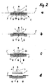
- FIGS. 2a to 2d a slightly modified stripping process is shown. This corresponds to the FIG. 2a partly according to the initial situation FIG. 1a , However, the film 2 is stretched flat over the recesses 7, so that the detachment process does not start at this point.
- To initiate the detachment process is a further step according to FIG. 2b interposed.
- the surface portions 8a, 8b are advanced simultaneously with the holding tool 4 by a small distance in the direction of arrow a, so that the chip 1 to be detached first projects beyond the support plane 11.
- the detachment process in the edge region of the chip 1 is started in a gentle manner. Subsequently, the holding tool 4 is again lowered synchronously with the surface portions 8a, 8b until the film 2 rests again on the support 6. The surface portions 8a, 8b set their movement according Figure 2c in the direction of arrow b, whereupon the rest of the detachment process as described FIG. 1 happening.
- the chip 1 is first touched by means of the holding tool 4, before the surface sections Move 8a and 8b up or down.
- the chip between the holding surface of the holding tool and the surface portions 8a, 8b and the support member 6 is detected by clamping, before any tensile or bending forces act on the film 2.
- this clamping bracket is retained.
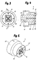
- a release tool 5 is shown, as it can be used for the previously described method.
- the tool consists of a pot-like housing 23 with a hollow cylindrical mounting sleeve 12 and with a support surface 13 on which the film comes to lie in the surrounding area of the chip to be detached.
- the entire inside of the mounting collar can be connected to a vacuum source.
- a negative pressure of 200 mbar absolute can be achieved with respect to the atmospheric pressure.
- On the circular support surface 13 a total of four suction holes 14 are arranged at a uniform angular pitch, via which the wafer film is fixed.
- an approximately square reduction 21 is arranged on the support surface 13.
- an approximately square reduction 21 is arranged within this lowering four approximately triangular ram openings 17 are provided in cloverleaf-like arrangement. Between these ram openings a support strip cross 16 runs and at the intersection of a support pyramid 15 is arranged. Supporting pyramid and support strip cross together form the support element 6, which extends in the support plane 11.
- an approximately cylindrical control element 10 is held axially movable.
- this control four individual tappets 18 are arranged, the configuration of which in the support plane 11 corresponds to the configuration of the tappet openings 17.
- the plungers 18 each have a surface section 8 at their ends and they penetrate the plunger openings 17 with play, so that the vacuum can also act on the wafer foil lying over the recess 21 along their side walls.
- a suction bore 19 can also be arranged in the center of the control element 10.
- the footprint of the chip to be replaced is slightly larger than that of the integrally formed plunger assembly.
- the support is made over the diagonal of the chip and in the center.
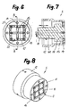
- the fastening collar 12 is substantially similar to the previous embodiment.
- the suction holes 14 in the support surface 13 are arranged identically.
- the configuration of the support surface itself and of the control element 10 is different.
- a square countersink 21 is provided.
- the support element 6 is formed exclusively by supporting pyramids 15, which are each arranged in the corner, in the middle of each side edge and in the center of a matrix.
- a total of four also approximately square plunger openings 17 are arranged in the bottom of the reduction 21. In the edge area can additional holes 22 for better distribution be provided of the negative pressure.
- control surface or the individual surface sections can be heated by means of a heating device 40, which is indicated here as an electric heating cartridge.
- the control element 10 also has four plungers 18 whose configuration corresponds approximately to that of the plunger openings.
- the wafer film is supported in the area of the glued chip exclusively punctiform.
- the function of the removal tool is the same as in the embodiment described above.
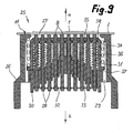
- FIG. 9 shows a modified embodiment of a removal tool 25.
- This has a housing 26 in which possibly a plurality of individual tappets 28 are mounted axially displaceably in a matrix manner.
- the storage of the individual plunger takes place both in a control slide 30 and in a feed element 34.
- the feed element is similar to the housing 26 pot-shaped and has an end face 35 which is slightly recessed below a housing opening 27. In the end face 35 openings are arranged through which the individual plunger 28 penetrate.
- the advancing element 34 is biased against a support 37 on the housing 26 under the action of a helical compression spring 36.
- the spool 30 is lowered even further in the direction of arrow b.
- the spool 30 has a gradation 33 with different levels, wherein in each case two or more individual tappets can be arranged at the same gradation level.
- the individual rams have at the upper end each have a stop 38, which limits the plunger movement upwards.
- the individual tappets are each provided with a driver element 32, wherein in the illustrated neutral starting position all driver elements lie on the same plane.
- the individual tappets are each biased by a helical compression spring 31.
- the vacuum required for the detachment process can act on the wafer film 2 via vacuum channels 29. Additional channels, for example in the individual tappets 28 would be conceivable.
- control surface portions 8 of the individual rams are all in the support plane 11.
- the peculiarity of this embodiment is that the surface portions 8 simultaneously assume the function of a support. This means that in the support plane 11 no relative to the surface portions 8 rigid support is present.
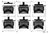
- FIG. 10 is in the individual representations a) to k) a detachment sequence using the removal tool 25 according to FIG. 9 shown.
- a) shows the neutral starting position after placing the wafer film over the removal tool and before the holding tool 4 detects the chip 1.
- the holding tool grasps the chip and the underside of the wafer foil 2 is placed under vacuum.
- the spool 30 is advanced, with the surface portions 8 lifting simultaneously with the holding tool 4.
- the wafer foil 2 is sucked slightly below the support plane 11. Along the outer edges of the chip 1 already begins the removal process.
- control slide 30 is reset again, so that the chip 1 returns to the starting position. All individual rams now have the function of a support for the wafer film. This remains but along the edges in detached position.
- the spool is retracted further, taking the two outermost rams with them and lowering them.
- the wafer foil follows in a guided motion and detaches from the underside of the chip.
- g) and h) follow further withdrawal sequences of the plunger from outside to inside, until at last only the two innermost plunger serve as a support.
- a component (1) bonded to a flexible film (2) in particular a semiconductor chip bonded to a wafer film
- a holding tool (4) for detecting the component on its surface (3) facing away from the film and for lifting it off Film
- at least one control element (10) is movably mounted with a control surface such that the control surface is plane-parallel displaceable from the support plane (11), characterized in that the control surface is at least one plane Surface portion (8) has arranged next to the at least one support element.
- control surface (10) has a plurality of spaced-apart surface sections (8) and that at least between two surface sections (8a, 8b) a support element (6) is arranged.
- the support element (6) has punctiform and / or linear supports for the film.
- the support element comprises a plurality of supporting pyramids or support cone, the matrix-like around the surface portion or the surface sections are arranged.
- control surface can be heated by means of a heating device (40).
Landscapes
- Container, Conveyance, Adherence, Positioning, Of Wafer (AREA)
- Folding Of Thin Sheet-Like Materials, Special Discharging Devices, And Others (AREA)
Applications Claiming Priority (2)
| Application Number | Priority Date | Filing Date | Title |
|---|---|---|---|
| CH00869/04A CH697213A5 (de) | 2004-05-19 | 2004-05-19 | Verfahren und Vorrichtung zum Ablösen eines auf eine flexible Folie geklebten Bauteils. |
| EP04804931A EP1754249A1 (fr) | 2004-05-19 | 2004-12-17 | Procede et dispositif pour enlever un composant colle sur un film souple |
Related Parent Applications (1)
| Application Number | Title | Priority Date | Filing Date |
|---|---|---|---|
| EP04804931.6 Division | 2004-12-17 |
Publications (2)
| Publication Number | Publication Date |
|---|---|
| EP2306496A2 true EP2306496A2 (fr) | 2011-04-06 |
| EP2306496A3 EP2306496A3 (fr) | 2012-10-10 |
Family
ID=34959940
Family Applications (2)
| Application Number | Title | Priority Date | Filing Date |
|---|---|---|---|
| EP10186245A Withdrawn EP2306496A3 (fr) | 2004-05-19 | 2004-12-17 | Procédé et dispositif pour enlever un composant collé sur un film souple |
| EP04804931A Withdrawn EP1754249A1 (fr) | 2004-05-19 | 2004-12-17 | Procede et dispositif pour enlever un composant colle sur un film souple |
Family Applications After (1)
| Application Number | Title | Priority Date | Filing Date |
|---|---|---|---|
| EP04804931A Withdrawn EP1754249A1 (fr) | 2004-05-19 | 2004-12-17 | Procede et dispositif pour enlever un composant colle sur un film souple |
Country Status (6)
| Country | Link |
|---|---|
| US (1) | US7981246B2 (fr) |
| EP (2) | EP2306496A3 (fr) |
| KR (1) | KR101097500B1 (fr) |
| CN (1) | CN101019205B (fr) |
| CH (1) | CH697213A5 (fr) |
| WO (1) | WO2005117072A1 (fr) |
Cited By (1)
| Publication number | Priority date | Publication date | Assignee | Title |
|---|---|---|---|---|
| WO2013171869A1 (fr) * | 2012-05-17 | 2013-11-21 | 富士機械製造株式会社 | Appareil de décollement de puce |
Families Citing this family (22)
| Publication number | Priority date | Publication date | Assignee | Title |
|---|---|---|---|---|
| US8221583B2 (en) * | 2007-01-20 | 2012-07-17 | Stats Chippac Ltd. | System for peeling semiconductor chips from tape |
| CH699851A1 (de) * | 2008-11-05 | 2010-05-14 | Esec Ag | Chip-Auswerfer und Verfahren zum Ablösen und Entnehmen eines Halbleiterchips von einer Folie. |
| MY150953A (en) | 2008-11-05 | 2014-03-31 | Esec Ag | Die-ejector |
| EP2359398B1 (fr) * | 2008-11-12 | 2017-05-10 | Besi Switzerland AG | Procédé pour détacher et prélever une puce de semi-conducteur sur un film |
| KR101026040B1 (ko) | 2008-11-13 | 2011-03-30 | 삼성전기주식회사 | 박막소자 제조방법 |
| KR101046064B1 (ko) | 2008-12-11 | 2011-07-01 | 삼성전기주식회사 | 박막소자 제조방법 |
| IT1393913B1 (it) * | 2009-05-05 | 2012-05-17 | Rent Srl | Gruppo e procedimento di alimentazione di bobine di materiale in foglio, in particolare ma non esclusivamente film plastico stampato con riferimenti di posizione per confezionatrici automatiche |
| EP2284863B1 (fr) | 2009-08-11 | 2012-04-04 | Kulicke & Soffa Die Bonding GmbH | Procédé et appareil d'inspection d'une puce avant la liaison |
| JP5107408B2 (ja) * | 2010-08-31 | 2012-12-26 | 東京エレクトロン株式会社 | ピックアップ方法及びピックアップ装置 |
| DE102011087388A1 (de) * | 2011-02-17 | 2012-08-23 | Semikron Elektronik Gmbh & Co. Kg Ip-Department | Vorrichtung und Verfahren zur Abnahme mindestens eines chipförmigen Halbleiterbauelements von einer Folie |
| CH706280B1 (de) * | 2012-03-30 | 2016-03-15 | Esec Ag | Verfahren zum Ablösen eines Halbleiterchips von einer Folie. |
| KR20140107982A (ko) * | 2013-02-28 | 2014-09-05 | 삼성전자주식회사 | 다이 이젝터 및 다이 분리 방법 |
| US9111984B2 (en) * | 2013-10-28 | 2015-08-18 | Freescale Semiconductor Inc. | Devices and methods of operation for separating semiconductor die from adhesive tape |
| CN103659813A (zh) * | 2013-12-25 | 2014-03-26 | 大连佳峰电子有限公司 | 一种用于半导体晶片吸取的机构运动控制方法 |
| JP2017005222A (ja) * | 2015-06-16 | 2017-01-05 | パイオニア株式会社 | ピックアップ装置 |
| EP3234992B1 (fr) * | 2016-01-29 | 2018-09-26 | JENOPTIK Optical Systems GmbH | Méthode et appareil pour détacher une micro-puce d'une plaquette et placement de la micro-puce sur un substrat |
| TWI567011B (zh) * | 2016-06-15 | 2017-01-21 | 萬潤科技股份有限公司 | Method and device for conveying the components of the bonding process |
| CN107160822B (zh) * | 2017-04-26 | 2018-11-27 | 湖州蓝澳无纬布有限公司 | 一种节能型无纬布生产前期加工处理设备 |
| JP6519761B2 (ja) * | 2017-08-25 | 2019-05-29 | 上野精機株式会社 | 電子部品受渡し装置 |
| CH715447B1 (de) * | 2018-10-15 | 2022-01-14 | Besi Switzerland Ag | Chip-Auswerfer. |
| US12444625B2 (en) * | 2021-12-08 | 2025-10-14 | Samsung Electronics Co., Ltd. | Chip peeling apparatus and chip peeling method using the same |
| CN114188264B (zh) * | 2022-02-15 | 2022-05-03 | 合肥矽迈微电子科技有限公司 | 一种芯片剥离机构、剥离机及剥离方法 |
Citations (7)
| Publication number | Priority date | Publication date | Assignee | Title |
|---|---|---|---|---|
| JPS63228638A (ja) | 1987-03-17 | 1988-09-22 | Sony Corp | チツプ取出し装置 |
| US4778326A (en) | 1983-05-24 | 1988-10-18 | Vichem Corporation | Method and means for handling semiconductor and similar electronic devices |
| JPH0376139A (ja) | 1989-08-18 | 1991-04-02 | Nec Corp | 半導体素子突上げ方法 |
| US6202292B1 (en) | 1998-08-26 | 2001-03-20 | Micron Technology, Inc. | Apparatus for removing carrier film from a semiconductor die |
| JP2001196443A (ja) | 2000-01-14 | 2001-07-19 | Sharp Corp | 半導体チップのピックアップ装置およびピックアップ方法 |
| US20030075271A1 (en) | 2001-10-23 | 2003-04-24 | Fujitsu Limited | Method and device of peeling semiconductor device using annular contact members |
| US6561743B1 (en) | 1999-11-09 | 2003-05-13 | Nec Machinery Corporation | Pellet picking method and pellet picking apparatus |
Family Cites Families (6)
| Publication number | Priority date | Publication date | Assignee | Title |
|---|---|---|---|---|
| US4556362A (en) * | 1983-12-21 | 1985-12-03 | At&T Technologies, Inc. | Methods of and apparatus for handling semiconductor devices |
| JP3076139B2 (ja) | 1992-03-31 | 2000-08-14 | 株式会社名機製作所 | ディスクの射出成形装置 |
| US6352073B1 (en) * | 1998-11-12 | 2002-03-05 | Kabushiki Kaisha Toshiba | Semiconductor manufacturing equipment |
| JP2000353710A (ja) * | 1999-06-14 | 2000-12-19 | Toshiba Corp | ペレットピックアップ装置および半導体装置の製造方法 |
| US7306695B2 (en) * | 2003-04-10 | 2007-12-11 | Matsushita Electric Industrial Co., Ltd. | Apparatus and method for picking up semiconductor chip |
| US7757742B2 (en) * | 2007-07-31 | 2010-07-20 | Asm Assembly Automation Ltd | Vibration-induced die detachment system |
-
2004
- 2004-05-19 CH CH00869/04A patent/CH697213A5/de not_active IP Right Cessation
- 2004-12-17 EP EP10186245A patent/EP2306496A3/fr not_active Withdrawn
- 2004-12-17 CN CN2004800430659A patent/CN101019205B/zh not_active Expired - Lifetime
- 2004-12-17 WO PCT/EP2004/053593 patent/WO2005117072A1/fr not_active Ceased
- 2004-12-17 KR KR1020067025586A patent/KR101097500B1/ko not_active Expired - Fee Related
- 2004-12-17 US US11/596,645 patent/US7981246B2/en active Active
- 2004-12-17 EP EP04804931A patent/EP1754249A1/fr not_active Withdrawn
Patent Citations (7)
| Publication number | Priority date | Publication date | Assignee | Title |
|---|---|---|---|---|
| US4778326A (en) | 1983-05-24 | 1988-10-18 | Vichem Corporation | Method and means for handling semiconductor and similar electronic devices |
| JPS63228638A (ja) | 1987-03-17 | 1988-09-22 | Sony Corp | チツプ取出し装置 |
| JPH0376139A (ja) | 1989-08-18 | 1991-04-02 | Nec Corp | 半導体素子突上げ方法 |
| US6202292B1 (en) | 1998-08-26 | 2001-03-20 | Micron Technology, Inc. | Apparatus for removing carrier film from a semiconductor die |
| US6561743B1 (en) | 1999-11-09 | 2003-05-13 | Nec Machinery Corporation | Pellet picking method and pellet picking apparatus |
| JP2001196443A (ja) | 2000-01-14 | 2001-07-19 | Sharp Corp | 半導体チップのピックアップ装置およびピックアップ方法 |
| US20030075271A1 (en) | 2001-10-23 | 2003-04-24 | Fujitsu Limited | Method and device of peeling semiconductor device using annular contact members |
Cited By (1)
| Publication number | Priority date | Publication date | Assignee | Title |
|---|---|---|---|---|
| WO2013171869A1 (fr) * | 2012-05-17 | 2013-11-21 | 富士機械製造株式会社 | Appareil de décollement de puce |
Also Published As
| Publication number | Publication date |
|---|---|
| EP2306496A3 (fr) | 2012-10-10 |
| HK1111263A1 (en) | 2008-08-01 |
| WO2005117072A1 (fr) | 2005-12-08 |
| KR20070085112A (ko) | 2007-08-27 |
| US20070277929A1 (en) | 2007-12-06 |
| US7981246B2 (en) | 2011-07-19 |
| CN101019205B (zh) | 2010-06-16 |
| KR101097500B1 (ko) | 2011-12-22 |
| EP1754249A1 (fr) | 2007-02-21 |
| CN101019205A (zh) | 2007-08-15 |
| CH697213A5 (de) | 2008-06-25 |
Similar Documents
| Publication | Publication Date | Title |
|---|---|---|
| EP2306496A2 (fr) | Procédé et dispositif pour enlever un composant collé sur un film souple | |
| DE102013103100B4 (de) | Verfahren zum Ablösen eines Halbleiterchips von einer Folie | |
| DE2944810C2 (de) | Montagekopf zum Montieren von elektronischen Bauteilen | |
| DE102011017218B4 (de) | Vorrichtung und Verfahren zum Übertragen elektronischer Bauteile von einem ersten Träger zu einem zweiten Träger | |
| DE102020209954B4 (de) | Schutzelementausbildungsverfahren und schutzelementausbildungsvorrichtung | |
| AT506622B1 (de) | Vorrichtung und verfahren zum aufbringen und/oder ablösen eines wafers auf einen/von einem träger | |
| DE19520053B4 (de) | Bestückungsvorrichtung für Halbleiterelemente | |
| EP2795669B1 (fr) | Support de substrat flexible, dispositif et procédé permettant de détacher un premier substrat | |
| EP1587138B1 (fr) | Dispositif pour la montage de de puces semiconductrices et procédé de séparer de puces semiconductries d'une feuille | |
| EP2184765A1 (fr) | Ejecteur de puce | |
| DE69620854T2 (de) | Vorrichtung zum schrittweise Zuführen sowie Lochen von blattförmigen Materialien | |
| DE10227823B4 (de) | Verfahren und Vorrichtung zum Herstellen eines LCD | |
| EP2359398B1 (fr) | Procédé pour détacher et prélever une puce de semi-conducteur sur un film | |
| EP2390904A2 (fr) | Procédé d'interconnexion de pression à basse température de deux partenaires de liaison et agencement ainsi fabriqué | |
| DE69700286T2 (de) | Verfahren und Vorrichtung zum Abziehen von Chips | |
| DE102016217003A1 (de) | Variabler Maschinentisch | |
| EP2490253B1 (fr) | Dispositif et procédé destinés à extraire au moins un composant semi-conducteur sous forme de puce à partir d'une feuille | |
| EP3443587B1 (fr) | Appareil, système et méthode pour aligner des composants électroniques | |
| EP3362201B1 (fr) | Procédé de fonctionnement d'une presseur plieuse et presse plieuse | |
| AT527300B1 (de) | Vorrichtung zum verbinden eines bauelements mit einem substrat | |
| DE102022118873B4 (de) | Verfahren und Vorrichtung zum Entnehmen von Chips von einem Waferfilmframe, Bestücksystem und Computerprogramm | |
| WO2003085702A1 (fr) | Procede de traitement de composants electriques, notamment de puces a semi-conducteur et dispositif pour mettre ledit procede en oeuvre | |
| DE102009035099B4 (de) | Vorrichtung und Verfahren zum Abheben von Bauteilen von einem Träger | |
| EP3886149A1 (fr) | Dispositif et procédé de liaison de substrats | |
| EP4186107A1 (fr) | Équipement d'une unité de transport lors de la fabrication de panneaux solaires |
Legal Events
| Date | Code | Title | Description |
|---|---|---|---|
| PUAI | Public reference made under article 153(3) epc to a published international application that has entered the european phase |
Free format text: ORIGINAL CODE: 0009012 |
|
| AC | Divisional application: reference to earlier application |
Ref document number: 1754249 Country of ref document: EP Kind code of ref document: P |
|
| AK | Designated contracting states |
Kind code of ref document: A2 Designated state(s): AT BE BG CH CY CZ DE DK EE ES FI FR GB GR HU IE IS IT LI LT LU MC NL PL PT RO SE SI SK TR |
|
| PUAL | Search report despatched |
Free format text: ORIGINAL CODE: 0009013 |
|
| AK | Designated contracting states |
Kind code of ref document: A3 Designated state(s): AT BE BG CH CY CZ DE DK EE ES FI FR GB GR HU IE IS IT LI LT LU MC NL PL PT RO SE SI SK TR |
|
| RIC1 | Information provided on ipc code assigned before grant |
Ipc: H01L 21/00 20060101AFI20120903BHEP |
|
| STAA | Information on the status of an ep patent application or granted ep patent |
Free format text: STATUS: THE APPLICATION IS DEEMED TO BE WITHDRAWN |
|
| 18D | Application deemed to be withdrawn |
Effective date: 20130411 |