EP2306512A2 - Dissipateur de chaleur et modul à haute prestation - Google Patents
Dissipateur de chaleur et modul à haute prestation Download PDFInfo
- Publication number
- EP2306512A2 EP2306512A2 EP11150797A EP11150797A EP2306512A2 EP 2306512 A2 EP2306512 A2 EP 2306512A2 EP 11150797 A EP11150797 A EP 11150797A EP 11150797 A EP11150797 A EP 11150797A EP 2306512 A2 EP2306512 A2 EP 2306512A2
- Authority
- EP
- European Patent Office
- Prior art keywords
- projections
- stress relaxation
- heat radiator
- heat
- relaxation member
- Prior art date
- Legal status (The legal status is an assumption and is not a legal conclusion. Google has not performed a legal analysis and makes no representation as to the accuracy of the status listed.)
- Granted
Links
Images


Classifications
-
- H—ELECTRICITY
- H05—ELECTRIC TECHNIQUES NOT OTHERWISE PROVIDED FOR
- H05K—PRINTED CIRCUITS; CASINGS OR CONSTRUCTIONAL DETAILS OF ELECTRIC APPARATUS; MANUFACTURE OF ASSEMBLAGES OF ELECTRICAL COMPONENTS
- H05K3/00—Apparatus or processes for manufacturing printed circuits
- H05K3/0058—Laminating printed circuit boards onto other substrates, e.g. metallic substrates
- H05K3/0061—Laminating printed circuit boards onto other substrates, e.g. metallic substrates onto a metallic substrate, e.g. a heat sink
-
- H—ELECTRICITY
- H10—SEMICONDUCTOR DEVICES; ELECTRIC SOLID-STATE DEVICES NOT OTHERWISE PROVIDED FOR
- H10W—GENERIC PACKAGES, INTERCONNECTIONS, CONNECTORS OR OTHER CONSTRUCTIONAL DETAILS OF DEVICES COVERED BY CLASS H10
- H10W40/00—Arrangements for thermal protection or thermal control
- H10W40/10—Arrangements for heating
-
- H—ELECTRICITY
- H05—ELECTRIC TECHNIQUES NOT OTHERWISE PROVIDED FOR
- H05K—PRINTED CIRCUITS; CASINGS OR CONSTRUCTIONAL DETAILS OF ELECTRIC APPARATUS; MANUFACTURE OF ASSEMBLAGES OF ELECTRICAL COMPONENTS
- H05K3/00—Apparatus or processes for manufacturing printed circuits
- H05K3/30—Assembling printed circuits with electric components, e.g. with resistors
- H05K3/32—Assembling printed circuits with electric components, e.g. with resistors electrically connecting electric components or wires to printed circuits
- H05K3/34—Assembling printed circuits with electric components, e.g. with resistors electrically connecting electric components or wires to printed circuits by soldering
- H05K3/341—Surface mounted components
-
- H—ELECTRICITY
- H10—SEMICONDUCTOR DEVICES; ELECTRIC SOLID-STATE DEVICES NOT OTHERWISE PROVIDED FOR
- H10W—GENERIC PACKAGES, INTERCONNECTIONS, CONNECTORS OR OTHER CONSTRUCTIONAL DETAILS OF DEVICES COVERED BY CLASS H10
- H10W40/00—Arrangements for thermal protection or thermal control
- H10W40/20—Arrangements for cooling
- H10W40/22—Arrangements for cooling characterised by their shape, e.g. having conical or cylindrical projections
-
- H—ELECTRICITY
- H10—SEMICONDUCTOR DEVICES; ELECTRIC SOLID-STATE DEVICES NOT OTHERWISE PROVIDED FOR
- H10W—GENERIC PACKAGES, INTERCONNECTIONS, CONNECTORS OR OTHER CONSTRUCTIONAL DETAILS OF DEVICES COVERED BY CLASS H10
- H10W40/00—Arrangements for thermal protection or thermal control
- H10W40/20—Arrangements for cooling
- H10W40/22—Arrangements for cooling characterised by their shape, e.g. having conical or cylindrical projections
- H10W40/226—Arrangements for cooling characterised by their shape, e.g. having conical or cylindrical projections characterised by projecting parts, e.g. fins to increase surface area
- H10W40/228—Arrangements for cooling characterised by their shape, e.g. having conical or cylindrical projections characterised by projecting parts, e.g. fins to increase surface area the projecting parts being wire-shaped or pin-shaped
-
- H—ELECTRICITY
- H10—SEMICONDUCTOR DEVICES; ELECTRIC SOLID-STATE DEVICES NOT OTHERWISE PROVIDED FOR
- H10W—GENERIC PACKAGES, INTERCONNECTIONS, CONNECTORS OR OTHER CONSTRUCTIONAL DETAILS OF DEVICES COVERED BY CLASS H10
- H10W40/00—Arrangements for thermal protection or thermal control
- H10W40/20—Arrangements for cooling
- H10W40/25—Arrangements for cooling characterised by their materials
- H10W40/255—Arrangements for cooling characterised by their materials having a laminate or multilayered structure, e.g. direct bond copper [DBC] ceramic substrates
-
- H—ELECTRICITY
- H05—ELECTRIC TECHNIQUES NOT OTHERWISE PROVIDED FOR
- H05K—PRINTED CIRCUITS; CASINGS OR CONSTRUCTIONAL DETAILS OF ELECTRIC APPARATUS; MANUFACTURE OF ASSEMBLAGES OF ELECTRICAL COMPONENTS
- H05K1/00—Printed circuits
- H05K1/02—Details
- H05K1/03—Use of materials for the substrate
- H05K1/0306—Inorganic insulating substrates, e.g. ceramic, glass
-
- H—ELECTRICITY
- H05—ELECTRIC TECHNIQUES NOT OTHERWISE PROVIDED FOR
- H05K—PRINTED CIRCUITS; CASINGS OR CONSTRUCTIONAL DETAILS OF ELECTRIC APPARATUS; MANUFACTURE OF ASSEMBLAGES OF ELECTRICAL COMPONENTS
- H05K2201/00—Indexing scheme relating to printed circuits covered by H05K1/00
- H05K2201/03—Conductive materials
- H05K2201/0332—Structure of the conductor
- H05K2201/0364—Conductor shape
- H05K2201/0373—Conductors having a fine structure, e.g. providing a plurality of contact points with a structured tool
-
- H—ELECTRICITY
- H05—ELECTRIC TECHNIQUES NOT OTHERWISE PROVIDED FOR
- H05K—PRINTED CIRCUITS; CASINGS OR CONSTRUCTIONAL DETAILS OF ELECTRIC APPARATUS; MANUFACTURE OF ASSEMBLAGES OF ELECTRICAL COMPONENTS
- H05K2201/00—Indexing scheme relating to printed circuits covered by H05K1/00
- H05K2201/10—Details of components or other objects attached to or integrated in a printed circuit board
- H05K2201/10227—Other objects, e.g. metallic pieces
- H05K2201/1028—Thin metal strips as connectors or conductors
-
- H—ELECTRICITY
- H05—ELECTRIC TECHNIQUES NOT OTHERWISE PROVIDED FOR
- H05K—PRINTED CIRCUITS; CASINGS OR CONSTRUCTIONAL DETAILS OF ELECTRIC APPARATUS; MANUFACTURE OF ASSEMBLAGES OF ELECTRICAL COMPONENTS
- H05K2203/00—Indexing scheme relating to apparatus or processes for manufacturing printed circuits covered by H05K3/00
- H05K2203/04—Soldering or other types of metallurgic bonding
- H05K2203/0405—Solder foil, tape or wire
-
- H—ELECTRICITY
- H10—SEMICONDUCTOR DEVICES; ELECTRIC SOLID-STATE DEVICES NOT OTHERWISE PROVIDED FOR
- H10W—GENERIC PACKAGES, INTERCONNECTIONS, CONNECTORS OR OTHER CONSTRUCTIONAL DETAILS OF DEVICES COVERED BY CLASS H10
- H10W40/00—Arrangements for thermal protection or thermal control
- H10W40/40—Arrangements for thermal protection or thermal control involving heat exchange by flowing fluids
- H10W40/47—Arrangements for thermal protection or thermal control involving heat exchange by flowing fluids by flowing liquids, e.g. forced water cooling
-
- Y—GENERAL TAGGING OF NEW TECHNOLOGICAL DEVELOPMENTS; GENERAL TAGGING OF CROSS-SECTIONAL TECHNOLOGIES SPANNING OVER SEVERAL SECTIONS OF THE IPC; TECHNICAL SUBJECTS COVERED BY FORMER USPC CROSS-REFERENCE ART COLLECTIONS [XRACs] AND DIGESTS
- Y02—TECHNOLOGIES OR APPLICATIONS FOR MITIGATION OR ADAPTATION AGAINST CLIMATE CHANGE
- Y02P—CLIMATE CHANGE MITIGATION TECHNOLOGIES IN THE PRODUCTION OR PROCESSING OF GOODS
- Y02P70/00—Climate change mitigation technologies in the production process for final industrial or consumer products
- Y02P70/50—Manufacturing or production processes characterised by the final manufactured product
Definitions
- the present invention relates to a heat radiator, and more particularly to a heat radiator which includes an insulating substrate whose first side serves as a heat-generating-element-mounting side, and a heat sink fixed to a second side of the insulating substrate and which radiates, from the heat sink, heat generated from a heat-generating member, such as a semiconductor device, mounted on the insulating substrate.
- a heat radiator which includes an insulating substrate whose first side serves as a heat-generating-element-mounting side, and a heat sink fixed to a second side of the insulating substrate and which radiates, from the heat sink, heat generated from a heat-generating member, such as a semiconductor device, mounted on the insulating substrate.
- aluminum as used herein and in the appended claims encompasses aluminum alloys in addition to pure aluminum, except for the case where “pure aluminum” is specified.
- the semiconductor device In a power module which uses a semiconductor device, such as an IGBT (Insulated Gate Bipolar Transistor), the semiconductor device must be held at a predetermined temperature or lower by means of efficiently radiating heat generated therefrom.
- a heat radiator is used.
- the heat radiator includes an insulating substrate which is formed of a ceramic, such as aluminum oxide (Al 2 O 3 ) or aluminum nitride (AlN), and whose first side serves as a heat-generating-element-mounting side, and a heat sink which is formed of a high-thermal-conduction metal, such as aluminum or copper (including copper alloys; hereinafter, the same is applied), and is soldered to a second side of the insulating substrate.
- a semiconductor device is soldered to the heat-generating-element-mounting side of the insulating substrate of the heat radiator, thereby forming the power module.
- a power module used in, for example, a hybrid car must maintain the heat radiation performance of a heat radiator over a long term.
- the above-mentioned conventional heat radiator involves the following problem. Under some working conditions, thermal stress arises from a difference in coefficient of linear thermal expansion between the insulating substrate and the heat sink and causes cracking in the insulating substrate, cracking in a solder layer which bonds the insulating substrate and the heat sink together, or warpage of a bond surface of the heat sink bonded to the insulating substrate. Such cracking or warpage impairs heat radiation performance.
- a proposed heat radiator in which the above problem is solved includes an insulating substrate whose first side serves as a heat-generating-element-mounting side, a heat radiation member which is soldered to a second side of the insulating substrate, and a heat sink which is screwed on the heat radiation member.
- the heat radiation member includes a pair of platelike heat-radiation-member bodies formed of a high-thermal-conduction material, such as aluminum or copper, and a low-thermal-expansion material, such as an Invar alloy, intervening between the platelike heat-radiation-member bodies. (Refer to Patent Document 1).
- Patent Document 1 Japanese Patent Application Laid-Open (kokai) No. 2004-153075
- An object of the present invention is to solve the above problem and to provide a heat radiator whose material cost is low and which exhibits excellent heat radiation performance.
- the present invention comprises the following modes.
- the stress relaxation member formed of a high-thermal-conduction material intervenes between the insulating substrate and the heat sink and comprises a plate-like body and a plurality of projections formed at intervals on at least one side of the plate-like body, and the stress relaxation member is metal-bonded to the insulating substrate and to the heat sink.
- excellent thermal conductivity is established between the insulating substrate and the heat sink, thereby improving heat radiation performance for radiating heat generated by a semiconductor device mounted on the heat-generating-element-mounting side of the insulating substrate.
- the projections of the stress relaxation member are deformed, thereby relaxing the thermal stress and thus preventing cracking in the insulating substrate, cracking in a bond zone between the insulating substrate and the stress relaxation member, and warpage of the surface of the heat sink located on a side toward the insulating substrate. Accordingly, heat radiation performance is maintained over a long term. Also, since the stress relaxation member comprises the plate-like body and the plurality of projections formed at intervals on at least one side of the plate-like body, cost of the stress relaxation member becomes relatively low, thereby lowering material cost for the heat radiator.
- the plurality of projections are formed on only one side of the plate-like body of the stress relaxation member, and either a side of the plate-like body of the stress relaxation member on which the projections are not formed or end faces of the projections are metal-bonded to the insulating substrate, whereas the side of the plate-like body of the stress relaxation member on which the projections are not formed or the end faces of the projections, whichever are not metal-bonded to the insulating substrate, is metal-bonded to the heat sink.
- excellent thermal conductivity is established between the insulating substrate and the heat sink, thereby improving heat radiation performance for radiating heat generated by a semiconductor device mounted on the heat-generating-element-mounting side of the insulating substrate.
- the projections of the stress relaxation member are deformed, thereby relaxing the thermal stress and thus preventing cracking in the insulating substrate, cracking in a bond zone between the insulating substrate and the stress relaxation member, and warpage of the surface of the heat sink located on a side toward the insulating substrate. Accordingly, heat radiation performance is maintained over a long term. Also, since the stress relaxation member comprises the plate-like body and the plurality of projections formed on only one side of the plate-like body, cost of the stress relaxation member becomes relatively low, thereby lowering material cost for the heat radiator.
- the thermal-conduction plate increases the area of heat transfer between the insulating substrate and heat sink, thermal conductivity between the insulating substrate and the heat sink is further enhanced, thereby improving heat radiation performance for radiating heat generated by a semiconductor device mounted on the heat-generating-element-mounting side of the insulating substrate. Furthermore, even when thermal stress arises in the heat radiator from a difference in coefficient of linear thermal expansion between the insulating substrate and the heat sink, by virtue of the through-holes, the thermal-conduction plate is deformed, thereby relaxing the thermal stress.
- the heat radiator of par. 4 since employment of the two stress relaxation members increases the area of heat transfer between the insulating substrate and heat sink, thermal conductivity between the insulating substrate and the heat sink is further enhanced, thereby improving heat radiation performance for radiating heat generated by a semiconductor device mounted on the heat-generating-element-mounting side of the insulating substrate.
- the projections of the two stress relaxation members are deformed, thereby relaxing the thermal stress and thus preventing cracking in the insulating substrate, cracking in a bond zone between the insulating substrate and the stress relaxation member, and warpage of the surface of the heat sink located on a side toward the insulating substrate.
- high-thermal-conduction grease or a thermal-conduction resin which fills the gaps between the projections of the stress relaxation member further enhances thermal conductivity between the insulating substrate and the heat sink, thereby improving heat radiation performance for radiating heat generated by a semiconductor device mounted on the heat-generating-element-mounting side of the insulating substrate.
- the stress relaxation member is brazed to the insulating substrate and to the heat sink.
- bonding of the stress relaxation member and the insulating substrate and bonding of the stress relaxation member and the heat sink can be performed simultaneously, thereby improving workability in fabrication of the heat radiator.
- the heat radiator described in Patent Document 1 after the insulating substrate and the heat radiation member are soldered together, the heat radiation member and the heat sink must be screwed together; therefore, workability in fabrication of the heat radiator is poor.
- FIGS. 1 , 3 , and 5 will be referred to as "upper,” “lower,” “left,” and “right,” respectively.
- like features or parts are denoted by like reference numerals, and repeated description thereof is omitted.
- FIGS. 1 and 2 The present embodiment is shown in FIGS. 1 and 2 .
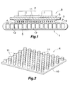
- FIG. 1 shows a portion of a power module which uses a heat radiator of Embodiment 1.
- FIG. 2 shows a stress relaxation member of the heat radiator of Embodiment 1.
- the power module includes a heat radiator 1 and a semiconductor device 2; for example, an IGBT, mounted on the heat radiator 1.
- a semiconductor device 2 for example, an IGBT
- the heat radiator 1 includes an insulating substrate 3 whose upper surface serves as a heat-generating-element-mounting side; a stress relaxation member 4 bonded to the lower surface of the insulating substrate 3; and a heat sink 5 bonded to the lower surface of the stress relaxation member 4.
- the insulating substrate 3 may be formed of any insulating material, so long as it satisfies requirements for insulating characteristics, thermal conductivity, and mechanical strength. For example, when a ceramic is used to form the insulating substrate 3, aluminum oxide or aluminum nitride is used.
- a circuit layer 6 is formed on the upper surface; i.e., the heat-generating-element-mounting side, of the insulating substrate 3, and the semiconductor device 2 is bonded onto the circuit layer 6. This bonding is performed by, for example, soldering. The solder layer is not shown.
- the circuit layer 6 is formed of a metal having excellent electrical conductivity, such as aluminum or copper.
- the circuit layer 6 is formed of a pure aluminum having high purity, which exhibits high electrical conductivity, high deformability, and excellent solderability in relation to a semiconductor device.
- a metal layer 7 is formed on the lower surface of the insulating substrate 3. The stress relaxation member 4 is brazed to the metal layer 7. The brazing-material layer is not shown.
- the metal layer 7 is formed of a metal having excellent thermal conductivity, such as aluminum or copper.
- the metal layer 7 is formed of a pure aluminum having high purity, which exhibits high thermal conductivity, high deformability, and excellent wettability in relation to a molten brazing material.
- the insulating substrate 3, the circuit layer 6, and the metal layer 7 constitute a power module substrate 8.
- the stress relaxation member 4 is formed of a high-thermal-conduction material; herein, aluminum, by, for example, cold-forging.
- the stress relaxation member 4 includes a plate-like body 10 and a plurality of solid, circular, columnar projections 11 which are formed at intervals in a staggered arrangement on the upper surface of the plate-like body 10. The end faces of the projections 11 are brazed to the metal layer 7, and the lower surface of the plate-like body 10 is brazed to the heat sink 5.
- the stress relaxation member 4 is formed of a pure aluminum having a purity of 99% or higher, desirably 99.5% or higher, which exhibits high thermal conductivity, high deformability induced by a drop in strength caused by brazing heat, and excellent wettability in relation to a molten brazing material.
- the thickness of the plate-like body 10 is 0.5 mm to 3 mm. If the plate-like body 10 is excessively thin, at the time of generation of thermal stress in the heat radiator 1 due to a difference in coefficient of thermal expansion between the insulating substrate 3 and the heat sink 5, the deformation of the stress relaxation member 4 becomes insufficient; consequently, the stress relaxation member 4 may fail to sufficiently exhibit stress relaxation performance. If the plate-like body 10 is excessively thick, thermal conductivity drops; consequently, heat radiation performance may drop.
- each of the projections 11 has a projecting height greater than the diameter of its cross section. More preferably, the projecting height of each projection 11 is in excess of 0.8 mm and not greater than 1.5 mm, and the diameter of the cross section of each projection 11 is 0.8 mm or greater and less than 1.5 mm. If the projecting height of each projection 11 is excessively low, and the diameter of the cross section of each projection 11 is excessively large, at the time of generation of thermal stress in the heat radiator 1 due to a difference in coefficient of thermal expansion between the insulating substrate 3 and the heat sink 5, the deformation of the stress relaxation member 4 becomes insufficient; consequently, the stress relaxation member 4 may fail to sufficiently exhibit stress relaxation performance. If the projecting height of each projection 11 is excessively high, and the diameter of the cross section of each projection 11 is excessively small, thermal conductivity drops; consequently, heat radiation performance may drop.
- each of the projections 11 has a projecting height smaller than the diameter of its cross section. More preferably, the projecting height of each projection 11 is 0.5 mm to 0.8 mm, and the diameter of the cross section of each projection 11 is 1.5 mm to 3 mm. If the projecting height of each projection 11 is excessively low, and the diameter of the cross section of each projection 11 is excessively large, at the time of generation of thermal stress in the heat radiator 1 due to a difference in coefficient of thermal expansion between the insulating substrate 3 and the heat sink 5, the deformation of the stress relaxation member 4 becomes insufficient; consequently, the stress relaxation member 4 may fail to sufficiently exhibit stress relaxation performance. If the projecting height of each projection 11 is excessively high, and the diameter of the cross section of each projection 11 is excessively small, thermal conductivity drops; consequently, heat radiation performance may drop.
- the heat sink 5 assumes a flat, hollow shape in which a plurality of cooling-fluid channels 12 are formed in parallel, and is formed of aluminum, which exhibits excellent thermal conductivity and is light.
- a cooling fluid may be either liquid or gas.
- the stress relaxation member 4 is formed of a bare material of the above-mentioned pure aluminum.
- the power module substrate 8, the stress relaxation member 4, and the heat sink 5 are arranged in layers.
- a sheetlike aluminum brazing-material of, for example, an Al-Si alloy or an Al-Si-Mg alloy intervenes between the stress relaxation member 4 and the metal layer 7 of the power module substrate 8 and between the stress relaxation member 4 and the heat sink 5.
- the thickness of the sheetlike aluminum brazing-material is about 10 ⁇ m to 200 ⁇ m. When the thickness is too small, lack of supply of the brazing material arises, potentially causing defective brazing. When the thickness is too large, excess supply of the brazing material arises, potentially causing generation of voids and a drop in thermal conductivity.
- the power module substrate 8, the stress relaxation member 4, and the heat sink 5 are restrained together by use of an appropriate jig to thereby apply an appropriate load to bond surfaces.
- the resultant assembly is heated to 570°C to 600°C in a vacuum or an inert gas atmosphere.
- brazing of the stress relaxation member 4 and the metal layer 7 of the power module substrate 8 to each other and brazing of the stress relaxation member 4 and the heat sink 5 to each other are performed simultaneously.
- the above-mentioned power module is applied to, for example, a vehicle, such as a hybrid car, which uses an electric motor as a part of a drive source, for controlling power to be supplied to the electric motor, according to running conditions of the vehicle.
- Heat generated from the semiconductor device 2 is conducted to the heat sink 5 via the power module substrate 8 and the stress relaxation member 4 and then radiates into the cooling fluid flowing through the cooling-fluid channels 12.
- the insulating substrate 3 and the heat sink 5 assumes high temperature and thermally expands. Meanwhile, when generation of heat from the semiconductor device 2 stops, the insulating substrate 3 and the heat sink 5 drop in temperature to room temperature and thermally contract. At the time of the above-mentioned thermal expansion and thermal contraction, due to a difference in coefficient of linear thermal expansion between the insulating substrate 3 and the heat sink 5, thermal stress are generated in the heat radiator in the left-right direction in FIG. 1 and in the front-back direction of paper on which FIG. 1 appears.
- the projections 11 of the stress relaxation member 4 deform in such a manner that the diameter of the cross section of each projection 11 expands and contracts, thereby relaxing the thermal stress and thus preventing cracking in the insulating substrate 3, cracking in a bond zone between the insulating substrate 3 and the stress relaxation member 4, and warpage of the upper surface of the heat sink 5. Therefore, heat radiation performance is maintained over a long term.
- each projection 11 of the stress relaxation member 4 each assume the form of a solid, circular column.
- the present invention is not limited thereto.
- the outline of the cross section of each projection 11 may be changed as appropriate, so long as each projection 11 assumes the form of a solid column.
- each projection 11 may be prismatic.
- gaps between the projections 11 are filled with high-thermal-conduction grease or a thermal-conduction resin.
- high-thermal-conduction grease include silicone grease, silver paste, and electrically conductive paste.
- An example thermal-conduction resin is epoxy resin. In this case, thermal conductivity from the power module substrate 8 to the heat sink 5 is improved, whereby heat radiation performance becomes excellent.
- FIGS. 3 and 4 The present embodiment is shown in FIGS. 3 and 4 .
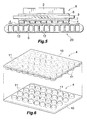
- FIG. 3 shows a portion of a power module which uses a heat radiator of Embodiment 2.
- FIG. 4 shows a stress relaxation member of the heat radiator of Embodiment 2.
- the stress relaxation member 4 similar in constitution to that of Embodiment 1, and a thermal-conduction plate 16 formed of a high-thermal-conduction material; herein, aluminum, and having a plurality of through-holes 17 allowing the respective projections 11 of the stress relaxation member 4 to extend therethrough are disposed between the power module substrate 8 and the heat sink 5 in a heat radiator 15.
- the projections 11 of the stress relaxation member 4 are not formed in a staggered arrangement, but are formed in a grid arrangement.
- the thermal-conduction plate 16 is disposed above the plate-like body 10 of the stress relaxation member 4 in such a manner that the projections 11 extend through the respective through-holes 17, and is brazed to the metal layer 7 of the power module substrate 8.
- a gap is present between the circumferential surfaces of the projections 11 and the corresponding wall surfaces of the through-holes 17.
- a gap is also present between the upper surface of the plate-like body 10 of the stress relaxation member 4 and the lower surface of the thermal-conduction plate 16 (see FIG. 3 ).
- a gap can be formed between the upper surface of the plate-like body 10 of the stress relaxation member 4 and the lower surface of the thermal-conduction plate 16 as follows: brazing of the stress relaxation member 4 and the thermal-conduction plate 16 to the metal layer 7 and brazing of the stress relaxation member 4 to the heat sink 5 are performed in an inverted posture of FIG. 3 .
- a gap is not necessarily required between the upper surface of the plate-like body 10 of the stress relaxation member 4 and the lower surface of the thermal-conduction plate 16.
- the thermal-conduction plate 16 and the plate-like body 10 of the stress relaxation member 4 may be brazed together.
- the thermal-conduction plate 16 is formed of a pure aluminum having a purity of 99% or higher, desirably 99.5% or higher, which exhibits high thermal conductivity, high deformability induced by a drop in strength caused by brazing heat, and excellent wettability in relation to a molten brazing material.
- Brazing of the thermal-conduction plate 16 and the metal layer 7 to each other is performed by use of a sheetlike aluminum brazing-material which is used, in Embodiment 1, for brazing the end faces of the projections 11 to the metal layer.
- this brazing is performed while a sheetlike aluminum brazing-material of, for example, an Al-Si alloy or an Al-Si-Mg alloy having a plurality of through-holes allowing the respective projections 11 to extend therethrough intervenes between the thermal-conduction plate 16 and the plate-like body 10.
- the gaps between the circumferential surfaces of the projections 11 and the corresponding wall surfaces of the through-holes 17 and the gap between the upper surface of the plate-like body 10 of the stress relaxation member 4 and the lower surface of the thermal-conduction plate 16 are filled with high-thermal-conduction grease or a thermal-conduction resin as in the case of Embodiment 1.
- the thermal-conduction plate 16 may be formed of an aluminum brazing sheet which is composed of a core formed of a pure aluminum having a purity of 99% or higher, desirably 99.5% or higher, and aluminum brazing-material layers covering respective opposite sides of the core; and the aluminum brazing-material layers of the aluminum brazing sheet may be used for brazing the thermal-conduction plate 16 and the metal layer 7 together.
- an aluminum brazing-material of the aluminum brazing sheet include an Al-Si alloy and an Al-Si-Mg alloy.
- the thickness of the aluminum brazing-material layer is about 10 ⁇ m to 200 ⁇ m. When the thickness is too small, lack of supply of the brazing material arises, potentially causing defective brazing. When the thickness is too large, excess supply of the brazing material arises, potentially causing generation of voids and a drop in thermal conductivity.
- FIGS. 5 and 6 The present embodiment is shown in FIGS. 5 and 6 .
- FIG. 5 shows a portion of a power module which uses a heat radiator of Embodiment 3.
- FIG. 6 shows a stress relaxation member of the heat radiator of Embodiment 3.
- two stress relaxation members 4 similar in constitution to that of Embodiment 1 are disposed between the power module substrate 8 and the heat sink 5 in a heat radiator 20.
- the upper stress relaxation member 4 is disposed with the projections 11 facing downward, and the lower stress relaxation member 4 is disposed with the projections 11 facing upward.
- the projections 11 of the two stress relaxation members 4 are not formed in a staggered arrangement, but are formed in a grid arrangement.
- the upper surface of the plate-like body 10 of the upper stress relaxation member 4 is brazed to the metal layer 7 of the power module substrate 8, and the lower surface of the plate-like body 10 of the lower stress relaxation member 4 is brazed to the heat sink 5.
- Such brazing is performed by use of a sheetlike aluminum brazing-material.
- the projections 11 of the two stress relaxation members 4 are formed in such a manner as to not interfere with one another between the two stress relaxation members 4.
- the end faces of the projections 11 of the upper stress relaxation member 4 are brazed to the upper surface of the plate-like body 10 of the lower stress relaxation member 4, whereas the end faces of the projections 11 of the lower stress relaxation member 4 are brazed to the lower surface of the plate-like body 10 of the upper stress relaxation member 4.
- Such brazing is performed while a sheetlike aluminum brazing-material of, for example, an Al-Si alloy or an Al-Si-Mg alloy having a plurality of through-holes allowing the respective projections 11 to extend therethrough intervenes between the plate-like bodies 10 and the end faces of the projections 11 of the two stress relaxation members 4.
- a sheetlike aluminum brazing-material of, for example, an Al-Si alloy or an Al-Si-Mg alloy having a plurality of through-holes allowing the respective projections 11 to extend therethrough intervenes between the plate-like bodies 10 and the end faces of the projections 11 of the two stress relaxation members 4.
- the metal layer 7 is formed on the lower surface of the insulating substrate 3 of the power module substrate 8.
- the present invention is not limited thereto.
- the metal layer is not necessarily required.
- the stress relaxation member 4 is brazed directly to the insulating substrate 3.
- the stress relaxation member 4 and the thermal-conduction plate 16 are brazed directly to the insulating substrate.
- FIG. 7 shows a modified stress relaxation member for use in the heat radiators 1, 15, and 20 of Embodiments 1 to 3.
- a stress relaxation member 25 shown in FIG. 7 is formed of a high-thermal-conduction material; herein, aluminum, by, for example, press work.
- the stress relaxation member 25 includes a plate-like body 26 having a plurality of through-holes 27 formed in a staggered arrangement, and hollow, cylindrical projections 28 formed integrally with the plate-like body 26 and standing around the respective through-holes 27.
- the thickness of the plate-like body 26 is 0.5 mm to 3 mm. If the plate-like body 26 is excessively thin, at the time of generation of thermal stress in the heat radiator 1, 15, or 20 due to a difference in coefficient of thermal expansion between the insulating substrate 3 and the heat sink 5, the deformation of the stress relaxation member 25 becomes insufficient; consequently, the stress relaxation member 25 may fail to sufficiently exhibit stress relaxation performance. If the plate-like body 26 is excessively thick, thermal conductivity drops; consequently, heat radiation performance may drop.
- each of the projections 28 has a projecting height greater than the diameter of its cross section. More preferably, the projecting height of each projection 28 is in excess of 0.8 mm and not greater than 1.5 mm, and the diameter of the cross section of each projection 28 is 0.8 mm or greater and less than 1.5 mm.
- each projection 28 If the projecting height of each projection 28 is excessively low, and the diameter of the cross section of each projection 28 is excessively large, at the time of generation of thermal stress in the heat radiator 1, 15, or 20 due to a difference in coefficient of thermal expansion between the insulating substrate 3 and the heat sink 5, the deformation of the stress relaxation member 25 becomes insufficient; consequently, the stress relaxation member 25 may fail to sufficiently exhibit stress relaxation performance. If the projecting height of each projection 28 is excessively high, and the diameter of the cross section of each projection 28 is excessively small, thermal conductivity drops; consequently, heat radiation performance may drop.
- each of the projections 28 has a projecting height smaller than the diameter of its cross section. More preferably, the projecting height of each projection 28 is 0.5 mm to 0.8 mm, and the diameter of the cross section of each projection 28 is 1.5 mm to 3 mm. If the projecting height of each projection 28 is excessively low, and the diameter of the cross section of each projection 28 is excessively large, at the time of generation of thermal stress in the heat radiator 1, 15, or 20 due to a difference in coefficient of thermal expansion between the insulating substrate 3 and the heat sink 5, the deformation of the stress relaxation member 25 becomes insufficient; consequently, the stress relaxation member 25 may fail to sufficiently exhibit stress relaxation performance. If the projecting height of each projection 28 is excessively high, and the diameter of the cross section of each projection 28 is excessively small, thermal conductivity drops; consequently, heat radiation performance may drop.
- the stress relaxation member 25 is formed of a pure aluminum having a purity of 99% or higher, desirably 99.5% or higher.
- the stress relaxation member 25 in addition to filling the gaps with high-thermal-conduction grease or a thermal-conduction resin as mentioned in the description of Embodiments 1 to 3, the interiors of the projections 28 are filled with high-thermal-conduction grease or a thermal-conduction resin.
- the stress relaxation member 25 shown in FIG. 7 may be formed of an aluminum brazing sheet which is composed of a core formed of a pure aluminum having a purity of 99% or higher, desirably 99.5% or higher, and aluminum brazing-material layers covering respective opposite sides of the core; and the aluminum brazing-material layers of the aluminum brazing sheet may be used for brazing the stress relaxation member 25.
- Examples of an aluminum brazing-material of the aluminum brazing sheet include an Al-Si alloy and an Al-Si-Mg alloy.
- the thickness of the aluminum brazing-material layer is about 10 ⁇ m to 200 ⁇ m. When the thickness is too small, lack of supply of the brazing material arises, potentially causing defective brazing. When the thickness is too large, excess supply of the brazing material arises, potentially causing generation of voids and a drop in thermal conductivity.
- FIG. 8 shows a modified stress relaxation member and a modified thermal-conduction plate for use in the heat radiator 15 of Embodiment 2.
- projections 31 formed on the upper surface of the plate-like body 10 of a stress relaxation member 30 each assume the form of a solid prism, and a thermal-conduction plate 32 has a plurality of rectangular through-holes 33 allowing the respective projections 31 to extend therethrough.
Landscapes
- Engineering & Computer Science (AREA)
- Manufacturing & Machinery (AREA)
- Microelectronics & Electronic Packaging (AREA)
- Cooling Or The Like Of Semiconductors Or Solid State Devices (AREA)
Applications Claiming Priority (2)
| Application Number | Priority Date | Filing Date | Title |
|---|---|---|---|
| JP2005198288A JP4617209B2 (ja) | 2005-07-07 | 2005-07-07 | 放熱装置 |
| EP20060767882 EP1901350A4 (fr) | 2005-07-07 | 2006-07-05 | Dispositif dissipateur de chaleur et module de puissance |
Related Parent Applications (2)
| Application Number | Title | Priority Date | Filing Date |
|---|---|---|---|
| EP06767882.1 Division | 2006-07-05 | ||
| EP20060767882 Division EP1901350A4 (fr) | 2005-07-07 | 2006-07-05 | Dispositif dissipateur de chaleur et module de puissance |
Publications (3)
| Publication Number | Publication Date |
|---|---|
| EP2306512A2 true EP2306512A2 (fr) | 2011-04-06 |
| EP2306512A3 EP2306512A3 (fr) | 2012-08-08 |
| EP2306512B1 EP2306512B1 (fr) | 2014-09-03 |
Family
ID=37636996
Family Applications (2)
| Application Number | Title | Priority Date | Filing Date |
|---|---|---|---|
| EP20060767882 Withdrawn EP1901350A4 (fr) | 2005-07-07 | 2006-07-05 | Dispositif dissipateur de chaleur et module de puissance |
| EP11150797.6A Not-in-force EP2306512B1 (fr) | 2005-07-07 | 2006-07-05 | Dissipateur de chaleur et modul à haute prestation |
Family Applications Before (1)
| Application Number | Title | Priority Date | Filing Date |
|---|---|---|---|
| EP20060767882 Withdrawn EP1901350A4 (fr) | 2005-07-07 | 2006-07-05 | Dispositif dissipateur de chaleur et module de puissance |
Country Status (6)
| Country | Link |
|---|---|
| US (1) | US8198539B2 (fr) |
| EP (2) | EP1901350A4 (fr) |
| JP (1) | JP4617209B2 (fr) |
| KR (1) | KR101215695B1 (fr) |
| CN (1) | CN100578768C (fr) |
| WO (1) | WO2007007602A1 (fr) |
Cited By (1)
| Publication number | Priority date | Publication date | Assignee | Title |
|---|---|---|---|---|
| DE102020108808A1 (de) | 2020-03-31 | 2021-09-30 | Audi Aktiengesellschaft | Batteriezellenanordnung und Kraftfahrzeug mit einer Batteriezellenanordnung |
Families Citing this family (87)
| Publication number | Priority date | Publication date | Assignee | Title |
|---|---|---|---|---|
| JP4621531B2 (ja) * | 2005-04-06 | 2011-01-26 | 株式会社豊田自動織機 | 放熱装置 |
| JP5064111B2 (ja) * | 2006-06-28 | 2012-10-31 | 株式会社ティラド | 複合放熱板およびその製造方法並びに、それに用いる熱応力緩和プレート |
| JP2008053693A (ja) * | 2006-07-28 | 2008-03-06 | Sanyo Electric Co Ltd | 半導体モジュール、携帯機器、および半導体モジュールの製造方法 |
| EP1936683A1 (fr) * | 2006-12-22 | 2008-06-25 | ABB Technology AG | Plaque de base pour dissipateur thermique et dispositif électronique avec plaque de base |
| JP4694514B2 (ja) * | 2007-02-08 | 2011-06-08 | トヨタ自動車株式会社 | 半導体素子の冷却構造 |
| JP4697475B2 (ja) * | 2007-05-21 | 2011-06-08 | トヨタ自動車株式会社 | パワーモジュールの冷却器及びパワーモジュール |
| JP5185566B2 (ja) * | 2007-05-22 | 2013-04-17 | 株式会社ティラド | セラミック回路基板構造 |
| JP4867793B2 (ja) * | 2007-05-25 | 2012-02-01 | 株式会社豊田自動織機 | 半導体装置 |
| JP4945319B2 (ja) * | 2007-05-25 | 2012-06-06 | 昭和電工株式会社 | 半導体装置 |
| US7915727B2 (en) | 2007-07-20 | 2011-03-29 | Samsung Electronics Co., Ltd. | Tape for heat dissipating member, chip on film type semiconductor package including heat dissipating member, and electronic apparatus including the same |
| JP2009130060A (ja) * | 2007-11-21 | 2009-06-11 | Toyota Industries Corp | 放熱装置 |
| JP5070014B2 (ja) * | 2007-11-21 | 2012-11-07 | 株式会社豊田自動織機 | 放熱装置 |
| JP5022916B2 (ja) * | 2008-01-08 | 2012-09-12 | 株式会社東芝 | 発熱体搭載可能部品、金属体及び発熱体搭載可能部品の取付構造 |
| JP2009212390A (ja) * | 2008-03-05 | 2009-09-17 | Toshiba Corp | 発熱体搭載部品の取付構造 |
| JP4471023B2 (ja) * | 2008-06-12 | 2010-06-02 | ダイキン工業株式会社 | 空気調和機 |
| US8963323B2 (en) | 2008-06-20 | 2015-02-24 | Alcatel Lucent | Heat-transfer structure |
| US8472193B2 (en) | 2008-07-04 | 2013-06-25 | Kabushiki Kaisha Toyota Jidoshokki | Semiconductor device |
| EP2166569A1 (fr) * | 2008-09-22 | 2010-03-24 | ABB Schweiz AG | Dispositif de refroidissement pour un composant de puissance |
| EP2178117A1 (fr) * | 2008-10-17 | 2010-04-21 | Abb Research Ltd. | Module d'alimentation semi-conducteur doté d'un refroidissement à double face |
| DE102009000514A1 (de) | 2009-01-30 | 2010-08-26 | Robert Bosch Gmbh | Verbundbauteil sowie Verfahren zum Herstellen eines Verbundbauteil |
| JP5120284B2 (ja) | 2009-02-04 | 2013-01-16 | 株式会社豊田自動織機 | 半導体装置 |
| JP5292556B2 (ja) * | 2009-03-17 | 2013-09-18 | 株式会社Welcon | 熱伝導複合材及びその製造方法 |
| JP5481961B2 (ja) * | 2009-06-24 | 2014-04-23 | トヨタ自動車株式会社 | 半導体装置 |
| JP5515947B2 (ja) * | 2010-03-29 | 2014-06-11 | 株式会社豊田自動織機 | 冷却装置 |
| JP5382049B2 (ja) * | 2010-06-30 | 2014-01-08 | 株式会社デンソー | 半導体装置 |
| JP5672305B2 (ja) * | 2010-08-27 | 2015-02-18 | 株式会社村田製作所 | 半導体装置 |
| US8587116B2 (en) | 2010-09-30 | 2013-11-19 | Infineon Technologies Ag | Semiconductor module comprising an insert |
| JP5392272B2 (ja) * | 2011-01-13 | 2014-01-22 | 株式会社豊田自動織機 | 両面基板、半導体装置、半導体装置の製造方法 |
| KR101184508B1 (ko) * | 2011-02-08 | 2012-09-19 | 삼성전기주식회사 | 인쇄회로기판 |
| CN102655126B (zh) * | 2011-03-01 | 2016-08-03 | 三菱综合材料株式会社 | 功率模块用基板及制法、自带散热器的该基板及功率模块 |
| JP5349572B2 (ja) * | 2011-04-18 | 2013-11-20 | 株式会社豊田自動織機 | 放熱装置及び放熱装置の製造方法 |
| KR101255935B1 (ko) * | 2011-07-08 | 2013-04-23 | 삼성전기주식회사 | 전력 모듈 패키지 및 그 제조방법 |
| JP6216964B2 (ja) * | 2011-08-09 | 2017-10-25 | 三菱アルミニウム株式会社 | 冷却器用クラッド材および発熱素子用冷却器 |
| CN102427070A (zh) * | 2011-12-14 | 2012-04-25 | 深圳市威怡电气有限公司 | 功率模块 |
| JP5856838B2 (ja) * | 2011-12-22 | 2016-02-10 | 昭和電工株式会社 | 放熱装置用ろう材箔 |
| JP5831273B2 (ja) * | 2012-02-09 | 2015-12-09 | 三菱電機株式会社 | 半導体装置およびその製造方法 |
| JP2013229579A (ja) * | 2012-03-30 | 2013-11-07 | Mitsubishi Materials Corp | パワーモジュール用基板、ヒートシンク付パワーモジュール用基板及びパワーモジュール |
| JP6189015B2 (ja) * | 2012-04-19 | 2017-08-30 | 昭和電工株式会社 | 放熱装置および放熱装置の製造方法 |
| US8872332B2 (en) * | 2012-04-30 | 2014-10-28 | Infineon Technologies Ag | Power module with directly attached thermally conductive structures |
| JP2014017318A (ja) * | 2012-07-06 | 2014-01-30 | Toyota Industries Corp | 半導体装置 |
| DE102012213573B3 (de) | 2012-08-01 | 2013-09-26 | Infineon Technologies Ag | Halbleitermodulanordnung und verfahren zur herstellung und zum betrieb einer halbleitermodulanordnung |
| CN103002722B (zh) * | 2012-12-18 | 2015-03-25 | 武汉光迅科技股份有限公司 | 一种功率设备的热控制装置 |
| US8872328B2 (en) * | 2012-12-19 | 2014-10-28 | General Electric Company | Integrated power module package |
| JP6064886B2 (ja) * | 2012-12-26 | 2017-01-25 | 株式会社豊田中央研究所 | 熱伝導性応力緩和構造体 |
| KR101755966B1 (ko) * | 2013-02-28 | 2017-07-07 | 미쓰비시덴키 가부시키가이샤 | 방열 구조 및 광 송수신기 |
| US9470720B2 (en) * | 2013-03-08 | 2016-10-18 | Sandisk Technologies Llc | Test system with localized heating and method of manufacture thereof |
| JP6197329B2 (ja) * | 2013-03-28 | 2017-09-20 | 三菱マテリアル株式会社 | パワーモジュール、及び熱インターフェース板の製造方法 |
| JP6197365B2 (ja) * | 2013-05-21 | 2017-09-20 | 三菱マテリアル株式会社 | パワーモジュール、及び熱インターフェース板の製造方法 |
| US9898056B2 (en) | 2013-06-19 | 2018-02-20 | Sandisk Technologies Llc | Electronic assembly with thermal channel and method of manufacture thereof |
| US10013033B2 (en) | 2013-06-19 | 2018-07-03 | Sandisk Technologies Llc | Electronic assembly with thermal channel and method of manufacture thereof |
| JP5999041B2 (ja) * | 2013-07-23 | 2016-09-28 | 株式会社デンソー | 電子装置 |
| CN103413794A (zh) * | 2013-08-16 | 2013-11-27 | 中国科学院深圳先进技术研究院 | 一种半导体功率器件的散热封装结构 |
| EP2854170B1 (fr) | 2013-09-27 | 2022-01-26 | Alcatel Lucent | Structure pour une interface de transfert de chaleur et son procédé de fabrication |
| CN103579131A (zh) * | 2013-11-04 | 2014-02-12 | 株洲南车时代电气股份有限公司 | 用于功率igbt模块封装的无曲度基板 |
| JP6308780B2 (ja) * | 2013-12-27 | 2018-04-11 | 三菱電機株式会社 | パワーモジュール |
| CN105849904B (zh) * | 2013-12-27 | 2018-09-07 | 三菱电机株式会社 | 半导体装置 |
| US9549457B2 (en) | 2014-02-12 | 2017-01-17 | Sandisk Technologies Llc | System and method for redirecting airflow across an electronic assembly |
| US9497889B2 (en) | 2014-02-27 | 2016-11-15 | Sandisk Technologies Llc | Heat dissipation for substrate assemblies |
| US9485851B2 (en) | 2014-03-14 | 2016-11-01 | Sandisk Technologies Llc | Thermal tube assembly structures |
| US9348377B2 (en) | 2014-03-14 | 2016-05-24 | Sandisk Enterprise Ip Llc | Thermal isolation techniques |
| US9519319B2 (en) | 2014-03-14 | 2016-12-13 | Sandisk Technologies Llc | Self-supporting thermal tube structure for electronic assemblies |
| DE102015202300A1 (de) * | 2015-02-10 | 2016-08-11 | Robert Bosch Gmbh | Wärmetransferblech |
| US9559026B2 (en) * | 2015-02-26 | 2017-01-31 | Infineon Technologies Americas Corp. | Semiconductor package having a multi-layered base |
| US10287161B2 (en) * | 2015-07-23 | 2019-05-14 | Analog Devices, Inc. | Stress isolation features for stacked dies |
| DE112016006332B4 (de) * | 2016-01-28 | 2021-02-04 | Mitsubishi Electric Corporation | Leistungsmodul |
| DE102016218522B3 (de) * | 2016-09-27 | 2017-06-22 | Jenoptik Laser Gmbh | Optische oder optoelektronische Baugruppe und Verfahren zur Herstellung dafür |
| US11152280B2 (en) * | 2016-11-24 | 2021-10-19 | Mitsubishi Electric Corporation | Semiconductor device and method for manufacturing the same |
| JP6595531B2 (ja) * | 2017-05-30 | 2019-10-23 | ファナック株式会社 | ヒートシンクアッセンブリ |
| US11127716B2 (en) | 2018-04-12 | 2021-09-21 | Analog Devices International Unlimited Company | Mounting structures for integrated device packages |
| US10490482B1 (en) * | 2018-12-05 | 2019-11-26 | Toyota Motor Engineering & Manufacturing North America, Inc. | Cooling devices including jet cooling with an intermediate mesh and methods for using the same |
| FR3089750B1 (fr) * | 2018-12-11 | 2021-07-16 | Valeo Equip Electr Moteur | Convertisseur de tension et procédé de fabrication d’un convertisseur de tension |
| CN109769341B (zh) * | 2019-01-28 | 2022-01-21 | 晶晨半导体(深圳)有限公司 | 一种用于解决金属散热片的天线效应的方法 |
| TWI743557B (zh) | 2019-09-05 | 2021-10-21 | 朋程科技股份有限公司 | 功率元件封裝結構 |
| CN112490202A (zh) * | 2019-09-12 | 2021-03-12 | 朋程科技股份有限公司 | 功率器件封装结构 |
| US11774190B2 (en) * | 2020-04-14 | 2023-10-03 | International Business Machines Corporation | Pierced thermal interface constructions |
| JP6849137B1 (ja) * | 2020-07-06 | 2021-03-24 | 富士電機株式会社 | 半導体装置 |
| US11664340B2 (en) | 2020-07-13 | 2023-05-30 | Analog Devices, Inc. | Negative fillet for mounting an integrated device die to a carrier |
| JP6841367B1 (ja) * | 2020-07-14 | 2021-03-10 | 富士電機株式会社 | 半導体モジュール、電力変換装置及び半導体モジュールの製造方法 |
| DE102020128453A1 (de) | 2020-10-29 | 2022-05-05 | Erwin Quarder Systemtechnik Gmbh | Kompensationsbauteil |
| DE102021109658B3 (de) | 2021-04-16 | 2022-10-20 | Danfoss Silicon Power Gmbh | Verfahren zur Herstellung eines Halbleiter-Leistungsgeräts und damit hergestelltes Halbleiter-Leistungsgerät sowie ein Werkzeugteil für eine Sinterpresse und Verwendung einer Sinterpresse |
| DE102021109666B3 (de) | 2021-04-16 | 2022-10-20 | Danfoss Silicon Power Gmbh | Elektronisches Gerät und Verfahren zu dessen Herstellung |
| US20240274489A1 (en) * | 2021-06-18 | 2024-08-15 | Mitsubishi Electric Corporation | Power Semiconductor Device, Method for Manufacturing Same, and Power Conversion Device |
| KR102720892B1 (ko) * | 2021-07-27 | 2024-10-23 | 주식회사 아모센스 | 히트싱크 일체형 세라믹 기판 및 그 제조방법 |
| KR20230126876A (ko) * | 2022-02-24 | 2023-08-31 | 주식회사 아모그린텍 | 세라믹 기판 유닛 및 그 제조방법 |
| TWM630490U (zh) * | 2022-05-06 | 2022-08-01 | 藍天電腦股份有限公司 | 散熱模組 |
| DE102022123868A1 (de) * | 2022-08-22 | 2024-02-22 | Elringklinger Ag | Entwärmungsvorrichtung |
| CN121751561A (zh) * | 2024-09-24 | 2026-03-27 | 台达电子工业股份有限公司 | 散热装置及其适用的功率模块 |
Citations (1)
| Publication number | Priority date | Publication date | Assignee | Title |
|---|---|---|---|---|
| JP2004153075A (ja) | 2002-10-31 | 2004-05-27 | Mitsubishi Materials Corp | パワーモジュール用基板及びパワーモジュール |
Family Cites Families (56)
| Publication number | Priority date | Publication date | Assignee | Title |
|---|---|---|---|---|
| US4069498A (en) * | 1976-11-03 | 1978-01-17 | International Business Machines Corporation | Studded heat exchanger for integrated circuit package |
| DE3031912A1 (de) * | 1980-08-23 | 1982-04-01 | Brown, Boveri & Cie Ag, 6800 Mannheim | Anordnung zur potentialunabhaengigen waermeabfuehrung |
| US5631447A (en) * | 1988-02-05 | 1997-05-20 | Raychem Limited | Uses of uniaxially electrically conductive articles |
| JP2655426B2 (ja) * | 1988-10-11 | 1997-09-17 | 日本電気株式会社 | 半導体装置 |
| JP3253063B2 (ja) | 1989-07-20 | 2002-02-04 | キヤノン株式会社 | カラー画像処理装置 |
| JP2675173B2 (ja) * | 1990-03-02 | 1997-11-12 | 株式会社日立製作所 | 電子デバイスの冷却装置 |
| JP2838154B2 (ja) * | 1990-07-11 | 1998-12-16 | 京セラ株式会社 | 放熱体の製造方法 |
| JPH04123441A (ja) * | 1990-09-14 | 1992-04-23 | Hitachi Ltd | 半導体集積回路装置 |
| US5111278A (en) * | 1991-03-27 | 1992-05-05 | Eichelberger Charles W | Three-dimensional multichip module systems |
| US5760333A (en) * | 1992-08-06 | 1998-06-02 | Pfu Limited | Heat-generating element cooling device |
| DE59407670D1 (de) * | 1993-04-16 | 1999-03-04 | Heinze Dyconex Patente | Kern für elektrische Verbindungssubstrate und elektrische Verbindungssubstrate mit Kern, sowie Verfahren zu deren Herstellung |
| US5510650A (en) * | 1994-09-02 | 1996-04-23 | General Motors Corporation | Low mechanical stress, high electrical and thermal conductance semiconductor die mount |
| US5707756A (en) * | 1994-11-29 | 1998-01-13 | Fuji Photo Film Co., Ltd. | Non-aqueous secondary battery |
| US5623160A (en) * | 1995-09-14 | 1997-04-22 | Liberkowski; Janusz B. | Signal-routing or interconnect substrate, structure and apparatus |
| US5981085A (en) * | 1996-03-21 | 1999-11-09 | The Furukawa Electric Co., Inc. | Composite substrate for heat-generating semiconductor device and semiconductor apparatus using the same |
| US5787976A (en) * | 1996-07-01 | 1998-08-04 | Digital Equipment Corporation | Interleaved-fin thermal connector |
| US5737187A (en) * | 1996-08-26 | 1998-04-07 | Compaq Computer Corporation | Apparatus, method and system for thermal management of an unpackaged semiconductor device |
| US5930115A (en) * | 1996-08-26 | 1999-07-27 | Compaq Computer Corp. | Apparatus, method and system for thermal management of a semiconductor device |
| US6058012A (en) * | 1996-08-26 | 2000-05-02 | Compaq Computer Corporation | Apparatus, method and system for thermal management of an electronic system having semiconductor devices |
| WO1998020549A1 (fr) * | 1996-11-08 | 1998-05-14 | W.L. Gore & Associates, Inc. | Utilisation d'une densite de perforation variable de la couche de cuivre pour commander le coefficient de dilatation thermique |
| JPH10189845A (ja) * | 1996-12-25 | 1998-07-21 | Denso Corp | 半導体素子の放熱装置 |
| US5952840A (en) * | 1996-12-31 | 1999-09-14 | Micron Technology, Inc. | Apparatus for testing semiconductor wafers |
| US6245442B1 (en) * | 1997-05-28 | 2001-06-12 | Kabushiki Kaisha Toyota Chuo | Metal matrix composite casting and manufacturing method thereof |
| US6374490B1 (en) * | 1998-08-12 | 2002-04-23 | Nakamura Seisakusho Kabushikigaisha | Method of forming a hollow pole projecting on a plate and a method of manufacturing a heat sink using said method |
| JP2000082887A (ja) * | 1998-09-07 | 2000-03-21 | Sony Corp | ヒートシンク用の伝熱シート |
| US6423596B1 (en) * | 1998-09-29 | 2002-07-23 | Texas Instruments Incorporated | Method for two-sided fabrication of a memory array |
| US6906292B2 (en) * | 1998-10-29 | 2005-06-14 | Applera Corporation | Sample tray heater module |
| JP2000150736A (ja) * | 1998-11-13 | 2000-05-30 | Shinko Electric Ind Co Ltd | 半導体モジュール用放熱板および半導体モジュール |
| US7584780B1 (en) * | 1998-12-09 | 2009-09-08 | Lemont Aircraft Corporation | Active heat sink structure with flow augmenting rings and method for removing heat |
| US6896039B2 (en) * | 1999-05-12 | 2005-05-24 | Thermal Corp. | Integrated circuit heat pipe heat spreader with through mounting holes |
| US6239972B1 (en) * | 1999-12-13 | 2001-05-29 | Honeywell International Inc. | Integrated convection and conduction heat sink for multiple mounting positions |
| JP4386522B2 (ja) * | 2000-01-26 | 2009-12-16 | 株式会社ルネサステクノロジ | 半導体装置の製造方法 |
| US6956757B2 (en) * | 2000-06-22 | 2005-10-18 | Contour Semiconductor, Inc. | Low cost high density rectifier matrix memory |
| ATE425556T1 (de) * | 2001-04-12 | 2009-03-15 | Matsushita Electric Works Ltd | Lichtquellenbauelement mit led und verfahren zu seiner herstellung |
| JP4969738B2 (ja) * | 2001-06-28 | 2012-07-04 | 株式会社東芝 | セラミックス回路基板およびそれを用いた半導体モジュール |
| JP2003051144A (ja) * | 2001-08-03 | 2003-02-21 | Fujitsu Ltd | 磁気ヘッド |
| EP1369931A1 (fr) * | 2002-06-03 | 2003-12-10 | Hitachi, Ltd. | Cellule solaire et son procédé de fabrication et plaque métallique |
| WO2004008142A1 (fr) * | 2002-07-12 | 2004-01-22 | Mitsubishi Chemical Corporation | Puce d'analyse, unite de puce d'analyse, appareil d'analyse, methode d'analyse effectuee avec l'appareil et procede de production de la puce d'analyse |
| JP2004087612A (ja) * | 2002-08-23 | 2004-03-18 | Toyota Industries Corp | 放熱部材及びこの放熱部材を用いた半導体装置 |
| US6994151B2 (en) * | 2002-10-22 | 2006-02-07 | Cooligy, Inc. | Vapor escape microchannel heat exchanger |
| US7836597B2 (en) * | 2002-11-01 | 2010-11-23 | Cooligy Inc. | Method of fabricating high surface to volume ratio structures and their integration in microheat exchangers for liquid cooling system |
| US7000684B2 (en) * | 2002-11-01 | 2006-02-21 | Cooligy, Inc. | Method and apparatus for efficient vertical fluid delivery for cooling a heat producing device |
| WO2004042306A2 (fr) * | 2002-11-01 | 2004-05-21 | Cooligy, Inc. | Procede et appareil d'obtention de l'uniformite thermique et de refroidissement de point chaud dans un dispositif de production de chaleur |
| US7396735B2 (en) * | 2002-12-09 | 2008-07-08 | Kabushiki Kaisha Toyota Chuo Kenkyusyo | Semiconductor element heat dissipating member, semiconductor device using same, and method for manufacturing same |
| JP2004205159A (ja) * | 2002-12-26 | 2004-07-22 | Denso Corp | 熱交換器 |
| US7828620B2 (en) * | 2003-01-09 | 2010-11-09 | Sony Corporation | Method of manufacturing tubular carbon molecule and tubular carbon molecule, method of manufacturing field electron emission device and field electron emission device, and method of manufacturing display unit and display unit |
| JP3934565B2 (ja) * | 2003-02-21 | 2007-06-20 | 富士通株式会社 | 半導体装置 |
| DE10337640A1 (de) * | 2003-08-16 | 2005-03-17 | Semikron Elektronik Gmbh | Leistungshalbleitermodul mit verbessertem thermischen Kontakt |
| JP4123441B2 (ja) | 2003-08-18 | 2008-07-23 | 株式会社デンソー | 車両用突入電流制限型電源スイッチ回路 |
| KR100542188B1 (ko) * | 2003-08-26 | 2006-01-10 | 삼성에스디아이 주식회사 | 플라즈마 디스플레이 장치 |
| JP2006156711A (ja) * | 2004-11-30 | 2006-06-15 | Mitsubishi Electric Corp | パワー半導体モジュールの冷却システム |
| JP4688526B2 (ja) * | 2005-03-03 | 2011-05-25 | Okiセミコンダクタ株式会社 | 半導体装置及びその製造方法 |
| JP4974568B2 (ja) * | 2005-04-06 | 2012-07-11 | エルジー ディスプレイ カンパニー リミテッド | 電界発光表示装置 |
| JP4439441B2 (ja) * | 2005-07-01 | 2010-03-24 | 富士通株式会社 | 熱交換器 |
| US20070077349A1 (en) * | 2005-09-30 | 2007-04-05 | Eastman Kodak Company | Patterning OLED device electrodes and optical material |
| JP5103731B2 (ja) * | 2005-12-12 | 2012-12-19 | 三菱電機株式会社 | モールドパッケージ |
-
2005
- 2005-07-07 JP JP2005198288A patent/JP4617209B2/ja not_active Expired - Fee Related
-
2006
- 2006-07-05 US US11/994,896 patent/US8198539B2/en not_active Expired - Fee Related
- 2006-07-05 WO PCT/JP2006/313376 patent/WO2007007602A1/fr not_active Ceased
- 2006-07-05 CN CN200680024815A patent/CN100578768C/zh not_active Expired - Fee Related
- 2006-07-05 EP EP20060767882 patent/EP1901350A4/fr not_active Withdrawn
- 2006-07-05 EP EP11150797.6A patent/EP2306512B1/fr not_active Not-in-force
-
2008
- 2008-02-05 KR KR1020087003036A patent/KR101215695B1/ko not_active Expired - Fee Related
Patent Citations (1)
| Publication number | Priority date | Publication date | Assignee | Title |
|---|---|---|---|---|
| JP2004153075A (ja) | 2002-10-31 | 2004-05-27 | Mitsubishi Materials Corp | パワーモジュール用基板及びパワーモジュール |
Cited By (1)
| Publication number | Priority date | Publication date | Assignee | Title |
|---|---|---|---|---|
| DE102020108808A1 (de) | 2020-03-31 | 2021-09-30 | Audi Aktiengesellschaft | Batteriezellenanordnung und Kraftfahrzeug mit einer Batteriezellenanordnung |
Also Published As
| Publication number | Publication date |
|---|---|
| US8198539B2 (en) | 2012-06-12 |
| CN101218671A (zh) | 2008-07-09 |
| KR101215695B1 (ko) | 2012-12-26 |
| CN100578768C (zh) | 2010-01-06 |
| EP1901350A1 (fr) | 2008-03-19 |
| EP2306512A3 (fr) | 2012-08-08 |
| EP2306512B1 (fr) | 2014-09-03 |
| EP1901350A4 (fr) | 2010-03-10 |
| JP2007019203A (ja) | 2007-01-25 |
| JP4617209B2 (ja) | 2011-01-19 |
| KR20080031381A (ko) | 2008-04-08 |
| US20090200065A1 (en) | 2009-08-13 |
| WO2007007602A1 (fr) | 2007-01-18 |
Similar Documents
| Publication | Publication Date | Title |
|---|---|---|
| EP2306512B1 (fr) | Dissipateur de chaleur et modul à haute prestation | |
| EP1873827B1 (fr) | Dissipateur de chaleur | |
| JP4958735B2 (ja) | パワー半導体モジュールの製造方法、パワー半導体モジュールの製造装置、パワー半導体モジュール、及び接合方法 | |
| KR101188150B1 (ko) | 냉각 장치 | |
| US7813135B2 (en) | Semiconductor device | |
| CN101443904B (zh) | 功率模块用基体 | |
| US7038313B2 (en) | Semiconductor device and method of manufacturing the same | |
| JP2013197246A (ja) | 放熱器一体型基板の製造方法および放熱器一体型基板 | |
| JP2006100640A (ja) | セラミックス回路基板及びこれを用いたパワー半導体モジュール | |
| JP2006245479A (ja) | 電子部品冷却装置 | |
| JP2011114157A (ja) | 電力変換装置 | |
| JPH11265976A (ja) | パワー半導体モジュールおよびその製造方法 | |
| JP5282075B2 (ja) | 放熱装置 | |
| JP5011088B2 (ja) | 放熱装置及びパワーモジュール | |
| KR102645303B1 (ko) | 세라믹 기판 및 그 제조방법 | |
| KR102564818B1 (ko) | 파워모듈 및 그 제조방법 | |
| JP2010129806A (ja) | 電力用半導体装置および製造方法 | |
| JP2008124187A (ja) | パワーモジュール用ベース | |
| JP2013211287A (ja) | ヒートシンク付パワーモジュール用基板、ヒートシンク付パワーモジュール用基板の製造方法、及びパワーモジュール用基板 |
Legal Events
| Date | Code | Title | Description |
|---|---|---|---|
| PUAI | Public reference made under article 153(3) epc to a published international application that has entered the european phase |
Free format text: ORIGINAL CODE: 0009012 |
|
| 17P | Request for examination filed |
Effective date: 20110113 |
|
| AC | Divisional application: reference to earlier application |
Ref document number: 1901350 Country of ref document: EP Kind code of ref document: P |
|
| AK | Designated contracting states |
Kind code of ref document: A2 Designated state(s): AT BE BG CH CY CZ DE DK EE ES FI FR GB GR HU IE IS IT LI LT LU LV MC NL PL PT RO SE SI SK TR |
|
| RIN1 | Information on inventor provided before grant (corrected) |
Inventor name: WAKABAYASHI, NOBUHIRO Inventor name: KONO, EIJI Inventor name: HOSHINO, RYOICHI Inventor name: TOH, KEIJI Inventor name: OTOSHI, KOTA Inventor name: FURUKAWA, YUICHI Inventor name: TANAKA, KATSUFUMI Inventor name: YAMAUCHI, SHINOBU Inventor name: NAKAGAWA, SHINTARO |
|
| PUAL | Search report despatched |
Free format text: ORIGINAL CODE: 0009013 |
|
| AK | Designated contracting states |
Kind code of ref document: A3 Designated state(s): AT BE BG CH CY CZ DE DK EE ES FI FR GB GR HU IE IS IT LI LT LU LV MC NL PL PT RO SE SI SK TR |
|
| RIC1 | Information provided on ipc code assigned before grant |
Ipc: H05K 3/34 20060101ALI20120705BHEP Ipc: H05K 3/00 20060101ALI20120705BHEP Ipc: H05K 1/02 20060101ALI20120705BHEP Ipc: H01L 23/367 20060101ALI20120705BHEP Ipc: H01L 23/36 20060101AFI20120705BHEP Ipc: H01L 23/473 20060101ALI20120705BHEP |
|
| GRAP | Despatch of communication of intention to grant a patent |
Free format text: ORIGINAL CODE: EPIDOSNIGR1 |
|
| GRAJ | Information related to disapproval of communication of intention to grant by the applicant or resumption of examination proceedings by the epo deleted |
Free format text: ORIGINAL CODE: EPIDOSDIGR1 |
|
| GRAP | Despatch of communication of intention to grant a patent |
Free format text: ORIGINAL CODE: EPIDOSNIGR1 |
|
| INTG | Intention to grant announced |
Effective date: 20140207 |
|
| RIC1 | Information provided on ipc code assigned before grant |
Ipc: H01L 23/473 20060101ALI20140130BHEP Ipc: H01L 23/373 20060101ALI20140130BHEP Ipc: H05K 1/03 20060101ALI20140130BHEP Ipc: H05K 1/02 20060101ALI20140130BHEP Ipc: H05K 3/00 20060101ALI20140130BHEP Ipc: H01L 23/36 20060101AFI20140130BHEP Ipc: H05K 3/34 20060101ALI20140130BHEP Ipc: H01L 23/367 20060101ALI20140130BHEP |
|
| INTG | Intention to grant announced |
Effective date: 20140225 |
|
| GRAS | Grant fee paid |
Free format text: ORIGINAL CODE: EPIDOSNIGR3 |
|
| GRAA | (expected) grant |
Free format text: ORIGINAL CODE: 0009210 |
|
| AC | Divisional application: reference to earlier application |
Ref document number: 1901350 Country of ref document: EP Kind code of ref document: P |
|
| AK | Designated contracting states |
Kind code of ref document: B1 Designated state(s): AT BE BG CH CY CZ DE DK EE ES FI FR GB GR HU IE IS IT LI LT LU LV MC NL PL PT RO SE SI SK TR |
|
| REG | Reference to a national code |
Ref country code: GB Ref legal event code: FG4D |
|
| REG | Reference to a national code |
Ref country code: AT Ref legal event code: REF Ref document number: 685983 Country of ref document: AT Kind code of ref document: T Effective date: 20140915 Ref country code: CH Ref legal event code: EP |
|
| REG | Reference to a national code |
Ref country code: IE Ref legal event code: FG4D |
|
| REG | Reference to a national code |
Ref country code: DE Ref legal event code: R096 Ref document number: 602006042978 Country of ref document: DE Effective date: 20141016 |
|
| REG | Reference to a national code |
Ref country code: AT Ref legal event code: MK05 Ref document number: 685983 Country of ref document: AT Kind code of ref document: T Effective date: 20140903 |
|
| REG | Reference to a national code |
Ref country code: FR Ref legal event code: TP Owner name: KABUSHIKI KAISHA TOYOTA JIDOSHOKKI, JP Effective date: 20141219 |
|
| PG25 | Lapsed in a contracting state [announced via postgrant information from national office to epo] |
Ref country code: FI Free format text: LAPSE BECAUSE OF FAILURE TO SUBMIT A TRANSLATION OF THE DESCRIPTION OR TO PAY THE FEE WITHIN THE PRESCRIBED TIME-LIMIT Effective date: 20140903 Ref country code: ES Free format text: LAPSE BECAUSE OF FAILURE TO SUBMIT A TRANSLATION OF THE DESCRIPTION OR TO PAY THE FEE WITHIN THE PRESCRIBED TIME-LIMIT Effective date: 20140903 Ref country code: LT Free format text: LAPSE BECAUSE OF FAILURE TO SUBMIT A TRANSLATION OF THE DESCRIPTION OR TO PAY THE FEE WITHIN THE PRESCRIBED TIME-LIMIT Effective date: 20140903 Ref country code: SE Free format text: LAPSE BECAUSE OF FAILURE TO SUBMIT A TRANSLATION OF THE DESCRIPTION OR TO PAY THE FEE WITHIN THE PRESCRIBED TIME-LIMIT Effective date: 20140903 Ref country code: GR Free format text: LAPSE BECAUSE OF FAILURE TO SUBMIT A TRANSLATION OF THE DESCRIPTION OR TO PAY THE FEE WITHIN THE PRESCRIBED TIME-LIMIT Effective date: 20141204 |
|
| REG | Reference to a national code |
Ref country code: NL Ref legal event code: VDEP Effective date: 20140903 |
|
| REG | Reference to a national code |
Ref country code: LT Ref legal event code: MG4D |
|
| PG25 | Lapsed in a contracting state [announced via postgrant information from national office to epo] |
Ref country code: AT Free format text: LAPSE BECAUSE OF FAILURE TO SUBMIT A TRANSLATION OF THE DESCRIPTION OR TO PAY THE FEE WITHIN THE PRESCRIBED TIME-LIMIT Effective date: 20140903 Ref country code: CY Free format text: LAPSE BECAUSE OF FAILURE TO SUBMIT A TRANSLATION OF THE DESCRIPTION OR TO PAY THE FEE WITHIN THE PRESCRIBED TIME-LIMIT Effective date: 20140903 Ref country code: LV Free format text: LAPSE BECAUSE OF FAILURE TO SUBMIT A TRANSLATION OF THE DESCRIPTION OR TO PAY THE FEE WITHIN THE PRESCRIBED TIME-LIMIT Effective date: 20140903 |
|
| PG25 | Lapsed in a contracting state [announced via postgrant information from national office to epo] |
Ref country code: NL Free format text: LAPSE BECAUSE OF FAILURE TO SUBMIT A TRANSLATION OF THE DESCRIPTION OR TO PAY THE FEE WITHIN THE PRESCRIBED TIME-LIMIT Effective date: 20140903 |
|
| PG25 | Lapsed in a contracting state [announced via postgrant information from national office to epo] |
Ref country code: EE Free format text: LAPSE BECAUSE OF FAILURE TO SUBMIT A TRANSLATION OF THE DESCRIPTION OR TO PAY THE FEE WITHIN THE PRESCRIBED TIME-LIMIT Effective date: 20140903 Ref country code: RO Free format text: LAPSE BECAUSE OF FAILURE TO SUBMIT A TRANSLATION OF THE DESCRIPTION OR TO PAY THE FEE WITHIN THE PRESCRIBED TIME-LIMIT Effective date: 20140903 Ref country code: CZ Free format text: LAPSE BECAUSE OF FAILURE TO SUBMIT A TRANSLATION OF THE DESCRIPTION OR TO PAY THE FEE WITHIN THE PRESCRIBED TIME-LIMIT Effective date: 20140903 Ref country code: PT Free format text: LAPSE BECAUSE OF FAILURE TO SUBMIT A TRANSLATION OF THE DESCRIPTION OR TO PAY THE FEE WITHIN THE PRESCRIBED TIME-LIMIT Effective date: 20150105 Ref country code: IS Free format text: LAPSE BECAUSE OF FAILURE TO SUBMIT A TRANSLATION OF THE DESCRIPTION OR TO PAY THE FEE WITHIN THE PRESCRIBED TIME-LIMIT Effective date: 20150103 Ref country code: SK Free format text: LAPSE BECAUSE OF FAILURE TO SUBMIT A TRANSLATION OF THE DESCRIPTION OR TO PAY THE FEE WITHIN THE PRESCRIBED TIME-LIMIT Effective date: 20140903 |
|
| PG25 | Lapsed in a contracting state [announced via postgrant information from national office to epo] |
Ref country code: PL Free format text: LAPSE BECAUSE OF FAILURE TO SUBMIT A TRANSLATION OF THE DESCRIPTION OR TO PAY THE FEE WITHIN THE PRESCRIBED TIME-LIMIT Effective date: 20140903 |
|
| REG | Reference to a national code |
Ref country code: DE Ref legal event code: R097 Ref document number: 602006042978 Country of ref document: DE |
|
| REG | Reference to a national code |
Ref country code: FR Ref legal event code: PLFP Year of fee payment: 10 |
|
| PLBE | No opposition filed within time limit |
Free format text: ORIGINAL CODE: 0009261 |
|
| STAA | Information on the status of an ep patent application or granted ep patent |
Free format text: STATUS: NO OPPOSITION FILED WITHIN TIME LIMIT |
|
| PG25 | Lapsed in a contracting state [announced via postgrant information from national office to epo] |
Ref country code: DK Free format text: LAPSE BECAUSE OF FAILURE TO SUBMIT A TRANSLATION OF THE DESCRIPTION OR TO PAY THE FEE WITHIN THE PRESCRIBED TIME-LIMIT Effective date: 20140903 |
|
| 26N | No opposition filed |
Effective date: 20150604 |
|
| PGFP | Annual fee paid to national office [announced via postgrant information from national office to epo] |
Ref country code: FR Payment date: 20150611 Year of fee payment: 10 |
|
| PGFP | Annual fee paid to national office [announced via postgrant information from national office to epo] |
Ref country code: DE Payment date: 20150630 Year of fee payment: 10 |
|
| PG25 | Lapsed in a contracting state [announced via postgrant information from national office to epo] |
Ref country code: SI Free format text: LAPSE BECAUSE OF FAILURE TO SUBMIT A TRANSLATION OF THE DESCRIPTION OR TO PAY THE FEE WITHIN THE PRESCRIBED TIME-LIMIT Effective date: 20140903 |
|
| PGFP | Annual fee paid to national office [announced via postgrant information from national office to epo] |
Ref country code: IT Payment date: 20150710 Year of fee payment: 10 |
|
| PG25 | Lapsed in a contracting state [announced via postgrant information from national office to epo] |
Ref country code: MC Free format text: LAPSE BECAUSE OF FAILURE TO SUBMIT A TRANSLATION OF THE DESCRIPTION OR TO PAY THE FEE WITHIN THE PRESCRIBED TIME-LIMIT Effective date: 20140903 |
|
| REG | Reference to a national code |
Ref country code: CH Ref legal event code: PL |
|
| GBPC | Gb: european patent ceased through non-payment of renewal fee |
Effective date: 20150705 |
|
| PG25 | Lapsed in a contracting state [announced via postgrant information from national office to epo] |
Ref country code: LU Free format text: LAPSE BECAUSE OF FAILURE TO SUBMIT A TRANSLATION OF THE DESCRIPTION OR TO PAY THE FEE WITHIN THE PRESCRIBED TIME-LIMIT Effective date: 20150705 |
|
| REG | Reference to a national code |
Ref country code: IE Ref legal event code: MM4A |
|
| PG25 | Lapsed in a contracting state [announced via postgrant information from national office to epo] |
Ref country code: CH Free format text: LAPSE BECAUSE OF NON-PAYMENT OF DUE FEES Effective date: 20150731 Ref country code: GB Free format text: LAPSE BECAUSE OF NON-PAYMENT OF DUE FEES Effective date: 20150705 Ref country code: LI Free format text: LAPSE BECAUSE OF NON-PAYMENT OF DUE FEES Effective date: 20150731 |
|
| PG25 | Lapsed in a contracting state [announced via postgrant information from national office to epo] |
Ref country code: BE Free format text: LAPSE BECAUSE OF FAILURE TO SUBMIT A TRANSLATION OF THE DESCRIPTION OR TO PAY THE FEE WITHIN THE PRESCRIBED TIME-LIMIT Effective date: 20140903 Ref country code: IE Free format text: LAPSE BECAUSE OF NON-PAYMENT OF DUE FEES Effective date: 20150705 |
|
| REG | Reference to a national code |
Ref country code: DE Ref legal event code: R119 Ref document number: 602006042978 Country of ref document: DE |
|
| PG25 | Lapsed in a contracting state [announced via postgrant information from national office to epo] |
Ref country code: DE Free format text: LAPSE BECAUSE OF NON-PAYMENT OF DUE FEES Effective date: 20170201 Ref country code: FR Free format text: LAPSE BECAUSE OF NON-PAYMENT OF DUE FEES Effective date: 20160801 |
|
| REG | Reference to a national code |
Ref country code: FR Ref legal event code: ST Effective date: 20170331 |
|
| PG25 | Lapsed in a contracting state [announced via postgrant information from national office to epo] |
Ref country code: BG Free format text: LAPSE BECAUSE OF FAILURE TO SUBMIT A TRANSLATION OF THE DESCRIPTION OR TO PAY THE FEE WITHIN THE PRESCRIBED TIME-LIMIT Effective date: 20140903 Ref country code: HU Free format text: LAPSE BECAUSE OF FAILURE TO SUBMIT A TRANSLATION OF THE DESCRIPTION OR TO PAY THE FEE WITHIN THE PRESCRIBED TIME-LIMIT; INVALID AB INITIO Effective date: 20060705 |
|
| PG25 | Lapsed in a contracting state [announced via postgrant information from national office to epo] |
Ref country code: IT Free format text: LAPSE BECAUSE OF NON-PAYMENT OF DUE FEES Effective date: 20160705 Ref country code: TR Free format text: LAPSE BECAUSE OF FAILURE TO SUBMIT A TRANSLATION OF THE DESCRIPTION OR TO PAY THE FEE WITHIN THE PRESCRIBED TIME-LIMIT Effective date: 20140903 |