EP2306629A2 - Convertisseur à cinq niveaux - Google Patents
Convertisseur à cinq niveaux Download PDFInfo
- Publication number
- EP2306629A2 EP2306629A2 EP10177221A EP10177221A EP2306629A2 EP 2306629 A2 EP2306629 A2 EP 2306629A2 EP 10177221 A EP10177221 A EP 10177221A EP 10177221 A EP10177221 A EP 10177221A EP 2306629 A2 EP2306629 A2 EP 2306629A2
- Authority
- EP
- European Patent Office
- Prior art keywords
- arm pair
- terminal
- series
- capacitor circuit
- mid
- Prior art date
- Legal status (The legal status is an assumption and is not a legal conclusion. Google has not performed a legal analysis and makes no representation as to the accuracy of the status listed.)
- Granted
Links
Images



Classifications
-
- H—ELECTRICITY
- H02—GENERATION; CONVERSION OR DISTRIBUTION OF ELECTRIC POWER
- H02M—APPARATUS FOR CONVERSION BETWEEN AC AND AC, BETWEEN AC AND DC, OR BETWEEN DC AND DC, AND FOR USE WITH MAINS OR SIMILAR POWER SUPPLY SYSTEMS; CONVERSION OF DC OR AC INPUT POWER INTO SURGE OUTPUT POWER; CONTROL OR REGULATION THEREOF
- H02M7/00—Conversion of AC power input into DC power output; Conversion of DC power input into AC power output
- H02M7/42—Conversion of DC power input into AC power output without possibility of reversal
- H02M7/44—Conversion of DC power input into AC power output without possibility of reversal by static converters
- H02M7/48—Conversion of DC power input into AC power output without possibility of reversal by static converters using discharge tubes with control electrode or semiconductor devices with control electrode
- H02M7/483—Converters with outputs that each can have more than two voltages levels
-
- H—ELECTRICITY
- H02—GENERATION; CONVERSION OR DISTRIBUTION OF ELECTRIC POWER
- H02M—APPARATUS FOR CONVERSION BETWEEN AC AND AC, BETWEEN AC AND DC, OR BETWEEN DC AND DC, AND FOR USE WITH MAINS OR SIMILAR POWER SUPPLY SYSTEMS; CONVERSION OF DC OR AC INPUT POWER INTO SURGE OUTPUT POWER; CONTROL OR REGULATION THEREOF
- H02M1/00—Details of apparatus for conversion
- H02M1/0067—Converter structures employing plural converter units, other than for parallel operation of the units on a single load
- H02M1/007—Plural converter units in cascade
-
- H—ELECTRICITY
- H02—GENERATION; CONVERSION OR DISTRIBUTION OF ELECTRIC POWER
- H02M—APPARATUS FOR CONVERSION BETWEEN AC AND AC, BETWEEN AC AND DC, OR BETWEEN DC AND DC, AND FOR USE WITH MAINS OR SIMILAR POWER SUPPLY SYSTEMS; CONVERSION OF DC OR AC INPUT POWER INTO SURGE OUTPUT POWER; CONTROL OR REGULATION THEREOF
- H02M1/00—Details of apparatus for conversion
- H02M1/0095—Hybrid converter topologies, e.g. NPC mixed with flying capacitor, thyristor converter mixed with MMC or charge pump mixed with buck
-
- H—ELECTRICITY
- H02—GENERATION; CONVERSION OR DISTRIBUTION OF ELECTRIC POWER
- H02M—APPARATUS FOR CONVERSION BETWEEN AC AND AC, BETWEEN AC AND DC, OR BETWEEN DC AND DC, AND FOR USE WITH MAINS OR SIMILAR POWER SUPPLY SYSTEMS; CONVERSION OF DC OR AC INPUT POWER INTO SURGE OUTPUT POWER; CONTROL OR REGULATION THEREOF
- H02M7/00—Conversion of AC power input into DC power output; Conversion of DC power input into AC power output
- H02M7/42—Conversion of DC power input into AC power output without possibility of reversal
- H02M7/44—Conversion of DC power input into AC power output without possibility of reversal by static converters
- H02M7/48—Conversion of DC power input into AC power output without possibility of reversal by static converters using discharge tubes with control electrode or semiconductor devices with control electrode
- H02M7/483—Converters with outputs that each can have more than two voltages levels
- H02M7/4833—Capacitor voltage balancing
-
- H—ELECTRICITY
- H02—GENERATION; CONVERSION OR DISTRIBUTION OF ELECTRIC POWER
- H02M—APPARATUS FOR CONVERSION BETWEEN AC AND AC, BETWEEN AC AND DC, OR BETWEEN DC AND DC, AND FOR USE WITH MAINS OR SIMILAR POWER SUPPLY SYSTEMS; CONVERSION OF DC OR AC INPUT POWER INTO SURGE OUTPUT POWER; CONTROL OR REGULATION THEREOF
- H02M7/00—Conversion of AC power input into DC power output; Conversion of DC power input into AC power output
- H02M7/42—Conversion of DC power input into AC power output without possibility of reversal
- H02M7/44—Conversion of DC power input into AC power output without possibility of reversal by static converters
- H02M7/48—Conversion of DC power input into AC power output without possibility of reversal by static converters using discharge tubes with control electrode or semiconductor devices with control electrode
- H02M7/483—Converters with outputs that each can have more than two voltages levels
- H02M7/487—Neutral point clamped inverters
Definitions
- the present invention relates to a power semiconductor converter, and more particularly to a five-level converter that can directly output five voltage levels.
- FIG. 7 shows one phase of a five-level converter disclosed, for example, in Japanese Patent Application Laid-open No. 2006-271042 .
- a series circuit of semiconductor switches Q1 to Q8 is connected between a positive terminal and a negative terminal of a DC combined power source BA2 in which DC unit power sources b11 to b22 are connected in series, and the connection point of the semiconductor switches Q4 and Q5 serves as an AC output point U.
- the external terminals of a diode arm pair DA1 formed by the series-connected diodes D1 and D4 are connected to the connection point of the semiconductor switches Q1 and Q2 and the connection point of the semiconductor switches Q5 and Q6, respectively.
- the mid-point terminal i.e., the node between the diodes D1 and D4, is connected to the connection point of the DC unit power sources b11 and b12.
- "External terminals" of an arm pair as referred to herein is a term used to distinguish the two end terminals from the mid-point terminal, and "terminal” is sometimes simply used therefor.
- the external terminals of a diode arm pair DA2 formed by the series-connected diodes D2 and D5 are connected to the connection point of the semiconductor switches Q2 and Q3 and the connection point of the semiconductor switches Q6 and Q7, respectively, and the mid-point terminal thereof is connected to the connection point of the DC unit power sources b12 and b21.
- the external terminals of a diode arm pair DA3 formed by the series-connected diodes D3 and D6 are connected to the connection point of the semiconductor switches Q3 and Q4 and the connection point of the semiconductor switches Q7 and Q8, respectively, and the mid-point terminal thereof is connected to the connection point of the DC unit power sources b21 and b22.
- a voltage of a -1 E level is outputted at the AC output terminal U
- the semiconductor switches Q5 to Q8 are switched ON and Q1 to Q4 are switched OFF
- a voltage of a - 2E level is outputted at the AC output terminal U.
- voltages of five different levels (2E, 1 E, 0, -1E, -2E) can selectively be outputted at the AC output terminal U by ON-OFF controlling the semiconductor switches Q1 to Q8.
- the invention as defined in claim 1 provides a five-level converter that has three DC terminals divided into two groups, generates five voltage levels from an input DC power source having three different voltage levels including zero and can randomly selectively output the five voltage levels, the five-level converter comprising:
- a coupling reactor can be provided that is composed of a first winding connected between one end of the series capacitor circuit and the mid-point terminal of the first arm pair, and a second winding connected between the other end of the series capacitor circuit and the mid-point terminal of the second arm pair, such that an inrush current component flowing from the DC power source to the series capacitor circuit via the first arm pair, the series capacitor circuit, and the second arm pair can be inhibited (invention as in claim 2).
- a voltage balance circuit for maintaining equal voltages of two capacitors constituting the series capacitor circuit can be provided (invention as in claim 3).
- the voltage balance circuit can be constituted by a fourth arm pair that is connected in parallel to the series capacitor circuit and is constituted by combining in series two arms composed of semiconductor devices, and a reactor connected between the mid-point terminal of the fourth arm pair and the intermediate connection point of the series capacitor circuit (invention as in claim 4).
- the AC switch can be constituted by connecting arms composed of semiconductor devices in reverse series (invention as in claim 5) or the AC switch can be constituted by reverse parallel connection of semiconductor devices having reverse blocking voltage (invention as in claim 6).
- the number of semiconductor switches through which a current passes from the DC power source serving as an input to the AC output is three at maximum. Therefore, loss is decreased and eventually the converter can be increased in efficiency and reduced in cost and size. Further, because the input DC power source is constituted by combining two unit power sources, a five-level converter can be provided under conditions similar to those of the usual three-level converter.
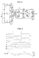
- FIG. 1 is a circuit diagram illustrating an embodiment of the present invention.
- DC unit power sources b1 and b2 each having a voltage of 2E V are connected in series, thereby constituting a DC combined power source BA1.
- External terminals of an arm pair QA1 composed of series-connected semiconductor switches Q1, Q2 are connected to a positive terminal and an intermediate terminal, respectively, of the DC combined power source BA1, and external terminals of an arm pair QA2 composed of series-connected semiconductor switches Q3, Q4 are connected to the intermediate terminal and a negative terminal, respectively.
- External terminals of an arm pair QA3 composed of series-connected semiconductor switches Q5, Q6 are respectively connected to the mid-point terminals of the arm pairs QA1 and QA2, and the mid-point terminal thereof serves as an AC output point U.
- a series capacitor circuit CA1 composed of capacitors C1, C2 is connected in parallel with the external terminals of the arm pair QA3, and an AC switch SW1 composed of semiconductor switches Q11, Q12 is connected between the intermediate connection point of the capacitors C1 and C2 and the mid-point terminal of QA3.
- FIG. 6 shows an ON-OFF pattern of semiconductor switches Q1 to Q6, Q11, and Q12 and a voltage waveform at the AC output point U in this case.
- the capacitors C1, C2 have the same capacity and the operation of semiconductor switches Q1 and Q4, Q2 and Q3, Q5 and Q6, and Q11 and Q12 is symmetrical in the positive-negative periods, as shown in FIG. 6 , both the voltage and the AC output current at the AC output point U will have positive-negative symmetry.
- FIG. 2 shows a variation example of the configuration shown in FIG. 1 .
- the difference between this example and that shown in FIG. 1 is that the reverse series connection of the semiconductor switches Q11 and Q12 constituting the AC switch SW1 is changed to a reverse parallel connection of Q21 and Q22 based on reverse blocking IGBTs.
- Such a change causes no changes in operational functions and the operations are performed in exactly the same manner as in the configuration shown in FIG. 1 .
- an output current passes through SW1
- the current passes only through either of Q21 and Q22 in the configuration shown in FIG. 2
- the current passes through both Q11 and Q12.
- the maximum number of semiconductor switches (including reverse blocking IGBTs) through which the output current passes in the entire five-level converter is reduced from three to two, thereby enabling further improvement of efficiency.
- FIG. 3 shows a first variation example of the configuration shown in FIG. 2 .
- the difference between this example and that shown in FIG. 2 is that windings La, Lb of a coupling reactor L1 are connected between the series capacitor circuit CA1 and arm pairs QA1, QA2, respectively.
- the operation of the circuit shown in FIG. 3 is similar to that shown in FIG. 2 and the explanation thereof is omitted.
- the connection destination of the series capacitor circuit CA1 is switched to the unit power source b1 or b2 by a switching operation of Q1 to Q4 at timings of points a and b, as shown in FIG. 6 .
- an inrush current created by this difference in electric potential is generated in the series capacitor circuit CA1.
- the inrush current to the series capacitor circuit CA1 is inhibited by inserting the coupling reactor L1 as shown in FIG. 3 .
- the reactor L1 is configured as a coupling reactor composed of windings La, Lb, the impedance with respect to the inrush current to the series capacitor circuit CA1 is raised, the inhibition effect thereof is increased, and the output impedance with respect to the output U is reduced.
- PWM control of Q1 or Q2 rather than simply switching Q1 and Q2 ON-OFF at the timings of points a and b in FIG. 6 under a voltage condition of b1 > b2, it is possible to inhibit completely the inrush current created by the difference in voltage at b1, b2, and CA1.
- the inrush current can be inhibited by the PWM control of Q3, Q4.
- FIG. 4 shows the second variation example of the configuration shown in FIG. 2 .
- a voltage balance circuit VB1 composed of Q7, Q8, and a reactor L2 is additionally provided to balance the voltages of capacitors C1, C2 of the series capacitor circuit CA1.
- the voltage balance circuit VB1 is added to the circuit shown in FIG. 3 .
- the operation of the configuration obtained is similar to that of the configuration shown in FIG. 4 and the explanation thereof is herein omitted.
Landscapes
- Engineering & Computer Science (AREA)
- Power Engineering (AREA)
- Inverter Devices (AREA)
- Dc-Dc Converters (AREA)
- Rectifiers (AREA)
Applications Claiming Priority (1)
| Application Number | Priority Date | Filing Date | Title |
|---|---|---|---|
| JP2009220665A JP5593660B2 (ja) | 2009-09-25 | 2009-09-25 | 5レベルインバータ |
Publications (3)
| Publication Number | Publication Date |
|---|---|
| EP2306629A2 true EP2306629A2 (fr) | 2011-04-06 |
| EP2306629A3 EP2306629A3 (fr) | 2011-06-22 |
| EP2306629B1 EP2306629B1 (fr) | 2014-07-30 |
Family
ID=43606392
Family Applications (1)
| Application Number | Title | Priority Date | Filing Date |
|---|---|---|---|
| EP10177221.8A Not-in-force EP2306629B1 (fr) | 2009-09-25 | 2010-09-16 | Convertisseur à cinq niveaux |
Country Status (3)
| Country | Link |
|---|---|
| EP (1) | EP2306629B1 (fr) |
| JP (1) | JP5593660B2 (fr) |
| CN (1) | CN102035420B (fr) |
Cited By (14)
| Publication number | Priority date | Publication date | Assignee | Title |
|---|---|---|---|---|
| CN102624267A (zh) * | 2012-03-27 | 2012-08-01 | 阳光电源股份有限公司 | 逆变器及其在三相系统中的应用电路 |
| JP2013021891A (ja) * | 2011-07-14 | 2013-01-31 | Mitsubishi Electric Corp | 電力変換装置 |
| US20130270917A1 (en) * | 2012-04-13 | 2013-10-17 | Fuji Electric Co., Ltd. | Multilevel power converter |
| EP2698911A4 (fr) * | 2012-05-25 | 2015-01-21 | Huawei Tech Co Ltd | Circuit électronique de puissance |
| CN105226978A (zh) * | 2015-10-10 | 2016-01-06 | 阳光电源股份有限公司 | 一种五电平逆变器及其应用电路 |
| WO2016146171A1 (fr) * | 2015-03-17 | 2016-09-22 | Siemens Aktiengesellschaft | Redresseur de haut rendement pour systèmes monophasés |
| EP2747269A3 (fr) * | 2012-12-19 | 2017-11-22 | General Electric Company | Convertisseur multi-cellules |
| DE102016224312A1 (de) | 2016-12-07 | 2018-06-07 | Siemens Aktiengesellschaft | Hocheffizienter Stromrichter für dreiphasige Systeme |
| DE102016224310A1 (de) | 2016-12-07 | 2018-06-07 | Siemens Aktiengesellschaft | Hocheffizienter Stromrichter für einphasige Systeme |
| DE102019201630A1 (de) * | 2019-02-08 | 2020-08-13 | Siemens Aktiengesellschaft | Hocheffizienter Stromrichter für einphasige und dreiphasige Systeme |
| WO2021038158A1 (fr) * | 2019-08-30 | 2021-03-04 | Socomec | Convertisseur modulaire multiniveaux pour application basse tension avec dimensionnement optimise des condensateurs |
| WO2021160529A1 (fr) | 2020-02-13 | 2021-08-19 | Siemens Aktiengesellschaft | Circuit convertisseur de courant |
| DE102021108250A1 (de) | 2021-03-31 | 2022-10-06 | KEBA Energy Automation GmbH | Ladestation und Verfahren zum Betreiben einer Ladestation |
| WO2026013600A1 (fr) * | 2024-07-10 | 2026-01-15 | dcbel Inc. | Convertisseur de puissance |
Families Citing this family (12)
| Publication number | Priority date | Publication date | Assignee | Title |
|---|---|---|---|---|
| JP5682459B2 (ja) * | 2011-06-07 | 2015-03-11 | 富士電機株式会社 | 5レベル変換回路 |
| CN110022078B (zh) | 2012-03-30 | 2021-05-04 | 富士电机株式会社 | 电力变换装置 |
| JP5910334B2 (ja) * | 2012-06-11 | 2016-04-27 | 株式会社明電舎 | 5レベル電力変換器 |
| JP5910333B2 (ja) * | 2012-06-11 | 2016-04-27 | 株式会社明電舎 | 5レベル電力変換器 |
| JP5598513B2 (ja) * | 2012-08-29 | 2014-10-01 | 株式会社村田製作所 | 電力系統連系インバータ装置 |
| JP5872494B2 (ja) * | 2013-01-24 | 2016-03-01 | 株式会社東芝 | 車両用電力変換装置 |
| US9941813B2 (en) | 2013-03-14 | 2018-04-10 | Solaredge Technologies Ltd. | High frequency multi-level inverter |
| CN103259436B (zh) * | 2013-05-21 | 2015-08-19 | 合肥工业大学 | 混合箝位型五电平变流器及其控制方法 |
| US9537425B2 (en) | 2013-07-09 | 2017-01-03 | Transphorm Inc. | Multilevel inverters and their components |
| US9318974B2 (en) | 2014-03-26 | 2016-04-19 | Solaredge Technologies Ltd. | Multi-level inverter with flying capacitor topology |
| WO2016065012A1 (fr) * | 2014-10-22 | 2016-04-28 | Otis Elevator Company | Convertisseur d'énergie npc de type t à trois niveaux |
| US12334839B2 (en) * | 2022-03-05 | 2025-06-17 | Hamilton Sundstrand Corporation | Power converter having diode bridges in parallel with interconnect switching module |
Citations (1)
| Publication number | Priority date | Publication date | Assignee | Title |
|---|---|---|---|---|
| JP2006271042A (ja) | 2005-03-23 | 2006-10-05 | Fuji Electric Holdings Co Ltd | マルチレベルインバータ |
Family Cites Families (11)
| Publication number | Priority date | Publication date | Assignee | Title |
|---|---|---|---|---|
| JPH05211776A (ja) * | 1992-01-31 | 1993-08-20 | Fuji Electric Co Ltd | インバータ |
| EP0727870B1 (fr) * | 1995-02-14 | 2000-08-30 | Kabushiki Kaisha Toshiba | Convertisseur de puissance |
| JPH08289474A (ja) * | 1995-04-18 | 1996-11-01 | Meidensha Corp | パワーラインコンディショナ |
| JP3249380B2 (ja) * | 1995-06-13 | 2002-01-21 | 株式会社東芝 | 電力変換装置 |
| JP4494562B2 (ja) * | 1999-09-28 | 2010-06-30 | 株式会社ダイヘン | 太陽光発電用電力変換装置 |
| JP2002247862A (ja) * | 2001-02-20 | 2002-08-30 | Hitachi Ltd | 電力変換装置 |
| DE10131961A1 (de) * | 2001-07-02 | 2003-01-23 | Siemens Ag | N-Punkt-Stromrichterschaltung |
| JP3651796B2 (ja) * | 2002-08-05 | 2005-05-25 | 株式会社東芝 | 電力変換装置 |
| CN100386959C (zh) * | 2004-12-16 | 2008-05-07 | 西安交通大学 | 五电平高频直流变换装置 |
| JP2007028860A (ja) * | 2005-07-21 | 2007-02-01 | Hitachi Ltd | 電力変換装置及びこれを備えた鉄道車輌 |
| CN2894074Y (zh) * | 2006-04-17 | 2007-04-25 | 山东新风光电子科技发展有限公司 | 一种五电平变换器结构装置 |
-
2009
- 2009-09-25 JP JP2009220665A patent/JP5593660B2/ja not_active Expired - Fee Related
-
2010
- 2010-09-01 CN CN2010102762980A patent/CN102035420B/zh not_active Expired - Fee Related
- 2010-09-16 EP EP10177221.8A patent/EP2306629B1/fr not_active Not-in-force
Patent Citations (1)
| Publication number | Priority date | Publication date | Assignee | Title |
|---|---|---|---|---|
| JP2006271042A (ja) | 2005-03-23 | 2006-10-05 | Fuji Electric Holdings Co Ltd | マルチレベルインバータ |
Non-Patent Citations (1)
| Title |
|---|
| "A multilevel voltage-source converter system with balanced DC voltage", IEEE-PESC95 CONFERENCE RECORD, pages 1144 - 1150 |
Cited By (23)
| Publication number | Priority date | Publication date | Assignee | Title |
|---|---|---|---|---|
| JP2013021891A (ja) * | 2011-07-14 | 2013-01-31 | Mitsubishi Electric Corp | 電力変換装置 |
| CN102624267B (zh) * | 2012-03-27 | 2014-07-16 | 阳光电源股份有限公司 | 逆变器及其在三相系统中的应用电路 |
| CN102624267A (zh) * | 2012-03-27 | 2012-08-01 | 阳光电源股份有限公司 | 逆变器及其在三相系统中的应用电路 |
| US20130270917A1 (en) * | 2012-04-13 | 2013-10-17 | Fuji Electric Co., Ltd. | Multilevel power converter |
| US9142956B2 (en) | 2012-04-13 | 2015-09-22 | Fuji Electric Co., Ltd. | Multilevel power converter |
| EP2698911A4 (fr) * | 2012-05-25 | 2015-01-21 | Huawei Tech Co Ltd | Circuit électronique de puissance |
| EP2747269A3 (fr) * | 2012-12-19 | 2017-11-22 | General Electric Company | Convertisseur multi-cellules |
| WO2016146171A1 (fr) * | 2015-03-17 | 2016-09-22 | Siemens Aktiengesellschaft | Redresseur de haut rendement pour systèmes monophasés |
| US10084392B2 (en) | 2015-10-10 | 2018-09-25 | Sungrow Power Supply Co., Ltd. | Five-level inverter and application circuit of the same |
| CN105226978A (zh) * | 2015-10-10 | 2016-01-06 | 阳光电源股份有限公司 | 一种五电平逆变器及其应用电路 |
| CN105226978B (zh) * | 2015-10-10 | 2018-04-10 | 阳光电源股份有限公司 | 一种五电平逆变器及其应用电路 |
| DE102016224312A1 (de) | 2016-12-07 | 2018-06-07 | Siemens Aktiengesellschaft | Hocheffizienter Stromrichter für dreiphasige Systeme |
| WO2018104174A1 (fr) | 2016-12-07 | 2018-06-14 | Siemens Aktiengesellschaft | Convertisseur à haut rendement pour systèmes monophasés |
| WO2018104177A1 (fr) | 2016-12-07 | 2018-06-14 | Siemens Aktiengesellschaft | Convertisseur à haut rendement pour systèmes triphasés |
| DE102016224310A1 (de) | 2016-12-07 | 2018-06-07 | Siemens Aktiengesellschaft | Hocheffizienter Stromrichter für einphasige Systeme |
| DE102019201630A1 (de) * | 2019-02-08 | 2020-08-13 | Siemens Aktiengesellschaft | Hocheffizienter Stromrichter für einphasige und dreiphasige Systeme |
| WO2021038158A1 (fr) * | 2019-08-30 | 2021-03-04 | Socomec | Convertisseur modulaire multiniveaux pour application basse tension avec dimensionnement optimise des condensateurs |
| FR3100403A1 (fr) * | 2019-08-30 | 2021-03-05 | Socomec | Convertisseur modulaire multiniveaux pour application basse tension avec dimensionnement optimisé des condensateurs |
| WO2021160529A1 (fr) | 2020-02-13 | 2021-08-19 | Siemens Aktiengesellschaft | Circuit convertisseur de courant |
| DE102020201810A1 (de) | 2020-02-13 | 2021-08-19 | Siemens Aktiengesellschaft | Stromrichter-Schaltung |
| DE102020201810B4 (de) | 2020-02-13 | 2023-01-12 | Siemens Aktiengesellschaft | Stromrichter-Schaltung |
| DE102021108250A1 (de) | 2021-03-31 | 2022-10-06 | KEBA Energy Automation GmbH | Ladestation und Verfahren zum Betreiben einer Ladestation |
| WO2026013600A1 (fr) * | 2024-07-10 | 2026-01-15 | dcbel Inc. | Convertisseur de puissance |
Also Published As
| Publication number | Publication date |
|---|---|
| EP2306629B1 (fr) | 2014-07-30 |
| JP5593660B2 (ja) | 2014-09-24 |
| CN102035420A (zh) | 2011-04-27 |
| EP2306629A3 (fr) | 2011-06-22 |
| JP2011072118A (ja) | 2011-04-07 |
| CN102035420B (zh) | 2013-10-16 |
Similar Documents
| Publication | Publication Date | Title |
|---|---|---|
| EP2306629A2 (fr) | Convertisseur à cinq niveaux | |
| EP2251969B1 (fr) | Onduleur à cinq niveaux | |
| JP5974516B2 (ja) | 5レベル電力変換装置 | |
| CN103378758B (zh) | 多电平电力转换器 | |
| JP5644944B2 (ja) | マルチレベル変換回路 | |
| US10447173B2 (en) | Single-phase five-level active clamping converter unit and converter | |
| KR101189428B1 (ko) | 전력 변환 장치 | |
| CN102884722B (zh) | 多电平逆变器 | |
| JP2013223274A5 (fr) | ||
| JP5803683B2 (ja) | マルチレベル電力変換回路 | |
| CN104335473B (zh) | 高压高功率多电平驱动器结构 | |
| JP6079407B2 (ja) | マルチレベル変換回路 | |
| JP5682459B2 (ja) | 5レベル変換回路 | |
| JP2012191761A (ja) | 交流−直流変換回路 | |
| JP2014161148A (ja) | マルチレベル電力変換回路の制御方式 | |
| CN106067723A (zh) | 切换模块和具有至少一个切换模块的转换器 | |
| JP7457240B2 (ja) | 電力変換装置及びそれを備えたモータ模擬装置 | |
| CN105375799A (zh) | 具有dc故障电流限制能力的模块化多电平功率变换系统 | |
| JP2013258863A (ja) | マルチレベル電力変換器 | |
| JP7054816B2 (ja) | 電力変換装置 | |
| JP7175649B2 (ja) | 三相電力変換装置及び無停電電源装置 |
Legal Events
| Date | Code | Title | Description |
|---|---|---|---|
| PUAI | Public reference made under article 153(3) epc to a published international application that has entered the european phase |
Free format text: ORIGINAL CODE: 0009012 |
|
| 17P | Request for examination filed |
Effective date: 20100916 |
|
| AK | Designated contracting states |
Kind code of ref document: A2 Designated state(s): AL AT BE BG CH CY CZ DE DK EE ES FI FR GB GR HR HU IE IS IT LI LT LU LV MC MK MT NL NO PL PT RO SE SI SK SM TR |
|
| AX | Request for extension of the european patent |
Extension state: BA ME RS |
|
| PUAL | Search report despatched |
Free format text: ORIGINAL CODE: 0009013 |
|
| AK | Designated contracting states |
Kind code of ref document: A3 Designated state(s): AL AT BE BG CH CY CZ DE DK EE ES FI FR GB GR HR HU IE IS IT LI LT LU LV MC MK MT NL NO PL PT RO SE SI SK SM TR |
|
| AX | Request for extension of the european patent |
Extension state: BA ME RS |
|
| RIC1 | Information provided on ipc code assigned before grant |
Ipc: H02M 7/487 20070101ALI20110513BHEP Ipc: H02M 7/483 20070101AFI20110225BHEP |
|
| RAP1 | Party data changed (applicant data changed or rights of an application transferred) |
Owner name: FUJI ELECTRIC CO., LTD. |
|
| RIC1 | Information provided on ipc code assigned before grant |
Ipc: H02M 7/487 20070101ALI20131114BHEP Ipc: H02M 7/483 20070101AFI20131114BHEP |
|
| GRAP | Despatch of communication of intention to grant a patent |
Free format text: ORIGINAL CODE: EPIDOSNIGR1 |
|
| INTG | Intention to grant announced |
Effective date: 20140210 |
|
| GRAS | Grant fee paid |
Free format text: ORIGINAL CODE: EPIDOSNIGR3 |
|
| GRAA | (expected) grant |
Free format text: ORIGINAL CODE: 0009210 |
|
| AK | Designated contracting states |
Kind code of ref document: B1 Designated state(s): AL AT BE BG CH CY CZ DE DK EE ES FI FR GB GR HR HU IE IS IT LI LT LU LV MC MK MT NL NO PL PT RO SE SI SK SM TR |
|
| REG | Reference to a national code |
Ref country code: GB Ref legal event code: FG4D |
|
| REG | Reference to a national code |
Ref country code: CH Ref legal event code: EP |
|
| REG | Reference to a national code |
Ref country code: AT Ref legal event code: REF Ref document number: 680362 Country of ref document: AT Kind code of ref document: T Effective date: 20140815 |
|
| REG | Reference to a national code |
Ref country code: IE Ref legal event code: FG4D |
|
| REG | Reference to a national code |
Ref country code: DE Ref legal event code: R096 Ref document number: 602010017853 Country of ref document: DE Effective date: 20140911 |
|
| REG | Reference to a national code |
Ref country code: AT Ref legal event code: MK05 Ref document number: 680362 Country of ref document: AT Kind code of ref document: T Effective date: 20140730 |
|
| REG | Reference to a national code |
Ref country code: NL Ref legal event code: VDEP Effective date: 20140730 |
|
| REG | Reference to a national code |
Ref country code: LT Ref legal event code: MG4D |
|
| PG25 | Lapsed in a contracting state [announced via postgrant information from national office to epo] |
Ref country code: BG Free format text: LAPSE BECAUSE OF FAILURE TO SUBMIT A TRANSLATION OF THE DESCRIPTION OR TO PAY THE FEE WITHIN THE PRESCRIBED TIME-LIMIT Effective date: 20141030 Ref country code: PT Free format text: LAPSE BECAUSE OF FAILURE TO SUBMIT A TRANSLATION OF THE DESCRIPTION OR TO PAY THE FEE WITHIN THE PRESCRIBED TIME-LIMIT Effective date: 20141202 Ref country code: SE Free format text: LAPSE BECAUSE OF FAILURE TO SUBMIT A TRANSLATION OF THE DESCRIPTION OR TO PAY THE FEE WITHIN THE PRESCRIBED TIME-LIMIT Effective date: 20140730 Ref country code: FI Free format text: LAPSE BECAUSE OF FAILURE TO SUBMIT A TRANSLATION OF THE DESCRIPTION OR TO PAY THE FEE WITHIN THE PRESCRIBED TIME-LIMIT Effective date: 20140730 Ref country code: GR Free format text: LAPSE BECAUSE OF FAILURE TO SUBMIT A TRANSLATION OF THE DESCRIPTION OR TO PAY THE FEE WITHIN THE PRESCRIBED TIME-LIMIT Effective date: 20141031 Ref country code: LT Free format text: LAPSE BECAUSE OF FAILURE TO SUBMIT A TRANSLATION OF THE DESCRIPTION OR TO PAY THE FEE WITHIN THE PRESCRIBED TIME-LIMIT Effective date: 20140730 Ref country code: ES Free format text: LAPSE BECAUSE OF FAILURE TO SUBMIT A TRANSLATION OF THE DESCRIPTION OR TO PAY THE FEE WITHIN THE PRESCRIBED TIME-LIMIT Effective date: 20140730 Ref country code: NO Free format text: LAPSE BECAUSE OF FAILURE TO SUBMIT A TRANSLATION OF THE DESCRIPTION OR TO PAY THE FEE WITHIN THE PRESCRIBED TIME-LIMIT Effective date: 20141030 |
|
| PG25 | Lapsed in a contracting state [announced via postgrant information from national office to epo] |
Ref country code: CY Free format text: LAPSE BECAUSE OF FAILURE TO SUBMIT A TRANSLATION OF THE DESCRIPTION OR TO PAY THE FEE WITHIN THE PRESCRIBED TIME-LIMIT Effective date: 20140730 Ref country code: HR Free format text: LAPSE BECAUSE OF FAILURE TO SUBMIT A TRANSLATION OF THE DESCRIPTION OR TO PAY THE FEE WITHIN THE PRESCRIBED TIME-LIMIT Effective date: 20140730 Ref country code: IS Free format text: LAPSE BECAUSE OF FAILURE TO SUBMIT A TRANSLATION OF THE DESCRIPTION OR TO PAY THE FEE WITHIN THE PRESCRIBED TIME-LIMIT Effective date: 20141130 Ref country code: PL Free format text: LAPSE BECAUSE OF FAILURE TO SUBMIT A TRANSLATION OF THE DESCRIPTION OR TO PAY THE FEE WITHIN THE PRESCRIBED TIME-LIMIT Effective date: 20140730 Ref country code: NL Free format text: LAPSE BECAUSE OF FAILURE TO SUBMIT A TRANSLATION OF THE DESCRIPTION OR TO PAY THE FEE WITHIN THE PRESCRIBED TIME-LIMIT Effective date: 20140730 Ref country code: AT Free format text: LAPSE BECAUSE OF FAILURE TO SUBMIT A TRANSLATION OF THE DESCRIPTION OR TO PAY THE FEE WITHIN THE PRESCRIBED TIME-LIMIT Effective date: 20140730 Ref country code: LV Free format text: LAPSE BECAUSE OF FAILURE TO SUBMIT A TRANSLATION OF THE DESCRIPTION OR TO PAY THE FEE WITHIN THE PRESCRIBED TIME-LIMIT Effective date: 20140730 |
|
| PG25 | Lapsed in a contracting state [announced via postgrant information from national office to epo] |
Ref country code: LU Free format text: LAPSE BECAUSE OF FAILURE TO SUBMIT A TRANSLATION OF THE DESCRIPTION OR TO PAY THE FEE WITHIN THE PRESCRIBED TIME-LIMIT Effective date: 20140916 Ref country code: EE Free format text: LAPSE BECAUSE OF FAILURE TO SUBMIT A TRANSLATION OF THE DESCRIPTION OR TO PAY THE FEE WITHIN THE PRESCRIBED TIME-LIMIT Effective date: 20140730 Ref country code: RO Free format text: LAPSE BECAUSE OF FAILURE TO SUBMIT A TRANSLATION OF THE DESCRIPTION OR TO PAY THE FEE WITHIN THE PRESCRIBED TIME-LIMIT Effective date: 20140730 Ref country code: DK Free format text: LAPSE BECAUSE OF FAILURE TO SUBMIT A TRANSLATION OF THE DESCRIPTION OR TO PAY THE FEE WITHIN THE PRESCRIBED TIME-LIMIT Effective date: 20140730 Ref country code: CZ Free format text: LAPSE BECAUSE OF FAILURE TO SUBMIT A TRANSLATION OF THE DESCRIPTION OR TO PAY THE FEE WITHIN THE PRESCRIBED TIME-LIMIT Effective date: 20140730 Ref country code: SK Free format text: LAPSE BECAUSE OF FAILURE TO SUBMIT A TRANSLATION OF THE DESCRIPTION OR TO PAY THE FEE WITHIN THE PRESCRIBED TIME-LIMIT Effective date: 20140730 Ref country code: IT Free format text: LAPSE BECAUSE OF FAILURE TO SUBMIT A TRANSLATION OF THE DESCRIPTION OR TO PAY THE FEE WITHIN THE PRESCRIBED TIME-LIMIT Effective date: 20140730 Ref country code: MC Free format text: LAPSE BECAUSE OF FAILURE TO SUBMIT A TRANSLATION OF THE DESCRIPTION OR TO PAY THE FEE WITHIN THE PRESCRIBED TIME-LIMIT Effective date: 20140730 |
|
| REG | Reference to a national code |
Ref country code: DE Ref legal event code: R097 Ref document number: 602010017853 Country of ref document: DE |
|
| PLBE | No opposition filed within time limit |
Free format text: ORIGINAL CODE: 0009261 |
|
| STAA | Information on the status of an ep patent application or granted ep patent |
Free format text: STATUS: NO OPPOSITION FILED WITHIN TIME LIMIT |
|
| REG | Reference to a national code |
Ref country code: IE Ref legal event code: MM4A |
|
| GBPC | Gb: european patent ceased through non-payment of renewal fee |
Effective date: 20141030 |
|
| PG25 | Lapsed in a contracting state [announced via postgrant information from national office to epo] |
Ref country code: BE Free format text: LAPSE BECAUSE OF NON-PAYMENT OF DUE FEES Effective date: 20140930 |
|
| 26N | No opposition filed |
Effective date: 20150504 |
|
| PG25 | Lapsed in a contracting state [announced via postgrant information from national office to epo] |
Ref country code: GB Free format text: LAPSE BECAUSE OF NON-PAYMENT OF DUE FEES Effective date: 20141030 |
|
| PG25 | Lapsed in a contracting state [announced via postgrant information from national office to epo] |
Ref country code: IE Free format text: LAPSE BECAUSE OF NON-PAYMENT OF DUE FEES Effective date: 20140916 |
|
| PG25 | Lapsed in a contracting state [announced via postgrant information from national office to epo] |
Ref country code: SI Free format text: LAPSE BECAUSE OF FAILURE TO SUBMIT A TRANSLATION OF THE DESCRIPTION OR TO PAY THE FEE WITHIN THE PRESCRIBED TIME-LIMIT Effective date: 20140730 |
|
| PG25 | Lapsed in a contracting state [announced via postgrant information from national office to epo] |
Ref country code: SM Free format text: LAPSE BECAUSE OF FAILURE TO SUBMIT A TRANSLATION OF THE DESCRIPTION OR TO PAY THE FEE WITHIN THE PRESCRIBED TIME-LIMIT Effective date: 20140730 |
|
| PG25 | Lapsed in a contracting state [announced via postgrant information from national office to epo] |
Ref country code: MT Free format text: LAPSE BECAUSE OF FAILURE TO SUBMIT A TRANSLATION OF THE DESCRIPTION OR TO PAY THE FEE WITHIN THE PRESCRIBED TIME-LIMIT Effective date: 20140730 |
|
| PG25 | Lapsed in a contracting state [announced via postgrant information from national office to epo] |
Ref country code: BE Free format text: LAPSE BECAUSE OF FAILURE TO SUBMIT A TRANSLATION OF THE DESCRIPTION OR TO PAY THE FEE WITHIN THE PRESCRIBED TIME-LIMIT Effective date: 20140730 Ref country code: HU Free format text: LAPSE BECAUSE OF FAILURE TO SUBMIT A TRANSLATION OF THE DESCRIPTION OR TO PAY THE FEE WITHIN THE PRESCRIBED TIME-LIMIT; INVALID AB INITIO Effective date: 20100916 Ref country code: TR Free format text: LAPSE BECAUSE OF FAILURE TO SUBMIT A TRANSLATION OF THE DESCRIPTION OR TO PAY THE FEE WITHIN THE PRESCRIBED TIME-LIMIT Effective date: 20140730 |
|
| REG | Reference to a national code |
Ref country code: FR Ref legal event code: PLFP Year of fee payment: 7 |
|
| REG | Reference to a national code |
Ref country code: FR Ref legal event code: PLFP Year of fee payment: 8 |
|
| PG25 | Lapsed in a contracting state [announced via postgrant information from national office to epo] |
Ref country code: MK Free format text: LAPSE BECAUSE OF FAILURE TO SUBMIT A TRANSLATION OF THE DESCRIPTION OR TO PAY THE FEE WITHIN THE PRESCRIBED TIME-LIMIT Effective date: 20140730 |
|
| REG | Reference to a national code |
Ref country code: FR Ref legal event code: PLFP Year of fee payment: 9 |
|
| PG25 | Lapsed in a contracting state [announced via postgrant information from national office to epo] |
Ref country code: AL Free format text: LAPSE BECAUSE OF FAILURE TO SUBMIT A TRANSLATION OF THE DESCRIPTION OR TO PAY THE FEE WITHIN THE PRESCRIBED TIME-LIMIT Effective date: 20140730 |
|
| PGFP | Annual fee paid to national office [announced via postgrant information from national office to epo] |
Ref country code: DE Payment date: 20180904 Year of fee payment: 9 Ref country code: FR Payment date: 20180813 Year of fee payment: 9 |
|
| PGFP | Annual fee paid to national office [announced via postgrant information from national office to epo] |
Ref country code: CH Payment date: 20180913 Year of fee payment: 9 |
|
| REG | Reference to a national code |
Ref country code: DE Ref legal event code: R119 Ref document number: 602010017853 Country of ref document: DE |
|
| REG | Reference to a national code |
Ref country code: CH Ref legal event code: PL |
|
| PG25 | Lapsed in a contracting state [announced via postgrant information from national office to epo] |
Ref country code: LI Free format text: LAPSE BECAUSE OF NON-PAYMENT OF DUE FEES Effective date: 20190930 Ref country code: DE Free format text: LAPSE BECAUSE OF NON-PAYMENT OF DUE FEES Effective date: 20200401 Ref country code: CH Free format text: LAPSE BECAUSE OF NON-PAYMENT OF DUE FEES Effective date: 20190930 |
|
| PG25 | Lapsed in a contracting state [announced via postgrant information from national office to epo] |
Ref country code: FR Free format text: LAPSE BECAUSE OF NON-PAYMENT OF DUE FEES Effective date: 20190930 |