EP2309538A2 - Verpackung für Halbleiterbauelemente - Google Patents
Verpackung für Halbleiterbauelemente Download PDFInfo
- Publication number
- EP2309538A2 EP2309538A2 EP10251762A EP10251762A EP2309538A2 EP 2309538 A2 EP2309538 A2 EP 2309538A2 EP 10251762 A EP10251762 A EP 10251762A EP 10251762 A EP10251762 A EP 10251762A EP 2309538 A2 EP2309538 A2 EP 2309538A2
- Authority
- EP
- European Patent Office
- Prior art keywords
- semiconductor layer
- die
- header
- spaced external
- leadframe
- Prior art date
- Legal status (The legal status is an assumption and is not a legal conclusion. Google has not performed a legal analysis and makes no representation as to the accuracy of the status listed.)
- Withdrawn
Links
Images


Classifications
-
- H—ELECTRICITY
- H10—SEMICONDUCTOR DEVICES; ELECTRIC SOLID-STATE DEVICES NOT OTHERWISE PROVIDED FOR
- H10W—GENERIC PACKAGES, INTERCONNECTIONS, CONNECTORS OR OTHER CONSTRUCTIONAL DETAILS OF DEVICES COVERED BY CLASS H10
- H10W70/00—Package substrates; Interposers; Redistribution layers [RDL]
- H10W70/40—Leadframes
- H10W70/481—Leadframes for devices being provided for in groups H10D8/00 - H10D48/00
-
- H—ELECTRICITY
- H10—SEMICONDUCTOR DEVICES; ELECTRIC SOLID-STATE DEVICES NOT OTHERWISE PROVIDED FOR
- H10W—GENERIC PACKAGES, INTERCONNECTIONS, CONNECTORS OR OTHER CONSTRUCTIONAL DETAILS OF DEVICES COVERED BY CLASS H10
- H10W74/00—Encapsulations, e.g. protective coatings
- H10W74/10—Encapsulations, e.g. protective coatings characterised by their shape or disposition
- H10W74/111—Encapsulations, e.g. protective coatings characterised by their shape or disposition the semiconductor body being completely enclosed
-
- H—ELECTRICITY
- H10—SEMICONDUCTOR DEVICES; ELECTRIC SOLID-STATE DEVICES NOT OTHERWISE PROVIDED FOR
- H10W—GENERIC PACKAGES, INTERCONNECTIONS, CONNECTORS OR OTHER CONSTRUCTIONAL DETAILS OF DEVICES COVERED BY CLASS H10
- H10W42/00—Arrangements for protection of devices
- H10W42/121—Arrangements for protection of devices protecting against mechanical damage
-
- H—ELECTRICITY
- H10—SEMICONDUCTOR DEVICES; ELECTRIC SOLID-STATE DEVICES NOT OTHERWISE PROVIDED FOR
- H10W—GENERIC PACKAGES, INTERCONNECTIONS, CONNECTORS OR OTHER CONSTRUCTIONAL DETAILS OF DEVICES COVERED BY CLASS H10
- H10W72/00—Interconnections or connectors in packages
- H10W72/30—Die-attach connectors
- H10W72/351—Materials of die-attach connectors
- H10W72/353—Materials of die-attach connectors not comprising solid metals or solid metalloids, e.g. ceramics
- H10W72/354—Materials of die-attach connectors not comprising solid metals or solid metalloids, e.g. ceramics comprising polymers
-
- H—ELECTRICITY
- H10—SEMICONDUCTOR DEVICES; ELECTRIC SOLID-STATE DEVICES NOT OTHERWISE PROVIDED FOR
- H10W—GENERIC PACKAGES, INTERCONNECTIONS, CONNECTORS OR OTHER CONSTRUCTIONAL DETAILS OF DEVICES COVERED BY CLASS H10
- H10W72/00—Interconnections or connectors in packages
- H10W72/50—Bond wires
-
- H—ELECTRICITY
- H10—SEMICONDUCTOR DEVICES; ELECTRIC SOLID-STATE DEVICES NOT OTHERWISE PROVIDED FOR
- H10W—GENERIC PACKAGES, INTERCONNECTIONS, CONNECTORS OR OTHER CONSTRUCTIONAL DETAILS OF DEVICES COVERED BY CLASS H10
- H10W72/00—Interconnections or connectors in packages
- H10W72/50—Bond wires
- H10W72/531—Shapes of wire connectors
- H10W72/5363—Shapes of wire connectors the connected ends being wedge-shaped
-
- H—ELECTRICITY
- H10—SEMICONDUCTOR DEVICES; ELECTRIC SOLID-STATE DEVICES NOT OTHERWISE PROVIDED FOR
- H10W—GENERIC PACKAGES, INTERCONNECTIONS, CONNECTORS OR OTHER CONSTRUCTIONAL DETAILS OF DEVICES COVERED BY CLASS H10
- H10W72/00—Interconnections or connectors in packages
- H10W72/50—Bond wires
- H10W72/551—Materials of bond wires
- H10W72/552—Materials of bond wires comprising metals or metalloids, e.g. silver
- H10W72/5522—Materials of bond wires comprising metals or metalloids, e.g. silver comprising gold [Au]
-
- H—ELECTRICITY
- H10—SEMICONDUCTOR DEVICES; ELECTRIC SOLID-STATE DEVICES NOT OTHERWISE PROVIDED FOR
- H10W—GENERIC PACKAGES, INTERCONNECTIONS, CONNECTORS OR OTHER CONSTRUCTIONAL DETAILS OF DEVICES COVERED BY CLASS H10
- H10W72/00—Interconnections or connectors in packages
- H10W72/50—Bond wires
- H10W72/551—Materials of bond wires
- H10W72/552—Materials of bond wires comprising metals or metalloids, e.g. silver
- H10W72/5524—Materials of bond wires comprising metals or metalloids, e.g. silver comprising aluminium [Al]
-
- H—ELECTRICITY
- H10—SEMICONDUCTOR DEVICES; ELECTRIC SOLID-STATE DEVICES NOT OTHERWISE PROVIDED FOR
- H10W—GENERIC PACKAGES, INTERCONNECTIONS, CONNECTORS OR OTHER CONSTRUCTIONAL DETAILS OF DEVICES COVERED BY CLASS H10
- H10W72/00—Interconnections or connectors in packages
- H10W72/851—Dispositions of multiple connectors or interconnections
- H10W72/874—On different surfaces
- H10W72/884—Die-attach connectors and bond wires
-
- H—ELECTRICITY
- H10—SEMICONDUCTOR DEVICES; ELECTRIC SOLID-STATE DEVICES NOT OTHERWISE PROVIDED FOR
- H10W—GENERIC PACKAGES, INTERCONNECTIONS, CONNECTORS OR OTHER CONSTRUCTIONAL DETAILS OF DEVICES COVERED BY CLASS H10
- H10W74/00—Encapsulations, e.g. protective coatings
-
- H—ELECTRICITY
- H10—SEMICONDUCTOR DEVICES; ELECTRIC SOLID-STATE DEVICES NOT OTHERWISE PROVIDED FOR
- H10W—GENERIC PACKAGES, INTERCONNECTIONS, CONNECTORS OR OTHER CONSTRUCTIONAL DETAILS OF DEVICES COVERED BY CLASS H10
- H10W74/00—Encapsulations, e.g. protective coatings
- H10W74/01—Manufacture or treatment
-
- H—ELECTRICITY
- H10—SEMICONDUCTOR DEVICES; ELECTRIC SOLID-STATE DEVICES NOT OTHERWISE PROVIDED FOR
- H10W—GENERIC PACKAGES, INTERCONNECTIONS, CONNECTORS OR OTHER CONSTRUCTIONAL DETAILS OF DEVICES COVERED BY CLASS H10
- H10W90/00—Package configurations
- H10W90/701—Package configurations characterised by the relative positions of pads or connectors relative to package parts
- H10W90/731—Package configurations characterised by the relative positions of pads or connectors relative to package parts of die-attach connectors
- H10W90/736—Package configurations characterised by the relative positions of pads or connectors relative to package parts of die-attach connectors between a chip and a stacked lead frame, conducting package substrate or heat sink
-
- H—ELECTRICITY
- H10—SEMICONDUCTOR DEVICES; ELECTRIC SOLID-STATE DEVICES NOT OTHERWISE PROVIDED FOR
- H10W—GENERIC PACKAGES, INTERCONNECTIONS, CONNECTORS OR OTHER CONSTRUCTIONAL DETAILS OF DEVICES COVERED BY CLASS H10
- H10W90/00—Package configurations
- H10W90/701—Package configurations characterised by the relative positions of pads or connectors relative to package parts
- H10W90/751—Package configurations characterised by the relative positions of pads or connectors relative to package parts of bond wires
- H10W90/756—Package configurations characterised by the relative positions of pads or connectors relative to package parts of bond wires between a chip and a stacked lead frame, conducting package substrate or heat sink
Definitions
- the present invention relates to packaged semiconductor devices, and more particularly to a lead frame and package enclosing a high power gallium nitride based semiconductor device.
- Semiconductor devices such as diodes, field effect transistors and the like are commonly formed on semiconductor wafers/substrates which are later cut into dies containing individual devices or integrated circuits.
- the die has metallized pads or other electrodes which are electrically connected to source, gate, and drain regions in a transistor, or the anode and cathode in a diode.
- Most of the devices are formed on silicon (Si), silicon carbide (SiC), and gallium arsenide (GaAs) semiconductor wafers. All these substrates are electrically conducting which makes the devices made on such wafers “vertical devices", meaning they have electrical connections on the top and bottom surface of the die.
- a semiconductor die is mounted inside a package made of the copper leadframe and the encapsulating epoxy.
- packages used for power semiconductor devices are well known industry standards for example TO-220, TO-247, DPAK, D2PAK, TO-263 or other package form factors.
- the die is mounted onto the leadframe, which in turn provides electrical connection between the die and the bottom side of the package, and the mounting bracket on top of the encapsulated epoxy (in case of the TO220, TO247), and to at least one of the multiple external leads. Other electrical pads are connected to remaining external leads using wire bonds.
- die and parts of the leadframe are encapsulated with insulating epoxy. Due to this configuration the end user in many applications needs to use additional elements to provide sufficient electrical insulation between package and the external hardware (heat sink) or other equipment which increases the cost of the final product.
- U.S. Pat. No. 6,847,058 to Ishizaka et al. discloses a MOSFET as a semiconductor device.
- FIGS. 2 and 4 of Ishizaka shows the device having a die 1 fixed to an upper surface of the header 13 through a drain (D) electrode. All three leads, source (S), gate (G) and drain (D) are electrically connected to the die 1.
- the S and the G are connected via bonding wires 16 while the D is the back side of the die 1 and is always electrically and mechanically connected to the lead frame, thus requiring electrical insulation on the back side of the device.
- gallium nitride semiconductor devices for use in optoelectronic, power and other applications have presented new packaging requirements for such devices, while manufacturing economics considerations and the desire of customers for pin-compatible components have dictated that such packages still conform to industry accepted packaging formats.
- Embodiments of the present invention provide an improved electrical performance in a package for a semiconductor device.
- Embodiments of the present invention also provide a simplified and economically manufacturing assembly of the package for the semiconductor device.
- Embodiments of the invention also provide a package for a semiconductor device conforming to industry accepted packaging formats.
- the present invention provides a packaged semiconductor device including a semiconductor die mounted on a header of a leadframe.
- a plurality of spaced external conductors extends from the package and at least one of the external conductors has a bond wire pad/post at one end thereof such that a bonding wire extends between the bond wire pad/post and the semiconductor die.
- the packaged device also includes a housing, which encloses the semiconductor die, the header, the bonding wire(s) and the bonding wire pad(s)/post(s).
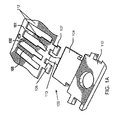
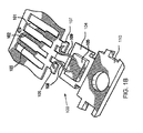
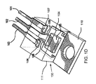
- FIGS. 1A-1D there is shown a set of fragmentary, perspective views of a sequence of the packaging of the semiconductor device 100 in accordance with the present invention.
- a typical leadframe, used in the packaging is illustrated in FIG. 1A . It consists of the mounting bracket 110 and a header 104 which also serves a mounting support for a die.
- the packaging device 100 also includes external leads or electrodes 101, 102, and 103 parallel to each other and held together via excess metal 112.
- the lead 102 is permanently connected to the header 104 via the metal extension 113.
- Each of the leads 103 and 101 further includes wire bonding pads/posts 106 and 107 respectively.
- FIG. 1B further includes a semiconductor die 105 mounted on the header 104. As shown in FIG.
- bonding wires 108 and 109 are used to make electrical connection between active regions on the top surface of the semiconductor die 105 and the wire-bonding pads/posts 106 and 107 on the leads 103 and 101 respectively. Due to the insulating nature of the substrate there is no electrical connection between the die and the header 104, hence no electrical connection to the lead 102 and the mounting bracket 110.
- FIG. 1C shows a housing 111 made of a moulded plastic material such as an epoxy which encapsulates the die 105 and the wires 108 and 109 and a portion of the leads 101 and 103 including the bonding pads/posts 106 and 107 respectively.
- the housing 111 also functions to provide mechanical support for the leads 101 and 103 once the excessive and/or unused metal 112 is cut-off as shown in FIG. 1D .
- FIG. 1D shows the final packaged semiconductor device 100 in which the excessive metal 112 is cut off such that the leads 101, 102 and 103 are independent and are no longer connected to each other via the metal 112. Also, by eliminating the excessive metal 112, the two outside leads 101 and 103 are not electrically connected to the header 104 and the mounting bracket 110. Thus, the final sealed packaged semiconductor device 100 in FIG. 10 provides complete insulation between the die 105 and the leadframe. Even though not displayed, the middle lead 102 may optionally be trimmed.
- the back side (not shown) of the header 104 remains uncovered which provides for a good thermal contact. This allows for the mounting of another element such as an external heat sink directly into the back side of the header 104 that would remove the heat generated in the die under normal operating conditions.
- the back side of the semiconductor packaged device is not isolated from the die and an insulator such as a Mylar film needs to be inserted between the device and the heat sink to avoid electrical connection between the two.
- an insulator is not required since the leads 101 and 103 are floating and clearly not connected to the backside of the sealed package device 100 resulting in an insulated packaged device.
- FIG. 2 there is shown a fragmentary, cross-sectional detail of the semiconductor GaN based diode structure 200 as the die 104 of FIG. 1 according to a preferred embodiment of the present invention.
- the structure 200 comprising a high power Gallium Nitride based diode 202 fabricated preferably on a sapphire (A1203) substrate 204.
- the diode 202 includes a highly doped (n+) layer 201 at the bottom and a lower doped (n-) layer 203 on top.
- an anode 206 is formed on the lowly doped (n-) layer 203 and a cathode 207 is formed only on the portions of the highly doped (n+) layer 201.
- a layer of dielectric 208 serves as a passivation to protect the die from the external elements (moisture, gases). It also provides electrical insulation between the two contacts.
- the anode 206 and a cathode 207 also serve as bonding pads on the die itself.
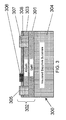
- FIG. 3 there is shown a fragmentary, cross-sectional detail of the GaN based field effect transistor (FET) structure 300 as the die 104 of FIG. 1 according to another preferred embodiment of the present invention.
- the structure 300 comprising a high power Gallium Nitride based FET 302 fabricated on the sapphire (A1203) substrate 304.
- the FET 302 includes GaN layer 301 at the bottom and the AIGaN layer 303 on top.
- a gate (G) electrode 306 is formed on the AlGaN layer 303 and the source (S) and drain (D) electrodes 305 and 307 respectively, are formed through the AlGaN layer 303 onto the GaN layer 301.
- a layer of dielectric 308 serves as a passivation to protect the die from the external elements. It also provides electrical insulation between the contacts. It is noted that the drawings on FIGS. 2 and 3 are for the illustration purposes only and are not too scale.
- GaN based devices shown are fabricated on a sapphire substrate, it is known to one skilled in the art that other semiconductor substrates like silicon (Si), silicon carbide (SiC) and like can be used.
- Sapphire substrates provide economical benefit comparing to silicon carbide substrates while at the same time enabling superior quality comparing to devices fabricated on silicon substrates. Additionally the sapphire substrates are electrically insulating, hence devices fabricated on such substrates will no longer be vertical devices.
- gallium nitride based devices fabricated on a sapphire substrate have all bonding pads on the upper surface of the die.
- a fully fabricated die on sapphire is attached to the leadframe with epoxy or soldered if earlier process steps include back side metallization, which might be beneficial for some applications. Electrical connections are made between the bonding pads and the external leads not connected to the leadframe, keeping the die electrically insulated from the frame. Later the die is encapsulated with epoxy and unused parts of the lead frame are cut off.
- multiple wires go from the die's bonding pads to external leads not connected to the header. Therefore, in case of the diode, there can be more than one bonding wire from the anode, and more than one bonding wire from the cathode, depending on the die configuration and type of bonding wire used.
- multiple GaN based devices can also be incorporated into one package, including any combination of diodes and FETs to meet the needs of integration and the industry. Wirebond connections may be made between those devices and between devices and external leads connected to the header. Any number of die can be included in the package, assuming that they will fit into the allotted space.
- two 0.25 mm (10 mil) aluminium wires are used.
- a 0.38 mm (15 mil) Al wires may preferably be used.
- the wire may be made of gold and be as small as 50 ⁇ m (2 mil).
- the method and device of the present invention described herein can thus be utilized in association with devices and/or other semiconductor device structures to improve reliability, control and stability thereof.
- the present invention thus applies to any semiconductor device utilizing mesa structures defining active regions, and in particular III-V semiconductor devices.
Landscapes
- Junction Field-Effect Transistors (AREA)
- Structures Or Materials For Encapsulating Or Coating Semiconductor Devices Or Solid State Devices (AREA)
- Lead Frames For Integrated Circuits (AREA)
Applications Claiming Priority (1)
| Application Number | Priority Date | Filing Date | Title |
|---|---|---|---|
| US12/575,717 US20100140627A1 (en) | 2005-01-10 | 2009-10-08 | Package for Semiconductor Devices |
Publications (2)
| Publication Number | Publication Date |
|---|---|
| EP2309538A2 true EP2309538A2 (de) | 2011-04-13 |
| EP2309538A3 EP2309538A3 (de) | 2012-12-26 |
Family
ID=43385677
Family Applications (1)
| Application Number | Title | Priority Date | Filing Date |
|---|---|---|---|
| EP10251762A Withdrawn EP2309538A3 (de) | 2009-10-08 | 2010-10-07 | Verpackung für Halbleiterbauelemente |
Country Status (5)
| Country | Link |
|---|---|
| US (1) | US20100140627A1 (de) |
| EP (1) | EP2309538A3 (de) |
| JP (1) | JP2011082523A (de) |
| CN (1) | CN102074539A (de) |
| TW (1) | TW201131722A (de) |
Families Citing this family (3)
| Publication number | Priority date | Publication date | Assignee | Title |
|---|---|---|---|---|
| JPWO2013047533A1 (ja) * | 2011-09-29 | 2015-03-26 | シャープ株式会社 | 半導体装置 |
| US9818677B2 (en) * | 2015-07-24 | 2017-11-14 | Semiconductor Components Industries, Llc | Semiconductor component having group III nitride semiconductor device mounted on substrate and interconnected to lead frame |
| CN110581105B (zh) * | 2019-07-30 | 2020-12-04 | 泉州台商投资区嘉尚网络科技有限公司 | 一种金属氧化物半导体粘结防挡光滑动的场效应管 |
Citations (1)
| Publication number | Priority date | Publication date | Assignee | Title |
|---|---|---|---|---|
| US6847058B2 (en) | 2002-09-12 | 2005-01-25 | Renesas Technology Corp. | Semiconductor device |
Family Cites Families (16)
| Publication number | Priority date | Publication date | Assignee | Title |
|---|---|---|---|---|
| US5111253A (en) * | 1989-05-09 | 1992-05-05 | General Electric Company | Multicellular FET having a Schottky diode merged therewith |
| DE19639025C2 (de) * | 1996-09-23 | 1999-10-28 | Siemens Ag | Chipmodul und Verfahren zur Herstellung eines Chipmoduls |
| JP2000049184A (ja) * | 1998-05-27 | 2000-02-18 | Hitachi Ltd | 半導体装置およびその製造方法 |
| US6335548B1 (en) * | 1999-03-15 | 2002-01-01 | Gentex Corporation | Semiconductor radiation emitter package |
| EP1277240B1 (de) * | 2000-04-26 | 2015-05-20 | OSRAM Opto Semiconductors GmbH | Verfahren zur Herstellung eines lichtmittierenden Halbleiterbauelements |
| US20030015708A1 (en) * | 2001-07-23 | 2003-01-23 | Primit Parikh | Gallium nitride based diodes with low forward voltage and low reverse current operation |
| US6740906B2 (en) * | 2001-07-23 | 2004-05-25 | Cree, Inc. | Light emitting diodes including modifications for submount bonding |
| US6975023B2 (en) * | 2002-09-04 | 2005-12-13 | International Rectifier Corporation | Co-packaged control circuit, transistor and inverted diode |
| JP4077731B2 (ja) * | 2003-01-27 | 2008-04-23 | 富士通株式会社 | 化合物半導体装置およびその製造方法 |
| FR2854498B1 (fr) * | 2003-04-29 | 2005-09-16 | St Microelectronics Sa | Boitier semi-conducteur a capteur optique s'installant a l'interieur d'un objet. |
| US7449728B2 (en) * | 2003-11-24 | 2008-11-11 | Tri Quint Semiconductor, Inc. | Monolithic integrated enhancement mode and depletion mode field effect transistors and method of making the same |
| US20050139838A1 (en) * | 2003-12-26 | 2005-06-30 | Matsushita Electric Industrial Co., Ltd. | Semiconductor device and method for manufacturing semiconductor device |
| JP4632690B2 (ja) * | 2004-05-11 | 2011-02-16 | スタンレー電気株式会社 | 半導体発光装置とその製造方法 |
| US7105875B2 (en) * | 2004-06-03 | 2006-09-12 | Wide Bandgap, Llc | Lateral power diodes |
| US20060151868A1 (en) * | 2005-01-10 | 2006-07-13 | Zhu Tinggang | Package for gallium nitride semiconductor devices |
| CN201011655Y (zh) * | 2007-01-10 | 2008-01-23 | 上海凯虹科技电子有限公司 | 一种大功率半导体器件的框架 |
-
2009
- 2009-10-08 US US12/575,717 patent/US20100140627A1/en not_active Abandoned
-
2010
- 2010-10-07 EP EP10251762A patent/EP2309538A3/de not_active Withdrawn
- 2010-10-08 JP JP2010228159A patent/JP2011082523A/ja active Pending
- 2010-10-08 CN CN2010105523479A patent/CN102074539A/zh active Pending
- 2010-10-08 TW TW099134488A patent/TW201131722A/zh unknown
Patent Citations (1)
| Publication number | Priority date | Publication date | Assignee | Title |
|---|---|---|---|---|
| US6847058B2 (en) | 2002-09-12 | 2005-01-25 | Renesas Technology Corp. | Semiconductor device |
Also Published As
| Publication number | Publication date |
|---|---|
| US20100140627A1 (en) | 2010-06-10 |
| CN102074539A (zh) | 2011-05-25 |
| JP2011082523A (ja) | 2011-04-21 |
| TW201131722A (en) | 2011-09-16 |
| EP2309538A3 (de) | 2012-12-26 |
Similar Documents
| Publication | Publication Date | Title |
|---|---|---|
| CN1819259B (zh) | 氮化镓半导体装置的封装 | |
| US8455987B1 (en) | Electrically isolated power semiconductor package with optimized layout | |
| US8629467B2 (en) | Semiconductor device | |
| US7582958B2 (en) | Semiconductor package | |
| US7800208B2 (en) | Device with a plurality of semiconductor chips | |
| US7443014B2 (en) | Electronic module and method of assembling the same | |
| CN217719586U (zh) | 电子器件 | |
| TW200913201A (en) | Dual side cooling integrated power device package and module and methods of manufacture | |
| US6433424B1 (en) | Semiconductor device package and lead frame with die overhanging lead frame pad | |
| CN113363231B (zh) | 半导体装置 | |
| US7375424B2 (en) | Wirebonded device packages for semiconductor devices having elongated electrodes | |
| US20230015323A1 (en) | Semiconductor package with topside cooling | |
| CN112635411A (zh) | 具有顶侧或底侧冷却的半导体封装 | |
| EP2309538A2 (de) | Verpackung für Halbleiterbauelemente | |
| US20250006603A1 (en) | Flip chip and pre-molded clip power modules | |
| US20240006364A1 (en) | Semiconductor device | |
| JPH09186288A (ja) | 半導体装置 | |
| US11069600B2 (en) | Semiconductor package with space efficient lead and die pad design | |
| CN114203659A (zh) | 多层互连带 | |
| US20130307131A1 (en) | Semiconductor device | |
| CN120221528A (zh) | 具有部件承载中间结构和带有参考电势结构的附加载体的封装体 | |
| JP2002110892A (ja) | マルチチップ半導体装置 |
Legal Events
| Date | Code | Title | Description |
|---|---|---|---|
| PUAI | Public reference made under article 153(3) epc to a published international application that has entered the european phase |
Free format text: ORIGINAL CODE: 0009012 |
|
| AK | Designated contracting states |
Kind code of ref document: A2 Designated state(s): AL AT BE BG CH CY CZ DE DK EE ES FI FR GB GR HR HU IE IS IT LI LT LU LV MC MK MT NL NO PL PT RO RS SE SI SK SM TR |
|
| AX | Request for extension of the european patent |
Extension state: BA ME |
|
| 17P | Request for examination filed |
Effective date: 20110321 |
|
| PUAL | Search report despatched |
Free format text: ORIGINAL CODE: 0009013 |
|
| AK | Designated contracting states |
Kind code of ref document: A3 Designated state(s): AL AT BE BG CH CY CZ DE DK EE ES FI FR GB GR HR HU IE IS IT LI LT LU LV MC MK MT NL NO PL PT RO RS SE SI SK SM TR |
|
| AX | Request for extension of the european patent |
Extension state: BA ME |
|
| RIC1 | Information provided on ipc code assigned before grant |
Ipc: H01L 23/495 20060101AFI20121122BHEP |
|
| STAA | Information on the status of an ep patent application or granted ep patent |
Free format text: STATUS: THE APPLICATION IS DEEMED TO BE WITHDRAWN |
|
| 18D | Application deemed to be withdrawn |
Effective date: 20130627 |