EP2309635A1 - Wechselstrom-gleichstrom-wandler, wechselstrom-gleichstrom-wandlersteuerverfahren, motoransteuereinrichtung, kompressoransteuereinrichtung, klimaanlage und heisswasserversorgungseinrichtung des wärmepumpentyps - Google Patents
Wechselstrom-gleichstrom-wandler, wechselstrom-gleichstrom-wandlersteuerverfahren, motoransteuereinrichtung, kompressoransteuereinrichtung, klimaanlage und heisswasserversorgungseinrichtung des wärmepumpentyps Download PDFInfo
- Publication number
- EP2309635A1 EP2309635A1 EP08792048A EP08792048A EP2309635A1 EP 2309635 A1 EP2309635 A1 EP 2309635A1 EP 08792048 A EP08792048 A EP 08792048A EP 08792048 A EP08792048 A EP 08792048A EP 2309635 A1 EP2309635 A1 EP 2309635A1
- Authority
- EP
- European Patent Office
- Prior art keywords
- voltage
- converter
- rectifier
- switching means
- capacitors
- Prior art date
- Legal status (The legal status is an assumption and is not a legal conclusion. Google has not performed a legal analysis and makes no representation as to the accuracy of the status listed.)
- Granted
Links
Images





Classifications
-
- H—ELECTRICITY
- H02—GENERATION; CONVERSION OR DISTRIBUTION OF ELECTRIC POWER
- H02M—APPARATUS FOR CONVERSION BETWEEN AC AND AC, BETWEEN AC AND DC, OR BETWEEN DC AND DC, AND FOR USE WITH MAINS OR SIMILAR POWER SUPPLY SYSTEMS; CONVERSION OF DC OR AC INPUT POWER INTO SURGE OUTPUT POWER; CONTROL OR REGULATION THEREOF
- H02M1/00—Details of apparatus for conversion
- H02M1/12—Arrangements for reducing harmonics from AC input or output
- H02M1/126—Arrangements for reducing harmonics from AC input or output using passive filters
-
- H—ELECTRICITY
- H02—GENERATION; CONVERSION OR DISTRIBUTION OF ELECTRIC POWER
- H02P—CONTROL OR REGULATION OF ELECTRIC MOTORS, ELECTRIC GENERATORS OR DYNAMO-ELECTRIC CONVERTERS; CONTROLLING TRANSFORMERS, REACTORS OR CHOKE COILS
- H02P6/00—Arrangements for controlling synchronous motors or other dynamo-electric motors using electronic commutation dependent on the rotor position; Electronic commutators therefor
- H02P6/34—Modelling or simulation for control purposes
-
- H—ELECTRICITY
- H02—GENERATION; CONVERSION OR DISTRIBUTION OF ELECTRIC POWER
- H02M—APPARATUS FOR CONVERSION BETWEEN AC AND AC, BETWEEN AC AND DC, OR BETWEEN DC AND DC, AND FOR USE WITH MAINS OR SIMILAR POWER SUPPLY SYSTEMS; CONVERSION OF DC OR AC INPUT POWER INTO SURGE OUTPUT POWER; CONTROL OR REGULATION THEREOF
- H02M1/00—Details of apparatus for conversion
- H02M1/42—Circuits or arrangements for compensating for or adjusting power factor in converters or inverters
- H02M1/4208—Arrangements for improving power factor of AC input
-
- H—ELECTRICITY
- H02—GENERATION; CONVERSION OR DISTRIBUTION OF ELECTRIC POWER
- H02M—APPARATUS FOR CONVERSION BETWEEN AC AND AC, BETWEEN AC AND DC, OR BETWEEN DC AND DC, AND FOR USE WITH MAINS OR SIMILAR POWER SUPPLY SYSTEMS; CONVERSION OF DC OR AC INPUT POWER INTO SURGE OUTPUT POWER; CONTROL OR REGULATION THEREOF
- H02M1/00—Details of apparatus for conversion
- H02M1/42—Circuits or arrangements for compensating for or adjusting power factor in converters or inverters
- H02M1/4208—Arrangements for improving power factor of AC input
- H02M1/4233—Arrangements for improving power factor of AC input using a bridge converter comprising active switches
-
- Y—GENERAL TAGGING OF NEW TECHNOLOGICAL DEVELOPMENTS; GENERAL TAGGING OF CROSS-SECTIONAL TECHNOLOGIES SPANNING OVER SEVERAL SECTIONS OF THE IPC; TECHNICAL SUBJECTS COVERED BY FORMER USPC CROSS-REFERENCE ART COLLECTIONS [XRACs] AND DIGESTS
- Y02—TECHNOLOGIES OR APPLICATIONS FOR MITIGATION OR ADAPTATION AGAINST CLIMATE CHANGE
- Y02B—CLIMATE CHANGE MITIGATION TECHNOLOGIES RELATED TO BUILDINGS, e.g. HOUSING, HOUSE APPLIANCES OR RELATED END-USER APPLICATIONS
- Y02B70/00—Technologies for an efficient end-user side electric power management and consumption
- Y02B70/10—Technologies improving the efficiency by using switched-mode power supplies [SMPS], i.e. efficient power electronics conversion e.g. power factor correction or reduction of losses in power supplies or efficient standby modes
Definitions
- the present invention relates to an apparatus that converts AC to DC.
- the technique is proposed such that "when an AC voltage of an AC source passes at a zero point, switching means is made to perform a closing operation after a preset first delay time from the pass time and switching means is made to perform an opening operation after a preset second delay time from the pass time.
- the technique is proposed such that "there are provided a rectification circuit 2 that rectifies the voltage of an AC source 1, a smoothing capacitor 4 that smoothes the output voltage from the rectification circuit 2, switching means 6 that is disposed at the AC source 1 side from the smoothing capacitor 4, a reactor 3 that is disposed at the power source side from the switching means 6, load amount detection means 10 that detects load amount of the load connected in parallel to the smoothing capacitor 4, and control means 8 that performs opening and closing control of the switching means at least twice in half a cycle of the power source in synchronization with the power source period of the AC source 1 in an opening and closing time according to load amount.”
- Patent Literature 2 that rectifies the voltage of an AC source 1
- switching means 6 that is disposed at the AC source 1 side from the smoothing capacitor 4
- a reactor 3 that is disposed at the power source side from the switching means 6
- load amount detection means 10 that detects load amount of the load connected in parallel to the smoothing capacitor 4
- control means 8 that performs opening and closing control of the switching
- the technique is proposed such that "a switch SW1 connected between an input terminal of a rectification circuit 2 and a connection point between capacitors 4 and 5 for voltage doubler and the switch SW2 connected between the other input terminal of the rectification circuit 2 and the connection point between capacitors 4 and 5 are provided in a power unit.
- the switch SW1 In an operation mode 1, the switch SW1 is controlled continuously to be on from a zero-cross time of a supply voltage only for an on-period in which the voltage varies according to an output voltage, and the switch SW2 is controlled to be always off. In an operation mode 2, the switch SW1 is controlled continuously to be on from a zero-cross time of a supply voltage only for an on-period, and the switch SW2 is controlled to be always on.” (Patent Literature 3)
- the technique is proposed such that "in the converter circuit 100 converting the output voltage of the AC source 1, there are provided a rectification circuit 20 for rectifying the output voltage of the AC source 1, a first and a second capacitors 31 and 32 connected in series for smoothing the output of the rectification circuit 20, and a switching circuit 40 for switching the connection between the above both capacitors 31 and 32 and the AC source so that the output voltage of the AC source 1 is alternately repetitively applied to the first and the second capacitors 31 and 32 with a period shorter than that of the AC source.” (Patent Literature 5)
- a technique intended “to provide a power unit that satisfies power line harmonics regulations and in which boosting performance and input power factor of the power unit can be compatible at a high level” the technique is proposed such that "in a power unit comprising; a rectification circuit, a capacitor circuit constituted by a plurality of capacitors connected in series, being connected between two output terminals of the rectification circuit, first switching means connected between either of the input terminal of the rectification circuit and one connection point between capacitors in the capacitor circuit, second switching means connected between the other input terminal of the rectification circuit and one connection point between capacitors in the capacitor circuit, and zero-cross detection means that detects a zero-cross point of the AC source, for each half a cycle of the AC source, after both the first and the second switching means are powered on for a predetermined time t1 after a zero-cross point of the AC source, and after the second switching means is powered off for a predetermined time t2, the first and the second switching means 7 and 8 are powered off.”
- Patent Literature 7 A technique is proposed that controls the input current to be almost sinusoidal and suppresses harmonics to improve power factor by performing high-frequency PWM (Pulse Width Modulation) operation of switching means.
- Non-patent Literature 1 A technique is proposed that suppresses a harmonic current by operating two switching elements.
- a reactor can be down-sized without changing harmonic suppression performance.
- power consumption inadvantageously increases.
- the reactor inadvantageously becomes large even if an inductance value is the same.
- variable ranges of DC voltages become large, however, a problem of a large reactor cannot be solved because of low-frequency switching.
- a capacitance of a capacitor can be made small by performing complimentary switching at higher frequencies than the power unit frequency.
- it is complimentary switching to make the capacitance of the capacitor to be small it is difficult to sufficiently reduce a power line harmonic current.
- an ON/OFF timing of the switching means is obtained using a GA (Gestational Age).
- the GA needs long-time operations to obtain an optimal solution, therefore, each parameter obtained by executing operations in advance needs to be stored in the storage. Accordingly, a longer development period and a larger capacity for storing each parameter are needed in order to apply the GA to products having a number of models.
- the present invention is made to solve the above-mentioned problems and its object is to suppress harmonic currents to improve power factor at lower cost and to downsize a reactor.
- An AC to DC converter includes a rectifier that is connected with an AC source via a reactor, a plurality of capacitors connected in series between output terminals of the rectifier, first switching means connected between one input terminal of the rectifier and a connection point of the plurality of capacitors, second switching means connected between the other input terminal of the rectifier and the connection point of the plurality of capacitors, and a plurality of diodes connected in inverse-parallel with the plurality of capacitors.
- an AC to DC converter of the present invention by controlling an ON/OFF timing of first and second switching means, it is possible to output a three-level converter voltage while performing time-width control to output a sinusoidal converter voltage.
- the current flowing through the reactor can be controlled to be sinusoidal, achieving the small-sized reactor.
- Fig. 1 is a circuit diagram of an AC to DC converter 100 according to Embodiment 1.
- the circuit of Fig. 1 includes an AC source 1, a rectifier 2, first switching means 3, second switching means 4, a reactor 5, a first capacitor 6, a second capacitor 7, a DC load 8, a first diode 10, a second diode 11, a first resistor 12, a second resistor 13, control means 20, a first voltage detector 21, a second voltage detector 22, and an effective value operation portion 23.
- the AC source 1 supplies AC power from outside of the AC to DC converter 100.
- the rectifier 2 rectifies the AC power of the AC source 1 to the DC power.
- One end of the first switching means 3 is connected with one of the input terminals of the rectifier 2, and the other end with the connection point between the first capacitor 6 and the second capacitor 7.
- One end of the second switching means 4 is connected with the other of the input terminals of the rectifier 2, and the other end with the connection point between the first capacitor 6 and the second capacitor 7.
- the reactor 5 is connected between the AC source 1 and the first switching means 3 or the second switching means 4 and has a function to suppress a harmonic current.
- the first capacitor 6 is connected with one of output terminals of the rectifier 2.
- the second capacitor 7 is connected with the other output terminal of the rectifier 2.
- the DC load 8 is connected with the output of the rectifier 2.
- the first diode 10 is connected with the first capacitor 6 in parallel, the second diode 11 with the second capacitor 7 in parallel.
- the first resistor 12 is connected with the first capacitor 6 in parallel, the second resistor 13 with the second capacitor 7 in parallel.
- the first diode 10 and the second diode 11 have an inverse polarity to the first capacitor 6 and the second capacitor 7, being connected under a reverse parallel condition.
- the first switching means is bi-directional switching means constituted by an IGBT (Insulated Gate Bipolar Transistor) 3a and a diode rectifier 3b, for example.
- the second switching means 4 is bi-directional switching means constituted by the IGBT 4a and the diode rectifier 4b in the same way.
- the control means 20 drives and controls the first switching means 3 and the second switching means 4.
- the control means 20 can be configured by hardware such as circuit devices offering its function, and by operation devices such as a microcomputer and a CPU (Central Processing Unit) and software that specifies its operations.
- hardware such as circuit devices offering its function, and by operation devices such as a microcomputer and a CPU (Central Processing Unit) and software that specifies its operations.
- operation devices such as a microcomputer and a CPU (Central Processing Unit) and software that specifies its operations.
- the first voltage detector 21 detects an output terminal voltage of the rectifier 2 to output detection results to the control means 20.
- the second voltage detector 22 detects a voltage of the AC source 1 to output detection results to the control means 20.
- the effective value operation portion 23 calculates an effective value to be described in Fig. 6 to output calculation results to the control means 20.
- the effective value operation portion 23 can be configured by hardware such as a circuit device that offers its function, or by an operation device such as a microcomputer and a CPU and software that specifies its operations.
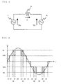
- Fig. 2 is a diagram showing a relation of operations among a source voltage, an input current, and switching means in the prior art.
- the first switching means 3 performs a one-pulse short-circuit operation with respect to half a cycle of the power source and the second switching means 4 is disposed for switching from a full-wave rectification to a voltage doubler rectification and vice versa.
- Fig. 2(a) shows a supply voltage waveform
- Fig. 2(b) an input current waveform
- Fig. 2(c) an operation waveform of the first switching means 3, respectively.
- a one-pulse short-circuit operation of with respect to half a cycle of the power source yields a spiked input current waveform like Fig. 2(b) .
- a current flows through the first switching means 3 by turning on the first switching means 3 for a predetermined time width Ton after an elapse of a predetermined delay time Tdl from a zero-cross point (a dark spot in Fig. 2 ) of the source voltage and a spiked current is added to yield the spiked input current.
- the second switching means 4 is disposed for the purpose of switching the full-wave rectification and the voltage doubler rectification, it can be configured by a mechanical switch such as a relay.
- the second switching means 4 enables the AC to DC converter to have two voltage reference levels of the output DC voltage applied to the DC load 8; the voltage by the full-wave rectification and the voltage by the voltage doubler rectification.
- the control range of the output voltage can be expanded.
- Fig. 3 is a circuit diagram equivalently showing operations of the AC to DC converter 100.
- the operation of the AC to DC converter 100 can be equivalently treated as if a virtual AC source 9 were connected in series with the reactor 5. That is, the first switching means 3 and the second switching means 4 operate so that the AC to DC converter 100 becomes equivalent to the virtual AC source 9.
- V s of the AC source 1 and the voltage V c of the virtual AC source 9 are supposed to be a sinusoidal shape and represented by (formula 2) and (formula 3) as follows.
- V s ⁇ ⁇ 2 ⁇ V 1 sin ⁇ t
- V c ⁇ ⁇ 2 ⁇ V 2 sin ⁇ t - ⁇
- circuit equation of Fig. 3 is represented using the voltage V c of the virtual AC source 9. From (formula 5), it can be said as follows.
- the first switching means 3 and the second switching means 4 are driven and controlled so that the voltage V c between the input terminals of the rectifier 2 becomes almost sinusoidal. Descriptions will be given to the operation of the first switching means 3 and the second switching means 4 to make the voltage V c to be almost sinusoidal.
- Fig. 4 is a diagram showing a waveform of an input terminal voltage Vc of a rectifier 2.
- the voltage Vc takes three levels of output conditions, voltage 0, V0/2, and V0 shown in Fig. 4 according to the operation of the first switching means 3 and the second switching means 4. It is the same with respect to a reverse polarity.
- V0 is an output DC voltage applied to the DC load 8. Operations of the first switching means 3 and the second switching means 4 will be explained by Fig. 5 in the following when taking output conditions of these three levels.
- Fig. 5 illustrates operations of the first switching means 3 and the second switching means 4. Each switching state of Fig. 5 will be explained as follows.
- the voltage Vc between the input terminals of the rectifier 2, that is the converter voltage Vc can take three-level voltage conditions.
- voltage waveforms such as intervals (1) to (3) in Fig. 4 can be generated and Vc can be output almost sinusoidally.
- Figs. 5(e) to 5(h) differ from Figs. 5(a) to 5(d) only in that the polarity of the AC source 1 is reversed.
- Figs. 5(e) to 5(h) correspond to intervals (1)' to (3)' in Fig. 4 .
- Embodiment 1 As mentioned above, operations of the first switching means 3 and the second switching means 4 to make the voltage Vc to be almost sinusoidal is explained. As explained above, in Embodiment 1, by making the output voltage level to be multi-stage (3 levels, 0, V0/2, and V0) compared with the prior art, the switching frequency is lowered and harmonic current is suppressed to enable the reactor 5 to be downsized.
- Embodiment 1 by driving and controlling the first switching means 3 and the second switching means 4 as explained in Figs. 4 and 5 , the voltage Vc between the input terminals of the rectifier 2, that is the converter voltage Vc, can be output almost sinusoidally.
- the reactor 5 can be downsized compared with a conventional technique, in which the switching means is made to operate once or several times for half a cycle of the voltage source.
- Embodiment 1 since the output voltage is made to be multi-leveled, it is possible to perform PWM control in which drive and control is performed at a low switching frequency of, for example, 1 kHz to 5kHz. Thereby, cost increase for noise reduction in such as performing high-frequency PWM control can be prevented. This is achieved because the input current can be almost sinusoidally controlled only by sinusoidally outputting the converter voltage Vc without controlling the input current. That is, high-frequency control operation becomes unnecessary because of no control of the input current.
- Embodiment 1 it is explained that by sinusoidally outputting the converter voltage Vc, the input voltage is made to be almost sinusoidal and harmonics can be suppressed.
- Embodiment 2 descriptions will be given to the control of the value of the output DC voltage V0 of the AC to DC converter 100. Circuit configuration of the AC to DC converter 100 is the same as Embodiment 1.
- Non Patent Literature 1 descriptions are given to a technique in which control is performed by obtaining an operation timing of the switching means in advance by calculation.
- An ON/OFF timing of the switching means can be set according to the phase angle without limit, therefore, innumerable candidates exist for solutions obtained by calculation. It was virtually difficult to obtain the ON/OFF timing for making the output DC voltage V0 to be a desired value under the above assumption.
- Non Patent Literature 1 a method is proposed in which using GA an optimal ON/OFF timing is searched in Non Patent Literature 1.
- no method has ever been found for searching the ON/OFF timing capable of making the output DC voltage V0 to be a desired value in addition to suppressing harmonics.
- a method of searching an optimal solution from infinitely existing ON/OFF timings is difficult to put into practice.
- the ON/OFF timing is determined by feedback control instead of obtaining the ON/OFF timing by calculation in advance.
- a method of determining the ON/OFF timing in Embodiment 2 will be explained.
- Fig. 6 is a diagram showing a vector relation of the circuit explained in Fig. 3 . Due to the affect of the reactor 5, the reactor current I becomes phase lag against the voltage Vs of the AC source 1. A voltage drop j ⁇ LI is generated in the reactor 5 so as to be orthogonal to the reactor current I. The result of vector addition of the voltage between the input terminals of the rectifier 2, which is the converter voltage Vc, with the voltage drop j ⁇ LI coincides with the voltage Vs of the AC source 1.
- the voltage Vs In order to output the converter voltage Vc so as to make power factor to be 1, the voltage Vs needs to be orthogonal to the voltage drop j ⁇ LI as shown in Fig. 6(b) . That is, the phase angle of the converter voltage Vc has only to be controlled so that a phase lag ⁇ against the AC source 1 of the converter voltage Vc becomes (formula 6) as follows.
- ⁇ tan - 1 ⁇ LI / V 1
- V2 of the converter voltage Vc has only to be output so as to be the value of (formula 7) as follows.
- V ⁇ 2 ⁇ ⁇ V 1 2 + ⁇ LI 2
- operation signals of the first switching means 3 and the second switching means 4 can be generated by applying such as saw-tooth wave modulation, triangular wave modulation, space vector modulation, and dipolar modulation.
- Fig. 7 is a control block diagram of the control means 20.
- a difference is input into a PI controller between a command value of the DC voltage and a detection value V0 of the DC voltage by a first voltage detector 21.
- the output of the PI controller is a current command value I*.
- the ON/OFF timing of the first switching means 3 and the second switching means 4 may be determined based on the phase angle ⁇ and the amplitude V2 obtained by the above procedure. Next, a method of coping with the change of the AC source 1 will be explained.
- the phase angle ⁇ is a function of the voltage Vs and the input current I of the AC source 1.
- the AC source 1 may be controlled with the value of V1 in the control block explained in Fig. 7 being the rated value.
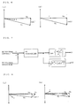
- Fig. 8 is a diagram showing variations of power factor through changes of the voltage of the AC source 1.
- the rated voltage of the AC source 1 is specified as Va.
- Fig. 8(a) shows a vector diagram when the voltage Vs becomes larger than the rated voltage Va
- Fig. 8(b) the vector diagram when the voltage Vs becomes smaller than the rated voltage Va.
- the amplitude V2 of the converter voltage Vc is subjected to voltage variations of the AC source 1 like the phase difference ⁇ , however, the voltage Vs of the AC source 1 has only to be detected.
- an effective value operation portion 23 calculates a voltage effective value of the AC source 1 based on a detection value of the second voltage detector 22 and control means 20 uses the calculation value for performing control.
- the effective value operation portion 23 detects the phase angle of the AC source 1 using a zero-cross point of the voltage of the AC source 1 detected by the second voltage detector 22.
- the control means 20 use the phase angle of the AC source 1 when controlling the phase angle of the converter voltage Vc. Then, in order to synchronize the phase angle ⁇ with the phase of the AC source 1, such as PLL (Phase Locked Loop) circuit may be employed. Thereby, it is possible to improve precision of the phase angle ⁇ to further reduce harmonics current.
- PLL Phase Locked Loop
- the converter voltage Vc can be decided.
- general unipolar modulation for example, can be employed as a method of deciding the ON/OFF timing of the first switching means 3 and the second switching means 4.
- Fig. 9 is a waveform diagram showing a modulation signal that specifies the ON/OFF timing of each switching means. Descriptions will be given to Fig. 9 as follows.
- Fig. 9(a) shows a modulation signal of the first switching means 3.
- Fig. 9(b) shows a modulation signal of the second switching means 4.
- Sinusoidal waveforms in Figs. 9(a) and 9(b) are the converter voltage Vc. since an absolute value of the negative electrode side corresponds to the value of the positive electrode side, the modular signal of the figure can be said to be a unipolar modulation method.
- Fig. 9(a) the first switching means 3 is turned off in the interval where the converter voltage Vc is larger than a triangle wave, which is a carrier wave.
- Fig. 9(c) is the ON/OFF timing of the first switching means 3. Hi-side is ON and Lo-side is OFF.
- the waveform of the modulation signal becomes Fig. 9(b) , which is 180-degree inverse of the phase of Fig. 9(a) .
- the waveform of Fig. 9(d) can be obtained, which is the ON/OFF timing of the second switching means 4.
- the converter voltage Vc can be obtained by summing waveforms of Figs. 9(c) and 9(d) .
- the Hi-side is ON of the switching means, therefore, addition is performed with Hi being 0 and Lo being 1 for the sake of simple explanation.
- the chopped converter voltage Vc of Fig. 9(e) can be obtained.
- two capacitors are connected in series, and under conditions of Figs. 5(b) and 5(c) , either of the capacitor is to be charged.
- the unipolar modulation explained in Fig. 9 the state in which only the first switching means 3 is ON and the state in which only the second switching means 4 is ON are alternatively generated. Therefore, the above problem can be avoided, and the unipolar modulation can be said to be a modulation method suitable for the present circuit configuration.
- Well-balanced distribution of the operation timing of the switching means may allow other modulation methods to be employed such as bipolar modulation, dipolar modulation, and saw-tooth wave modulation.
- the first diode 10 and the second diode 11 do not conduct and becomes an OFF state under a normal condition, in which the first capacitor 6 and the second capacitor 7 connected in parallel have charges to have a positive voltage, so that they are not connected virtually.
- the AC to DC converter 100 includes a first voltage detector 21 that detects the output DC voltage V0 and a second voltage detector 22 that detects the AC source voltage Vs to perform control based on these detected values. Thereby, even if the voltage of the AC source 1 changes, power factor improvement effect can be maintained.
- the AC to DC converter 100 according to Embodiment 2 can obtain a desired output DC voltage V0 by performing feedback control that performs feedback of detected values of the DC voltage to control command values.
- the AC to DC converter 100 according to Embodiment 2 can properly distribute operation timing of each switching means to almost sinusoidally output the converter voltage vc to suppress harmonic current using a modulation method such as unipolar modulation.
- Fig. 10 is a circuit diagram of the AC to DC converter 100 according to Embodiment 3.
- configuration of the switching means is changed from the circuit configuration in Fig. 1 .
- Other configurations are the same as Fig. 1 .
- IGBT 3a and 4a which are a unidirectional switching element, can perform an equivalent operation to the bidirectional switching means explained in Fig. 1 through a function of the diode rectifier 14. Accordingly, in the circuit configuration of Fig. 10 , the same control operation can be performed as those explained in Embodiments 1 and 2.
- Fig. 11 is a control block diagram of the control means 20 according to Embodiment 4.
- the control block (not shown) explained in Fig. 7 is connected with the left stage of Fig. 11 .
- a phase angle ⁇ and a amplitude V2 output by the control block of Fig. 7 are input. Operation of the control block of Fig. 11 will be explained as follows.
- the converter voltage Vc is output based on the voltage across the first capacitor 6 and the second capacitor 7.
- the rectifier 2 composed of semiconductors and each switching means are connected between input terminals of the rectifier 2 and across each capacitor.
- the amplitude V2 is corrected using the on-state voltage drop of the semiconductor and PWM control is performed using a value after the correction.
- error amount for the on-state voltage drop can be corrected.
- the voltage command value of the converter voltage can be obtained by calculating a ratio of the corrected voltage by the on-state voltage drop to the output DC voltage V0 to multiply it by the sin curve of the converter voltage Vc.
- the above control operation can be represented by the left-half control block of Fig. 11 .
- the current flows into each capacitor under the full-wave rectification state like Fig. 5(d) .
- a charging current flows through the first capacitor 6 and the second capacitor 7.
- the charging current becomes a large inrush current at the time of starting the AC to DC converter 100.
- the large current is considered to be the inrush current generated by a change in the rectification state from the full-wave rectification state into the voltage doubler rectification state when either the first switching means 3 or the second switching means 4 is turned on.
- a large inrush current at the time of starting the AC to DC converter 100 imposes a stress on every part of the AC to DC converter 100 such as each switching means and the rectifier 2. Therefore, it is desirable that the inrush current is suppressed as much as possible.
- Embodiment 4 the above-mentioned on-state voltage drop correction voltage will be employed. Descriptions will be given to a method of suppressing the inrush current using the on-state voltage drop correction voltage.
- the on-state voltage drop correction voltage becomes a positive value.
- the value is made to be negative, a higher voltage is output than the amplitude V2 obtained by the control block of Fig. 7 .
- each switching means is in OFF state. It is a state in which the current flows through the capacitor under the full-wave rectification state.
- the rate of the state of Figs. 5(d) and 5(h) is increased, and it is possible to reduce the rate, in which only one switching means becomes ON-state to become the voltage doubler state. Thereby, generation of the inrush current can be suppressed.
- the phase difference ⁇ between the converter voltage Vc and the voltage Vs of the AC source 1 is reset to be 0.
- the output DC voltage V0 is increased after the start-up.
- the phase difference ⁇ may be delayed. Therefore, control is performed such that the phase difference ⁇ is delayed after starting the AC to DC converter 100. Then, an abrupt increase in the output DC voltage may cause hunching of the control system in some cases.
- the phase difference ⁇ is set to be an advanced phase side (- 10 degree, for example) at the time of starting the AC to DC converter 100.
- the power source power factor can be improved (4 to 7 %, for example) more than the time without the correction.
- Embodiment 4 it is possible to increase the rate of the full-wave rectification state to suppress the generation of the inrush current by making the on-state voltage drop correction voltage to be a negative value when starting the AC to DC converter 100. After the start-up, by making the on-state voltage drop correction voltage to be a positive value as usual, while achieving a soft start-up, the above-mentioned power factor improvement effect can be demonstrated.
- Embodiment 4 it is possible to suppress an abrupt increase in the output DC voltage after the start-up because the phase difference ⁇ is made to be a negative value at the time of starting the AC to DC converter 100.
- Fig. 12 is a circuit diagram of the AC to DC converter 100 according to Embodiment 5.
- the circuit of Fig. 12 includes a current detector 24 and a zero-cross detector 25 in place of the second voltage detector 22 and the effective value operation portion 23 in the circuit configuration explained in Fig. 1 .
- the lowering of the power factor due to the voltage changes of the AC source 1 is coped with using detection results of the second voltage detector 22.
- the input current is detected using the current detector 24 instead thereof. Using the detection results, the power factor lowering is handled.
- the input current is detected using the current detector 24 to detect an instantaneous phase angle ⁇ (represented by ⁇ t in Embodiments 1 to 4) of the AC source 1.
- an instantaneous phase angle ⁇ represented by ⁇ t in Embodiments 1 to 4
- the voltage waveform of the AC source 1 is represented by a sin-function
- cos ⁇ from the phase angle to multiply it by the input current the reactive component of the AC source 1 can be obtained.
- the power factor 1.
- the phase difference ⁇ between the converter voltage Vc and the supply voltage Vs is too delayed, the reactive component of the input current becomes positive.
- the phase difference ⁇ is too much advanced, the reactive component of the input current becomes negative.
- the amplitude V2 is corrected only by the generation amount of the reactive current in the same way as the on-state voltage drop correction voltage explained in Embodiment 4. Thereby, feedback control becomes effective so that the phase of the input current becomes the same phase as that of the AC source 1 to prevent the power factor from being lowered.
- the lowering of the power factor may be detected, however, it is not possible to detect whether the phase is advanced or delayed. Therefore, it is not easily decided whether to make the correction voltage to be positive or negative.
- the reactive component of the current since a sign changes according to an advanced phase or a lagging phase, the polarity of the correction voltage can be easily obtained.
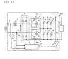
- Fig. 13 is a circuit diagram of the AC to DC converter 100 according to Embodiment 6. Being different from the circuit configuration of Embodiment 5, the circuit of Fig. 13 concurrently uses the second voltage detector 22 and the current detector 24. Thereby, even if a detection variation of, for example, about 5 to 10 % exists in either the second voltage detector 22 or the current detector 24, the lowering of the power factor can be suppressed by the control block to be explained in the following Fig. 14 .
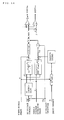
- Fig. 14 is a control block diagram of control means 20 according to Embodiment 6.
- Embodiment 6 when the supply voltage changes, the effective value of the supply voltage is detected, and at the same time, the reactive component of the input current is detected. These detected values are used for the control. Thereby, an affect of detection variations of the second voltage detector 22 and the current detector 24 is suppressed and a smooth start-up of the AC to DC converter 100 becomes possible.
- the control block diagram of Fig. 14 is configured such that the amplitude V2 is corrected in the same way as the on-state voltage drop correction voltage to make the reactive component of the input current to be 0, however, it may be configured to directly calculate the amplitude V2. In the latter case, it is only necessary to calculate the phase difference ⁇ from the reactive current to perform control of the output DC voltage using the amplitude V2.
- circuit configuration and the control block explained above perform feedback control so that the output DC voltage becomes a constant based on the principle explained in Fig. 3 .
- Other circuit configurations and control blocks may be used if they can perform feedback control of the output DC voltage based on a similar principle to improve the power factor and suppress the harmonics current even when changes of the power source voltages and detection variations of the detector exist.
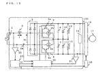
- Fig. 15 is a circuit diagram of the AC to DC converter 100 according to Embodiment 7.
- the DC load 8 in the circuit diagram explained in Fig. 13 is replaced by the inverter 18 and the permanent magnet motor 17. Further, a voltage clamp portion 19 is provided at the output end of the AC to DC converter 100. Moreover, an inverter control portion 26 is provided that controls the operation of the inverter 18.
- the inverter control portion 26 may be constituted by hardware such as a circuit device that achieves its function or may be configured by an operation device such as a microcomputer and CPU and software that specifies its operation.
- the “voltage increase suppression means” according to Embodiment 7 corresponds to the voltage clamp portion 19.
- the “motor deceleration means” corresponds to the control means 20, the inverter 18, and the inverter control portion 26.
- Embodiment 7 The operation of the AC to DC converter 100 according to Embodiment 7 is almost the same as those explained in Embodiments 1 to 6. Descriptions will be given to the replacement of the load by the inverter 18 and the permanent magnet motor 17 in particular. Firstly, it will be explained that using the circuit of Fig. 15 as a motor driver, degree of freedom in a motor design can be enhanced. Thereafter, descriptions will be given to a configuration that suppresses an instantaneous abnormal voltage increase, then an operation that safely drives the motor.
- a torque by a permanent magnet increases by making an induced voltage constant of the motor larger, therefore, the same torque can be output when the current is reduced.
- effects are demonstrated that reduce the conduction loss and switching loss of the inverter that drives the motor. Accordingly, to make the induced voltage constant of the motor larger to reduce the current is said to be the most effective for means of high efficiency.
- the output DC voltage V0 can be increased.
- the loss increases as much, exceeding the loss reduction effect of the AC to DC converter 100.
- control operation can be performed at a low carrier frequency, high efficiency conversion operation becomes possible by suppressing the lowering of the power factor while increasing the output voltage.
- the motor can be designed to have better efficiency at a low-speed operation and when operating the motor at high speed, the output DC voltage of the AC to DC converter 100 can be increased to secure the maximum rotation speed. Accordingly, it is possible to improve efficiency at low-speed driving, in other words, under normal use without lowering the performance of the air-conditioner even at the time of overload operation such as rapid cooling and rapid warming.
- the conventional control method like Fig. 2 may sometimes be suitable for use in place of the control in which three-level almost sinusoidal waves like Fig. 4 are output.
- the permanent magnet motor 17, the inverter 18, and the AC to DC converter 100 can be made to be totally high efficient by switching the method for controlling between the method of Fig.2 and that of Fig. 4 according to the rotation speed of the permanent magnet motor 17. Further, in the control method of Fig. 2 , pulse operation of several times can be performed for each half a cycle of the power supply. However, the number of the pulse is preferable that does not increase the amount of noise generation.
- the applied voltage may be detected, and control method may be switched between the method of Fig. 2 and that of Fig. 4 .
- a motor having a high induced voltage constant produces a large amount of power generation when performing free-running at high-speed rotation. This phenomenon becomes problematic at the time of stopping the permanent magnet motor 17.
- the AC to DC converter 100 according to the present invention is a regeneration type converter, therefore, no supplied energy can be consumed.
- the output DC voltage is made to increase, which is the voltage across both the first capacitor 6 and the second capacitor.
- the output DC voltage is made to increase, which is the voltage across both the first capacitor 6 and the second capacitor.
- the permanent magnet motor 17 sometimes steps out into stoppage due to such as poor torque. In this case, there is not much time to decelerate the permanent magnet motor 17, and some induced voltage constant of the permanent magnet motor 17 may cause the voltage exceeding withstand voltage of the first capacitor 6 and the second capacitor 7 to be applied to each capacitor.
- the AC to DC converter 100 according to Embodiment 7 is equipped with a voltage clamp portion 19 that suppresses an instantaneous abnormal voltage increase.
- the voltage clamp portion 19 may be constituted by a surge clamper, a surge absorber, or a series circuit of a resistor and an IGBT. Other configurations may be used that can suppress the instantaneous abnormal voltage increase.
- the AC to DC converter 100 When the voltage of the AC source 1 is lowered, the AC to DC converter 100 performs control such that the output DC voltage is made to be constant up to a control limit of the output DC voltage. However, the source voltage is lowered beyond the control limit, the output DC voltage cannot be increased, resulting in the lowering of the output DC voltage. If the permanent magnet motor 17 continues to rotate at the same rotation speed even when the output DC voltage is lowered, the permanent magnet motor 17 steps out into stoppage due to poor torque caused by poor DC voltage.
- the control means 20 commands the inverter control portion 2 6 to control the inverter 18 so as to decelerate the permanent magnet motor 17 when the second voltage detection means 22 detects the lowering of the source voltage. Then, regeneration energy by the deceleration of the permanent magnet motor 17 is regenerated into the first capacitor 6 and the second capacitor 7 to make the output DC voltage to increase. Thereby, necessary DC voltage can be secured and no step-out occurs in the permanent magnet motor 17. Moreover, a drop in the rotation speed of the permanent magnet motor 17 causes a decrease in the DC voltage value to be a limit to the step-out, therefore, the permanent magnet motor 17 hardly steps out into stoppage.
- a motor driving apparatus is configured that drives a motor having a high induced voltage constant using the AC to DC converter 100. Thereby, operation efficiency of the whole motor driving apparatus is improved and energy-saving effect can be improved.
- the voltage clamp portion 19 suppresses an instantaneous abnormal voltage increase to protect the first capacitor 6 and the second capacitor 7 from an excess voltage.
- the motor can be prevented from stepping out into stoppage because the motor is made to stop after deceleration.
- the motor is desirable to continue operation without stop as much as possible because stoppage of the motor causes an increase in the temperature in a freezer to increase the storage temperature when the motor is used in a freezer and the like.
- the second voltage detector 22 is used to detect a drop in the source voltage to make the AC to DC converter 100 and the inverter 18 to cooperatively operate, it is possible to provide a motor driver that is hard to stop even when instantaneous power failure occurs. It is also possible to provide a compressor driver that drives a compressor using the motor.
- the AC to DC converter 100 explained in Embodiments 1 to 7 can be utilized for a power unit for the load that consumes electric power in DC.
- the converter is applicable to home electronic appliances in general such as an air-conditioner, a freezing machine, a washing and drying machine, a refrigerator, a dehumidifier, a heat pump type water heater, a showcase, and a vacuum cleaner.
- it is applicable to a fan motor, a ventilator, and a hand drier, as well.
Landscapes
- Engineering & Computer Science (AREA)
- Power Engineering (AREA)
- Rectifiers (AREA)
- Control Of Ac Motors In General (AREA)
Applications Claiming Priority (1)
| Application Number | Priority Date | Filing Date | Title |
|---|---|---|---|
| PCT/JP2008/063835 WO2010013344A1 (ja) | 2008-08-01 | 2008-08-01 | 交流直流変換装置、交流直流変換装置の制御方法、電動機駆動装置、圧縮機駆動装置、空気調和機、ヒートポンプ式給湯機 |
Publications (3)
| Publication Number | Publication Date |
|---|---|
| EP2309635A1 true EP2309635A1 (de) | 2011-04-13 |
| EP2309635A4 EP2309635A4 (de) | 2013-07-03 |
| EP2309635B1 EP2309635B1 (de) | 2019-09-25 |
Family
ID=41610065
Family Applications (1)
| Application Number | Title | Priority Date | Filing Date |
|---|---|---|---|
| EP08792048.4A Active EP2309635B1 (de) | 2008-08-01 | 2008-08-01 | Wechselstrom-gleichstrom-wandler, wechselstrom-gleichstrom-wandlersteuerverfahren, motoransteuereinrichtung, kompressoransteuereinrichtung, klimaanlage und heisswasserversorgungseinrichtung des wärmepumpentyps |
Country Status (7)
| Country | Link |
|---|---|
| US (1) | US8508165B2 (de) |
| EP (1) | EP2309635B1 (de) |
| JP (1) | JP5355570B2 (de) |
| CN (1) | CN102106070B (de) |
| AU (1) | AU2008360120B2 (de) |
| ES (1) | ES2749875T3 (de) |
| WO (1) | WO2010013344A1 (de) |
Cited By (3)
| Publication number | Priority date | Publication date | Assignee | Title |
|---|---|---|---|---|
| EP2355329A4 (de) * | 2008-12-01 | 2013-05-01 | Mitsubishi Electric Corp | Wechselstrom-gleichstrom-wandlervorrichtung und vorrichtung zum ansteuern von elektrischen maschinen |
| WO2019088678A1 (en) | 2017-11-02 | 2019-05-09 | Samsung Electronics Co., Ltd. | Air conditioner and rectifier |
| EP3676945A4 (de) * | 2017-11-02 | 2020-11-04 | Samsung Electronics Co., Ltd. | Klimaanlage und gleichrichter |
Families Citing this family (51)
| Publication number | Priority date | Publication date | Assignee | Title |
|---|---|---|---|---|
| JP4254876B2 (ja) * | 2007-03-30 | 2009-04-15 | ダイキン工業株式会社 | 電源供給回路及びそのpam制御方法 |
| JP2011193593A (ja) * | 2010-03-12 | 2011-09-29 | Mitsubishi Electric Corp | 交流直流変換装置並びに空気調和機 |
| EP2555400A4 (de) * | 2010-03-29 | 2018-01-03 | Daikin Industries, Ltd. | Umschaltbare stromquellenschaltung |
| JP5079055B2 (ja) * | 2010-06-28 | 2012-11-21 | 三菱電機株式会社 | 電力変換装置 |
| JP2012044824A (ja) * | 2010-08-23 | 2012-03-01 | Fuji Electric Co Ltd | 電力変換装置 |
| JP5369073B2 (ja) * | 2010-10-08 | 2013-12-18 | 三菱電機株式会社 | 交流直流変換装置、交流直流変換装置を備えたモーター駆動装置、並びにモーター駆動装置を搭載した空気調和機、冷蔵庫、ヒートポンプ式給湯機、洗濯機及び掃除機 |
| JP2012191761A (ja) * | 2011-03-10 | 2012-10-04 | Fuji Electric Co Ltd | 交流−直流変換回路 |
| JP5222985B2 (ja) * | 2011-09-15 | 2013-06-26 | 株式会社安川電機 | 電源回生コンバータ、モータ駆動システム、及び電源回生処理方法 |
| US8796982B2 (en) * | 2011-12-15 | 2014-08-05 | Eaton Corporation | System and method for detecting phase loss and diagnosing DC link capacitor health in an adjustable speed drive |
| US20130322142A1 (en) * | 2012-05-31 | 2013-12-05 | General Electric Company | Multilevel power converter |
| KR101995864B1 (ko) * | 2012-07-25 | 2019-07-04 | 삼성전자주식회사 | 인버터 제어장치 및 그 제어방법 |
| EP2878074A1 (de) * | 2012-07-26 | 2015-06-03 | Osram Sylvania Inc. | Ac/dc-sperrwandler |
| CN103683468B (zh) * | 2012-09-17 | 2016-08-24 | 台达电子工业股份有限公司 | 电源系统以及电源系统的控制方法 |
| US9000707B2 (en) * | 2012-10-16 | 2015-04-07 | Toshiba International Corporation | Use of cooling fan in adjustable speed drives |
| WO2014086005A1 (zh) * | 2012-12-05 | 2014-06-12 | 中国北车股份有限公司大连电力牵引研发中心 | 整流牵引装置及内燃动车组 |
| BR102013003829A2 (pt) * | 2013-02-19 | 2014-11-04 | Whirlpool Sa | Método de acionamento de motor elétrico de lavadora |
| JP5825319B2 (ja) * | 2013-10-16 | 2015-12-02 | ダイキン工業株式会社 | 電力変換装置ならびに空気調和装置 |
| CN105829226B (zh) * | 2013-12-18 | 2020-04-14 | 奥的斯电梯公司 | 用于再生多电平驱动器的pwm策略 |
| US9982942B2 (en) | 2014-02-10 | 2018-05-29 | World Dryer Corporation | Dryer with universal voltage controller |
| WO2016051488A1 (ja) * | 2014-09-30 | 2016-04-07 | 三菱電機株式会社 | 電力変換装置 |
| KR102234374B1 (ko) * | 2015-02-19 | 2021-03-31 | 가부시키가이샤 에바라 세이사꾸쇼 | 드라이 진공 펌프 장치, 그 제어 방법 및 제어 프로그램 |
| JP6482994B2 (ja) * | 2015-09-08 | 2019-03-13 | 日立ジョンソンコントロールズ空調株式会社 | 電力変換装置および空気調和機 |
| JP6128201B1 (ja) * | 2015-12-28 | 2017-05-17 | ダイキン工業株式会社 | 電源装置、その電源装置を用いたインバータ装置、並びにコンバータ装置、及びそのインバータ装置又はコンバータ装置を用いた冷凍装置、並びに空気清浄器 |
| CN108575115B (zh) * | 2016-04-13 | 2022-04-05 | 株式会社日立产机系统 | 电动机系统 |
| US10312798B2 (en) | 2016-04-15 | 2019-06-04 | Emerson Electric Co. | Power factor correction circuits and methods including partial power factor correction operation for boost and buck power converters |
| US10763740B2 (en) | 2016-04-15 | 2020-09-01 | Emerson Climate Technologies, Inc. | Switch off time control systems and methods |
| US10277115B2 (en) | 2016-04-15 | 2019-04-30 | Emerson Climate Technologies, Inc. | Filtering systems and methods for voltage control |
| US10656026B2 (en) | 2016-04-15 | 2020-05-19 | Emerson Climate Technologies, Inc. | Temperature sensing circuit for transmitting data across isolation barrier |
| US10305373B2 (en) | 2016-04-15 | 2019-05-28 | Emerson Climate Technologies, Inc. | Input reference signal generation systems and methods |
| US9933842B2 (en) | 2016-04-15 | 2018-04-03 | Emerson Climate Technologies, Inc. | Microcontroller architecture for power factor correction converter |
| US10284132B2 (en) | 2016-04-15 | 2019-05-07 | Emerson Climate Technologies, Inc. | Driver for high-frequency switching voltage converters |
| JP6649622B2 (ja) * | 2016-05-24 | 2020-02-19 | サンケン電気株式会社 | コンデンサ放電回路 |
| US10498257B2 (en) * | 2016-06-30 | 2019-12-03 | Astec International Limited | Switching power converters controlled with control signals having variable on-times |
| WO2019049299A1 (ja) * | 2017-09-08 | 2019-03-14 | 三菱電機株式会社 | 電力変換装置、圧縮機、送風機、および空気調和装置 |
| CN109307835B (zh) * | 2018-03-12 | 2020-09-18 | 电子科技大学 | 基于锯齿波和遗传算法的模拟电路测点优选方法 |
| CN108469127A (zh) * | 2018-04-12 | 2018-08-31 | 合肥天鹅制冷科技有限公司 | 在双制式输入电源时统一制冷系统及方法 |
| WO2020031290A1 (ja) * | 2018-08-08 | 2020-02-13 | 三菱電機株式会社 | 負荷駆動装置、冷凍サイクル適用機器及び空気調和機 |
| CN112771775B (zh) * | 2018-09-28 | 2023-12-01 | 三菱电机株式会社 | 电力变换装置、马达驱动装置以及空气调节机 |
| WO2020095450A1 (ja) * | 2018-11-09 | 2020-05-14 | 株式会社安川電機 | 電力変換装置、圧送装置、及び制御方法 |
| KR102129927B1 (ko) * | 2018-12-21 | 2020-07-03 | 엘지전자 주식회사 | 공기조화기 |
| US11722086B2 (en) * | 2019-05-17 | 2023-08-08 | Mitsubishi Electric Corporation | Motor drive device |
| CN110203040B (zh) * | 2019-07-01 | 2024-01-12 | 合肥天鹅制冷科技有限公司 | 双制式双系统空调的控制系统 |
| CN114270688A (zh) * | 2019-08-30 | 2022-04-01 | 三菱电机株式会社 | 电力变换装置以及空气调节机 |
| CN110620413B (zh) * | 2019-10-14 | 2021-07-23 | 河北电立方新能源科技有限公司 | 电池系统的能量均衡电路 |
| JP2023521998A (ja) | 2020-04-13 | 2023-05-26 | エーイーエス グローバル ホールディングス, プライベート リミテッド | 電力回収を伴う入力インピーダンスネットワーク |
| CN111800001A (zh) * | 2020-04-28 | 2020-10-20 | 西安许继电力电子技术有限公司 | 一种直流变压器串联侧母线电容均压装置及均压方法 |
| US11711022B2 (en) * | 2021-04-13 | 2023-07-25 | Advanced Energy Industries, Inc. | Series stack switch circuit with voltage clamping and power recovery |
| US11705822B2 (en) * | 2021-04-13 | 2023-07-18 | Advanced Energy Industries, Inc. | Voltage clamp and current clamp systems with power recovery |
| CN113067470B (zh) * | 2021-06-02 | 2021-08-17 | 上海芯龙半导体技术股份有限公司 | 用于开关电源芯片的使能电路、开关电源芯片及控制方法 |
| KR20240045279A (ko) * | 2021-08-11 | 2024-04-05 | 램 리써치 코포레이션 | 히터 온도를 제어하기 위해 정류기 및 벅 스테이지 (buck stage) 를 사용하는 전압의 진폭 변조 |
| CN114019283B (zh) * | 2021-11-04 | 2024-06-21 | 杭州老板电器股份有限公司 | 电容故障检测方法、装置及油烟机 |
Family Cites Families (22)
| Publication number | Priority date | Publication date | Assignee | Title |
|---|---|---|---|---|
| CA1053791A (en) * | 1975-08-21 | 1979-05-01 | General Signal Corporation | Vital relay operating circuit |
| JPH0789743B2 (ja) | 1983-04-26 | 1995-09-27 | 株式会社東芝 | 整流電源回路 |
| JPS61224866A (ja) * | 1985-03-29 | 1986-10-06 | Toshiba Corp | 電力変換装置の制御装置 |
| JP2763479B2 (ja) | 1992-08-06 | 1998-06-11 | 三菱電機株式会社 | 直流電源装置 |
| JP3527531B2 (ja) * | 1993-06-15 | 2004-05-17 | ローム株式会社 | パッケージ型固体電解コンデンサ |
| JP3422218B2 (ja) * | 1996-10-11 | 2003-06-30 | ダイキン工業株式会社 | コンバータ |
| JPH10191640A (ja) * | 1996-12-26 | 1998-07-21 | Hitachi Ltd | コンバータの制御装置 |
| TW528847B (en) * | 1998-06-18 | 2003-04-21 | Hitachi Ltd | Refrigerator |
| CN1183654C (zh) * | 1999-01-19 | 2005-01-05 | 松下电器产业株式会社 | 电源装置及使用了该电源的空调机 |
| JP2001145360A (ja) * | 1999-11-16 | 2001-05-25 | Hitachi Ltd | 力率改善回路,モータ制御装置及び空調機 |
| JP3485047B2 (ja) | 1999-11-24 | 2004-01-13 | 三菱電機株式会社 | 空気調和機 |
| JP3934982B2 (ja) | 2001-04-17 | 2007-06-20 | 松下電器産業株式会社 | 電源装置 |
| JP3687641B2 (ja) | 2002-10-01 | 2005-08-24 | 松下電器産業株式会社 | インバ−タエアコン |
| US6984948B2 (en) * | 2002-12-12 | 2006-01-10 | Matsushita Electric Industrial Co., Ltd. | Motor control apparatus |
| JP2004229462A (ja) * | 2003-01-27 | 2004-08-12 | Rohm Co Ltd | 電動機の制御装置 |
| KR100654487B1 (ko) * | 2003-09-09 | 2006-12-05 | 마츠시타 덴끼 산교 가부시키가이샤 | 컨버터 회로, 모터 구동 장치, 압축기, 공기 조화기,냉장고, 전기 세탁기, 송풍기, 전기 청소기 및 히트펌프급탕기 |
| JP2005094982A (ja) * | 2003-09-19 | 2005-04-07 | Toshiba Corp | モータの駆動装置 |
| CN1753294A (zh) * | 2004-09-22 | 2006-03-29 | 松下电器产业株式会社 | 直流电源装置、控制方法以及压缩机驱动装置 |
| JP2007110779A (ja) * | 2005-10-11 | 2007-04-26 | Matsushita Electric Ind Co Ltd | モータ駆動装置および駆動方法 |
| JP2008022625A (ja) | 2006-07-12 | 2008-01-31 | Fuji Electric Systems Co Ltd | 交流−直流変換装置 |
| JP2008099512A (ja) * | 2006-10-16 | 2008-04-24 | Matsushita Electric Ind Co Ltd | 電源装置 |
| JP5230182B2 (ja) | 2006-12-13 | 2013-07-10 | キヤノン株式会社 | スイッチング電源装置 |
-
2008
- 2008-08-01 WO PCT/JP2008/063835 patent/WO2010013344A1/ja not_active Ceased
- 2008-08-01 ES ES08792048T patent/ES2749875T3/es active Active
- 2008-08-01 EP EP08792048.4A patent/EP2309635B1/de active Active
- 2008-08-01 AU AU2008360120A patent/AU2008360120B2/en not_active Ceased
- 2008-08-01 US US13/002,221 patent/US8508165B2/en active Active
- 2008-08-01 CN CN200880130527.9A patent/CN102106070B/zh not_active Expired - Fee Related
- 2008-08-01 JP JP2010522573A patent/JP5355570B2/ja active Active
Cited By (5)
| Publication number | Priority date | Publication date | Assignee | Title |
|---|---|---|---|---|
| EP2355329A4 (de) * | 2008-12-01 | 2013-05-01 | Mitsubishi Electric Corp | Wechselstrom-gleichstrom-wandlervorrichtung und vorrichtung zum ansteuern von elektrischen maschinen |
| US8823303B2 (en) | 2008-12-01 | 2014-09-02 | Mitsubishi Electric Corporation | Alternating-current direct-current converter and electric motor driver |
| WO2019088678A1 (en) | 2017-11-02 | 2019-05-09 | Samsung Electronics Co., Ltd. | Air conditioner and rectifier |
| US10734910B2 (en) | 2017-11-02 | 2020-08-04 | Samsung Electronics Co., Ltd. | Air conditioner and rectifier |
| EP3676945A4 (de) * | 2017-11-02 | 2020-11-04 | Samsung Electronics Co., Ltd. | Klimaanlage und gleichrichter |
Also Published As
| Publication number | Publication date |
|---|---|
| CN102106070A (zh) | 2011-06-22 |
| ES2749875T3 (es) | 2020-03-24 |
| EP2309635A4 (de) | 2013-07-03 |
| JP5355570B2 (ja) | 2013-11-27 |
| AU2008360120B2 (en) | 2013-10-31 |
| AU2008360120A1 (en) | 2010-02-04 |
| CN102106070B (zh) | 2014-03-05 |
| WO2010013344A1 (ja) | 2010-02-04 |
| US20110101898A1 (en) | 2011-05-05 |
| US8508165B2 (en) | 2013-08-13 |
| EP2309635B1 (de) | 2019-09-25 |
| JPWO2010013344A1 (ja) | 2012-01-05 |
Similar Documents
| Publication | Publication Date | Title |
|---|---|---|
| EP2309635B1 (de) | Wechselstrom-gleichstrom-wandler, wechselstrom-gleichstrom-wandlersteuerverfahren, motoransteuereinrichtung, kompressoransteuereinrichtung, klimaanlage und heisswasserversorgungseinrichtung des wärmepumpentyps | |
| US8823303B2 (en) | Alternating-current direct-current converter and electric motor driver | |
| JP5769764B2 (ja) | 交流直流変換装置、電動機駆動装置、圧縮機駆動装置、空気調和機、ヒートポンプ式給湯機 | |
| EP2184842B1 (de) | Wechselstrom-/gleichstrom-wandler und kompressorantriebseinheit und diese verwendende klimaanlage | |
| CN109937531B (zh) | 电力转换装置及冷冻空调机器 | |
| JP7554301B2 (ja) | 運転制御方法、回路、家電機器及びコンピュータ読み取り可能な記憶媒体 | |
| KR20160065618A (ko) | 모터 구동 장치, 이를 포함하는 공기조화기 및 그의 제어방법 | |
| CN103098362B (zh) | 电力变换装置、电动机驱动设备、制冷空调设备 | |
| JP6596323B2 (ja) | コンバータ装置、駆動制御装置、モータ、およびコンプレッサ | |
| CN107567680A (zh) | 具有有源转换器的变速驱动器 | |
| US20170153051A1 (en) | Direct-current power supply device and refrigeration-cycle applied device including the same | |
| JP2018007327A (ja) | 直流電源装置および空気調和機 | |
| KR102043950B1 (ko) | 전력변환장치 및 이를 포함하는 공기조화기 | |
| CN107707104B (zh) | 无滤波电容的三相变频器及其控制方法 | |
| KR20110077801A (ko) | 직류전원 공급장치 및 직류전원 공급방법 | |
| CN108450057B (zh) | 功率转换装置的控制装置 | |
| JP6695028B2 (ja) | 整流回路装置 | |
| JP2015091186A (ja) | モータインバータ装置 | |
| WO2019163068A1 (ja) | 整流回路装置 | |
| JP6156100B2 (ja) | 電源装置及びこれを搭載した空気調和機 |
Legal Events
| Date | Code | Title | Description |
|---|---|---|---|
| PUAI | Public reference made under article 153(3) epc to a published international application that has entered the european phase |
Free format text: ORIGINAL CODE: 0009012 |
|
| 17P | Request for examination filed |
Effective date: 20110111 |
|
| AK | Designated contracting states |
Kind code of ref document: A1 Designated state(s): AT BE BG CH CY CZ DE DK EE ES FI FR GB GR HR HU IE IS IT LI LT LU LV MC MT NL NO PL PT RO SE SI SK TR |
|
| AX | Request for extension of the european patent |
Extension state: AL BA MK RS |
|
| DAX | Request for extension of the european patent (deleted) | ||
| A4 | Supplementary search report drawn up and despatched |
Effective date: 20130605 |
|
| RIC1 | Information provided on ipc code assigned before grant |
Ipc: H02M 1/12 20060101AFI20130530BHEP Ipc: H02M 1/36 20070101ALI20130530BHEP Ipc: H02M 1/42 20070101ALI20130530BHEP |
|
| 17Q | First examination report despatched |
Effective date: 20161006 |
|
| STAA | Information on the status of an ep patent application or granted ep patent |
Free format text: STATUS: EXAMINATION IS IN PROGRESS |
|
| GRAP | Despatch of communication of intention to grant a patent |
Free format text: ORIGINAL CODE: EPIDOSNIGR1 |
|
| STAA | Information on the status of an ep patent application or granted ep patent |
Free format text: STATUS: GRANT OF PATENT IS INTENDED |
|
| INTG | Intention to grant announced |
Effective date: 20190319 |
|
| GRAS | Grant fee paid |
Free format text: ORIGINAL CODE: EPIDOSNIGR3 |
|
| GRAA | (expected) grant |
Free format text: ORIGINAL CODE: 0009210 |
|
| STAA | Information on the status of an ep patent application or granted ep patent |
Free format text: STATUS: THE PATENT HAS BEEN GRANTED |
|
| AK | Designated contracting states |
Kind code of ref document: B1 Designated state(s): AT BE BG CH CY CZ DE DK EE ES FI FR GB GR HR HU IE IS IT LI LT LU LV MC MT NL NO PL PT RO SE SI SK TR |
|
| REG | Reference to a national code |
Ref country code: GB Ref legal event code: FG4D |
|
| REG | Reference to a national code |
Ref country code: CH Ref legal event code: EP |
|
| REG | Reference to a national code |
Ref country code: AT Ref legal event code: REF Ref document number: 1184785 Country of ref document: AT Kind code of ref document: T Effective date: 20191015 |
|
| REG | Reference to a national code |
Ref country code: IE Ref legal event code: FG4D |
|
| REG | Reference to a national code |
Ref country code: DE Ref legal event code: R096 Ref document number: 602008061286 Country of ref document: DE |
|
| REG | Reference to a national code |
Ref country code: NL Ref legal event code: MP Effective date: 20190925 |
|
| PG25 | Lapsed in a contracting state [announced via postgrant information from national office to epo] |
Ref country code: NO Free format text: LAPSE BECAUSE OF FAILURE TO SUBMIT A TRANSLATION OF THE DESCRIPTION OR TO PAY THE FEE WITHIN THE PRESCRIBED TIME-LIMIT Effective date: 20191225 Ref country code: BG Free format text: LAPSE BECAUSE OF FAILURE TO SUBMIT A TRANSLATION OF THE DESCRIPTION OR TO PAY THE FEE WITHIN THE PRESCRIBED TIME-LIMIT Effective date: 20191225 Ref country code: SE Free format text: LAPSE BECAUSE OF FAILURE TO SUBMIT A TRANSLATION OF THE DESCRIPTION OR TO PAY THE FEE WITHIN THE PRESCRIBED TIME-LIMIT Effective date: 20190925 Ref country code: FI Free format text: LAPSE BECAUSE OF FAILURE TO SUBMIT A TRANSLATION OF THE DESCRIPTION OR TO PAY THE FEE WITHIN THE PRESCRIBED TIME-LIMIT Effective date: 20190925 Ref country code: LT Free format text: LAPSE BECAUSE OF FAILURE TO SUBMIT A TRANSLATION OF THE DESCRIPTION OR TO PAY THE FEE WITHIN THE PRESCRIBED TIME-LIMIT Effective date: 20190925 Ref country code: HR Free format text: LAPSE BECAUSE OF FAILURE TO SUBMIT A TRANSLATION OF THE DESCRIPTION OR TO PAY THE FEE WITHIN THE PRESCRIBED TIME-LIMIT Effective date: 20190925 |
|
| REG | Reference to a national code |
Ref country code: LT Ref legal event code: MG4D |
|
| PG25 | Lapsed in a contracting state [announced via postgrant information from national office to epo] |
Ref country code: GR Free format text: LAPSE BECAUSE OF FAILURE TO SUBMIT A TRANSLATION OF THE DESCRIPTION OR TO PAY THE FEE WITHIN THE PRESCRIBED TIME-LIMIT Effective date: 20191226 Ref country code: LV Free format text: LAPSE BECAUSE OF FAILURE TO SUBMIT A TRANSLATION OF THE DESCRIPTION OR TO PAY THE FEE WITHIN THE PRESCRIBED TIME-LIMIT Effective date: 20190925 |
|
| REG | Reference to a national code |
Ref country code: ES Ref legal event code: FG2A Ref document number: 2749875 Country of ref document: ES Kind code of ref document: T3 Effective date: 20200324 |
|
| REG | Reference to a national code |
Ref country code: AT Ref legal event code: MK05 Ref document number: 1184785 Country of ref document: AT Kind code of ref document: T Effective date: 20190925 |
|
| PG25 | Lapsed in a contracting state [announced via postgrant information from national office to epo] |
Ref country code: AT Free format text: LAPSE BECAUSE OF FAILURE TO SUBMIT A TRANSLATION OF THE DESCRIPTION OR TO PAY THE FEE WITHIN THE PRESCRIBED TIME-LIMIT Effective date: 20190925 Ref country code: PT Free format text: LAPSE BECAUSE OF FAILURE TO SUBMIT A TRANSLATION OF THE DESCRIPTION OR TO PAY THE FEE WITHIN THE PRESCRIBED TIME-LIMIT Effective date: 20200127 Ref country code: EE Free format text: LAPSE BECAUSE OF FAILURE TO SUBMIT A TRANSLATION OF THE DESCRIPTION OR TO PAY THE FEE WITHIN THE PRESCRIBED TIME-LIMIT Effective date: 20190925 Ref country code: PL Free format text: LAPSE BECAUSE OF FAILURE TO SUBMIT A TRANSLATION OF THE DESCRIPTION OR TO PAY THE FEE WITHIN THE PRESCRIBED TIME-LIMIT Effective date: 20190925 Ref country code: RO Free format text: LAPSE BECAUSE OF FAILURE TO SUBMIT A TRANSLATION OF THE DESCRIPTION OR TO PAY THE FEE WITHIN THE PRESCRIBED TIME-LIMIT Effective date: 20190925 Ref country code: NL Free format text: LAPSE BECAUSE OF FAILURE TO SUBMIT A TRANSLATION OF THE DESCRIPTION OR TO PAY THE FEE WITHIN THE PRESCRIBED TIME-LIMIT Effective date: 20190925 |
|
| PG25 | Lapsed in a contracting state [announced via postgrant information from national office to epo] |
Ref country code: CZ Free format text: LAPSE BECAUSE OF FAILURE TO SUBMIT A TRANSLATION OF THE DESCRIPTION OR TO PAY THE FEE WITHIN THE PRESCRIBED TIME-LIMIT Effective date: 20190925 Ref country code: SK Free format text: LAPSE BECAUSE OF FAILURE TO SUBMIT A TRANSLATION OF THE DESCRIPTION OR TO PAY THE FEE WITHIN THE PRESCRIBED TIME-LIMIT Effective date: 20190925 Ref country code: IS Free format text: LAPSE BECAUSE OF FAILURE TO SUBMIT A TRANSLATION OF THE DESCRIPTION OR TO PAY THE FEE WITHIN THE PRESCRIBED TIME-LIMIT Effective date: 20200224 |
|
| REG | Reference to a national code |
Ref country code: DE Ref legal event code: R097 Ref document number: 602008061286 Country of ref document: DE |
|
| PG2D | Information on lapse in contracting state deleted |
Ref country code: IS |
|
| PG25 | Lapsed in a contracting state [announced via postgrant information from national office to epo] |
Ref country code: DK Free format text: LAPSE BECAUSE OF FAILURE TO SUBMIT A TRANSLATION OF THE DESCRIPTION OR TO PAY THE FEE WITHIN THE PRESCRIBED TIME-LIMIT Effective date: 20190925 Ref country code: IS Free format text: LAPSE BECAUSE OF FAILURE TO SUBMIT A TRANSLATION OF THE DESCRIPTION OR TO PAY THE FEE WITHIN THE PRESCRIBED TIME-LIMIT Effective date: 20200126 |
|
| PLBE | No opposition filed within time limit |
Free format text: ORIGINAL CODE: 0009261 |
|
| STAA | Information on the status of an ep patent application or granted ep patent |
Free format text: STATUS: NO OPPOSITION FILED WITHIN TIME LIMIT |
|
| 26N | No opposition filed |
Effective date: 20200626 |
|
| PG25 | Lapsed in a contracting state [announced via postgrant information from national office to epo] |
Ref country code: SI Free format text: LAPSE BECAUSE OF FAILURE TO SUBMIT A TRANSLATION OF THE DESCRIPTION OR TO PAY THE FEE WITHIN THE PRESCRIBED TIME-LIMIT Effective date: 20190925 |
|
| PG25 | Lapsed in a contracting state [announced via postgrant information from national office to epo] |
Ref country code: MC Free format text: LAPSE BECAUSE OF FAILURE TO SUBMIT A TRANSLATION OF THE DESCRIPTION OR TO PAY THE FEE WITHIN THE PRESCRIBED TIME-LIMIT Effective date: 20190925 |
|
| REG | Reference to a national code |
Ref country code: CH Ref legal event code: PL |
|
| GBPC | Gb: european patent ceased through non-payment of renewal fee |
Effective date: 20200801 |
|
| PG25 | Lapsed in a contracting state [announced via postgrant information from national office to epo] |
Ref country code: LU Free format text: LAPSE BECAUSE OF NON-PAYMENT OF DUE FEES Effective date: 20200801 Ref country code: LI Free format text: LAPSE BECAUSE OF NON-PAYMENT OF DUE FEES Effective date: 20200831 Ref country code: CH Free format text: LAPSE BECAUSE OF NON-PAYMENT OF DUE FEES Effective date: 20200831 |
|
| REG | Reference to a national code |
Ref country code: BE Ref legal event code: MM Effective date: 20200831 |
|
| PG25 | Lapsed in a contracting state [announced via postgrant information from national office to epo] |
Ref country code: IE Free format text: LAPSE BECAUSE OF NON-PAYMENT OF DUE FEES Effective date: 20200801 Ref country code: GB Free format text: LAPSE BECAUSE OF NON-PAYMENT OF DUE FEES Effective date: 20200801 Ref country code: BE Free format text: LAPSE BECAUSE OF NON-PAYMENT OF DUE FEES Effective date: 20200831 |
|
| PG25 | Lapsed in a contracting state [announced via postgrant information from national office to epo] |
Ref country code: TR Free format text: LAPSE BECAUSE OF FAILURE TO SUBMIT A TRANSLATION OF THE DESCRIPTION OR TO PAY THE FEE WITHIN THE PRESCRIBED TIME-LIMIT Effective date: 20190925 Ref country code: MT Free format text: LAPSE BECAUSE OF FAILURE TO SUBMIT A TRANSLATION OF THE DESCRIPTION OR TO PAY THE FEE WITHIN THE PRESCRIBED TIME-LIMIT Effective date: 20190925 Ref country code: CY Free format text: LAPSE BECAUSE OF FAILURE TO SUBMIT A TRANSLATION OF THE DESCRIPTION OR TO PAY THE FEE WITHIN THE PRESCRIBED TIME-LIMIT Effective date: 20190925 |
|
| REG | Reference to a national code |
Ref country code: DE Ref legal event code: R084 Ref document number: 602008061286 Country of ref document: DE |
|
| P01 | Opt-out of the competence of the unified patent court (upc) registered |
Effective date: 20230512 |
|
| PGFP | Annual fee paid to national office [announced via postgrant information from national office to epo] |
Ref country code: IT Payment date: 20230711 Year of fee payment: 16 Ref country code: ES Payment date: 20230901 Year of fee payment: 16 |
|
| PGFP | Annual fee paid to national office [announced via postgrant information from national office to epo] |
Ref country code: FR Payment date: 20230703 Year of fee payment: 16 Ref country code: DE Payment date: 20230627 Year of fee payment: 16 |
|
| REG | Reference to a national code |
Ref country code: ES Ref legal event code: GC2A Effective date: 20231215 |
|
| REG | Reference to a national code |
Ref country code: DE Ref legal event code: R119 Ref document number: 602008061286 Country of ref document: DE |
|
| PG25 | Lapsed in a contracting state [announced via postgrant information from national office to epo] |
Ref country code: DE Free format text: LAPSE BECAUSE OF NON-PAYMENT OF DUE FEES Effective date: 20250301 |
|
| PG25 | Lapsed in a contracting state [announced via postgrant information from national office to epo] |
Ref country code: IT Free format text: LAPSE BECAUSE OF NON-PAYMENT OF DUE FEES Effective date: 20240801 |
|
| PG25 | Lapsed in a contracting state [announced via postgrant information from national office to epo] |
Ref country code: FR Free format text: LAPSE BECAUSE OF NON-PAYMENT OF DUE FEES Effective date: 20240831 |
|
| REG | Reference to a national code |
Ref country code: ES Ref legal event code: FD2A Effective date: 20250926 |
|
| PG25 | Lapsed in a contracting state [announced via postgrant information from national office to epo] |
Ref country code: ES Free format text: LAPSE BECAUSE OF NON-PAYMENT OF DUE FEES Effective date: 20240802 |