EP2311092B1 - Capteur d'images à champ lumineux, procédé et applications - Google Patents
Capteur d'images à champ lumineux, procédé et applications Download PDFInfo
- Publication number
- EP2311092B1 EP2311092B1 EP09820950.5A EP09820950A EP2311092B1 EP 2311092 B1 EP2311092 B1 EP 2311092B1 EP 09820950 A EP09820950 A EP 09820950A EP 2311092 B1 EP2311092 B1 EP 2311092B1
- Authority
- EP
- European Patent Office
- Prior art keywords
- light
- periodic
- grating
- gratings
- diodes
- Prior art date
- Legal status (The legal status is an assumption and is not a legal conclusion. Google has not performed a legal analysis and makes no representation as to the accuracy of the status listed.)
- Active
Links
Images









Classifications
-
- G—PHYSICS
- G01—MEASURING; TESTING
- G01B—MEASURING LENGTH, THICKNESS OR SIMILAR LINEAR DIMENSIONS; MEASURING ANGLES; MEASURING AREAS; MEASURING IRREGULARITIES OF SURFACES OR CONTOURS
- G01B11/00—Measuring arrangements characterised by the use of optical techniques
- G01B11/14—Measuring arrangements characterised by the use of optical techniques for measuring distance or clearance between spaced objects or spaced apertures
-
- G—PHYSICS
- G01—MEASURING; TESTING
- G01S—RADIO DIRECTION-FINDING; RADIO NAVIGATION; DETERMINING DISTANCE OR VELOCITY BY USE OF RADIO WAVES; LOCATING OR PRESENCE-DETECTING BY USE OF THE REFLECTION OR RERADIATION OF RADIO WAVES; ANALOGOUS ARRANGEMENTS USING OTHER WAVES
- G01S3/00—Direction-finders for determining the direction from which infrasonic, sonic, ultrasonic or electromagnetic waves, or particle emission, not having a directional significance, are being received
- G01S3/78—Direction-finders for determining the direction from which infrasonic, sonic, ultrasonic or electromagnetic waves, or particle emission, not having a directional significance, are being received using electromagnetic waves other than radio waves
- G01S3/782—Systems for determining direction or deviation from predetermined direction
-
- H—ELECTRICITY
- H10—SEMICONDUCTOR DEVICES; ELECTRIC SOLID-STATE DEVICES NOT OTHERWISE PROVIDED FOR
- H10F—INORGANIC SEMICONDUCTOR DEVICES SENSITIVE TO INFRARED RADIATION, LIGHT, ELECTROMAGNETIC RADIATION OF SHORTER WAVELENGTH OR CORPUSCULAR RADIATION
- H10F39/00—Integrated devices, or assemblies of multiple devices, comprising at least one element covered by group H10F30/00, e.g. radiation detectors comprising photodiode arrays
- H10F39/10—Integrated devices
- H10F39/12—Image sensors
-
- G—PHYSICS
- G01—MEASURING; TESTING
- G01N—INVESTIGATING OR ANALYSING MATERIALS BY DETERMINING THEIR CHEMICAL OR PHYSICAL PROPERTIES
- G01N21/00—Investigating or analysing materials by the use of optical means, i.e. using sub-millimetre waves, infrared, visible or ultraviolet light
- G01N21/62—Systems in which the material investigated is excited whereby it emits light or causes a change in wavelength of the incident light
- G01N21/63—Systems in which the material investigated is excited whereby it emits light or causes a change in wavelength of the incident light optically excited
- G01N21/64—Fluorescence; Phosphorescence
-
- H—ELECTRICITY
- H10—SEMICONDUCTOR DEVICES; ELECTRIC SOLID-STATE DEVICES NOT OTHERWISE PROVIDED FOR
- H10F—INORGANIC SEMICONDUCTOR DEVICES SENSITIVE TO INFRARED RADIATION, LIGHT, ELECTROMAGNETIC RADIATION OF SHORTER WAVELENGTH OR CORPUSCULAR RADIATION
- H10F39/00—Integrated devices, or assemblies of multiple devices, comprising at least one element covered by group H10F30/00, e.g. radiation detectors comprising photodiode arrays
- H10F39/10—Integrated devices
- H10F39/107—Integrated devices having multiple elements covered by H10F30/00 in a repetitive configuration, e.g. radiation detectors comprising photodiode arrays
-
- G—PHYSICS
- G01—MEASURING; TESTING
- G01N—INVESTIGATING OR ANALYSING MATERIALS BY DETERMINING THEIR CHEMICAL OR PHYSICAL PROPERTIES
- G01N2201/00—Features of devices classified in G01N21/00
- G01N2201/06—Illumination; Optics
- G01N2201/062—LED's
Definitions
- Embodiments of the invention are directed to a lens-less, angle-sensitive pixel (ASP) device and to a lens-less light field image detector for measuring the intensity and direction angle of a light field to provide an image of the light field.
- ASP angle-sensitive pixel
- Pixel-scale angle-sensitive structures have been demonstrated on chip but require post-assembled arrays of microlenses, which significantly increase cost and complexity over the manufacture and use of standard imagers.
- SOI silicon-on-insulator
- Document EP 1 731 099 A1 discloses an x-ray interferometer arrangement comprising a beam splitter grating and an analyser grating.
- the distance between beam splitter and analyzer is chosen to be an odd fractional Talbot distance.
- Document US 2005/0286680 A1 discloses an X-ray imaging apparatus equipped with first and second diffraction gratings and an X-ray image detector.
- the first diffraction grating is constructed to generate the Talbot effect using X-rays irradiated at the first diffraction grating.
- the second diffraction grating is configured so as to diffract the X-rays diffracted by the first diffraction grating.
- the X-ray image detector is configured so as to detect the X-rays diffracted by the second diffraction grating.
- Document WO 2007/125833 A1 discloses an X-ray imaging apparatus and image picking-up method based on the principle of Talbot interferometer.
- Document US 2006/044429 A1 discloses an imaging apparatus provided with a wavelength dispersion unit that divides the electromagnetic waves into wavelength components by diffraction such that divided components are distributed on the electromagnetic wave incident surface of device.
- the wavelength dispersion unit comprises a first diffraction grating and a second diffraction grating generating interference fringes, signals are detected for different wavelengths by respective photoelectric conversion elements in a photodiode group.
- CMOS complementary metal-oxide-semiconductor
- the present invention is set out in the independent claim, with optional features set out in the dependent claim.
- An embodiment of the invention is a lens-less, angle-sensitive pixel (ASP) device as defined in claim 1.
- the first and second pixel devices further comprise a first intermediate periodic, light diffracting structure having a period, p 1 , disposed between the first periodic, light diffracting structure and the second periodic structure, oriented perpendicularly to the first and second periodic structures; and a second intermediate periodic, light diffracting structure having a period, p 2 , disposed between the second periodic structure and the first and second sensors, oriented perpendicularly to the first and second periodic structures, wherein in the first pixel device, the first and second intermediate periodic, light diffracting structures are not laterally displaced from the respective first and second periodic structure, further wherein in the second pixel device, the first and second intermediate periodic, light diffracting structures are laterally displaced from the respective first and second periodic structures by an amount ( m 2 / n 2 )p 1 .
- the detector further comprises at least an n th (n ⁇ 3) pixel device disposed linearly adjacent the (n th - 1) pixel device, including a first periodic, light diffracting structure having a period, p 1 , disposed in or on a top surface of the support structure; a second periodic structure having a period, p 2 , oriented parallel to the first periodic, light diffracting structure and disposed in the support structure at the selected distance below the first periodic, light diffracting structure, wherein the second periodic structure is laterally displaced from the first periodic, light diffracting structure by an amount ( m n / n )p 1 , where ( m n / n n ) > ( m n-1 / n n-1 ) ; and an n th sensor disposed in the support structure at the first selected distance below the first periodic, light diffracting structure.
- every n th (n ⁇ 3) pixel device further comprises a first intermediate periodic, light diffracting structure having a period, p 1 , disposed between the first periodic structure and the second periodic structure, oriented perpendicularly to the first and second periodic structures; and a second intermediate periodic, light diffracting structure having a period, p 2 , disposed between the second periodic structure and the n th sensors, oriented perpendicularly to the first and second periodic structures, wherein in every n th (n ⁇ 3) pixel device, the first and second intermediate periodic, light diffracting structures are laterally displaced from the first periodic structure by an amount ( m n / n ) p 1 , where ( m n / n n ) > (m n-1 / n n-1 ).
- Another aspect useful for understanding the invention is a lens-less light field imaging device comprising a two-dimensional, MxN array of ASP-light-field detectors as set forth herein, where M, N are integers equal to or greater than one.
- the periodic diffracting structures may be of various forms including, but not limited to, diffraction gratings, parallel wire arrays, Ronchi rulings, and others well known in the art.
- Diffracting apertures may be in the form of slits or other aperture shapes.
- Gratings may advantageously be made of metal.
- the sensor may be, without limitation, one of a reverse-bias p-n junction diode, a forward-biased diode, a p-i-n diode, a charge-coupled device (CCD), or a single-photon avalanche diode.
- a device may incorporate one or more color filters if, for example, the incident light has a broad spectrum that may advantageously be narrowed.
- An aspect useful for understanding the invention is directed to a method for determining a direction of incident light from an object, comprising creating a periodic, interference pattern of the incident light from the object, detecting the interference pattern and, determining a phase shift of the pattern relative to a reference position based upon the relative illumination of different diodes.
- Embodiments of the invention and aspects useful for its understanding thus pertain to imaging devices and methods that can enable extraction of information relating to the three-dimensional structure of the object light.
- Each ASP in the type of imager described herein may extract the incident angle of light as well as its brightness.
- Individual ASPs may be used to localize one or more light sources (such as for sun tracking, for example). When many such ASPs are combined in an array, such information may be used to reconstruct three-dimensional surfaces, or multiple distinct points in 3-D space, which may have application in, e.g., biological imaging.
- An imaging device according to embodiment of the invention may advantageously be built in a standard semiconductor manufacturing process such as those used to build microprocessors and present day digital camera imagers; for example, standard CMOS fabrication processes.
- aspects are directed to angle-sensitive pixel devices and light field image detectors incorporating these ASP devices for measuring both the intensity and the incident angle of incident light, and associated methods.
- the disclosed apparatus and methods utilize the Talbot effect.
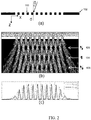
- the Talbot effect is a consequence of Fresnel diffraction, and the interference image (diffraction pattern) 104, indicated at arrow 1 as shown in Fig.
- a property of the Talbot effect is its response to off-axis illumination.
- d >> ⁇ linear gratings illuminated by an off-axis plane wave incident at angle ⁇
- multiple sources of off-axis illumination each generate their own set of laterally shifted grating self-images, and these self-images superpose. For small angles, these self-images all form at approximately the same distances, and the superimposed image contains information about the magnitude of illumination as well as direction.
- the incident angles of light rays striking the grating can be determined by measuring the shift in Talbot self-images.
- CMOS circuits allows for the construction of very fine features, on the order of a single wavelength of light, and so allows for the construction of metal diffraction gratings and photodiode arrays that are smaller than the wavelength of visible light.
- the self-images need to form within microns of the diffraction grating. This may require the diffraction grating to have a period of only a few wavelengths.
- Conventional analyses of diffraction are invalid at these dimensions; however, numerical simulations such as those used to generate Fig. 2 , confirm that, even for these geometries, diffraction generates Talbot-like self-images at regular distances. These periodic intensity patterns retain incident angle sensitivity.
- the challenge is to extract shifts in these periodic intensity patterns using structures on a pixel scale.
- the simplest approach to measuring these shifts is to place a small array of CCD or CMOS photosensors at the plane of self-image formation.
- the array captures the self-image directly, which can be used to determine the angle and intensity of incident light.
- the penetration depth of light in silicon limits the resolution of photodiodes to about 1 ⁇ m, making it difficult to resolve sub-micron features of the self-image.
- a micron-scale light-field imager device requires both a Talbot self-image generator and a structure that can analyzing these images.
- the entire device structure In order to achieve spatial resolution comparable with existing image sensors, the entire device structure must fit within an area that is at most tens of microns on a side. To produce a reasonably periodic self-image, the grating must have several periods within this area. Together these two constraints suggest using a grating with a period of only a few wavelengths. Contemporary planar photolithography techniques can easily achieve the resolution required to generate appropriate diffraction gratings. Numerical modeling and simulation can accurately predict behavior for finite gratings built on a single-micron scale.
- the high density imager array would require a pixel pitch of 1 ⁇ 4 the grating pitch (e.g., on the order of 200 nm) to effectively resolve the features of the Talbot image.
- the grating pitch e.g., on the order of 200 nm
- a solution provided by an aspect includes a second parallel analyzer grating 304 of identical period to the first grating 302 disposed at the self-image plane, as illustrated in Figs. 3a, 3b .
- the second (analyzer) grating 304 uses the Moire effect to filter the Talbot image.
- the intensity peaks align with gaps in the second grating as shown in Fig. 3b
- light passes through the analyzer grating 304.
- the bars of the analyzer grating block the light.
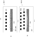
- Figure 4b shows an exemplary, diagrammatic illustration of such a structure 300-2 for extracting partial information about the diffraction pattern phase.
- Two metal gratings 302a, 302b are placed at a 90 degree lateral offset relative each other over a single, large well-diode 307 integrated into substrate 310.
- This approach decouples the design of the diodes from that of the gratings, allowing for better diodes.
- the finest features in this aspect are the gratings themselves rather than the photodiodes, the same class of structure can be built using lower resolution photolithography (i.e., in a larger feature size, cheaper manufacturing process).
- the device 400-2 is responsive only to angles in one direction.
- a second set of identical devices with gratings rotated by 90 degrees, in close proximity to the first were provided. This second set is responsible for measuring the angle information ignored by the first set of sensors.
- a complete angle-sensitive pixel (ASP) 500-1 composed of eight different sensors placed in close proximity is shown in Fig. 6b . Four sensors are responsible for the angle in the x-z plane; four more are needed for the angle in the y-z plane.
- diffraction-analyzer offsets of 0, d /4, d /2 and 3 d /4 were used.
- the analyzer gratings were positioned at the 1 ⁇ 2 Talbot distance, the smallest distance where self-images with periodicity identical to the diffraction grating are found.
- An 8x8 ASP array light field image sensor 500-2 manufactured in a digital 130 nm CMOS fabrication process is illustrated in the photomicrograph of Fig. 6a .
- the overall size of the exemplary eight-sensor ASP 500-1 is 20 ⁇ m by 40 ⁇ m, with each individual sensor being 10 ⁇ m square.
- the stacked diffraction gratings were built in wiring layers, above intrinsic p-n junction photodiodes.
- each grating in each of the eight sensors was a Ronchi ruling (equal width bars and gaps) using copper bars with a period of 880 nm. All other space was filled with silicon dioxide.
- One set of gratings was used to bus out the data generated, which eliminated the need for wiring lanes in the array. As the gratings provide a large number of bus lines, the eight ASP outputs are read in parallel.
- the grating separation, z was limited by available interconnect layer spacing, and pitch d chosen from numerical simulations to maximize modulation depth, m , for green (525 nm in vacuum, 350 nm in oxide) light.
- the top diffraction grating was positioned in the 6th metal layer and the analyzer grating in the 3rd metal layer, for a separation of 2 microns.
- a single p-n photodiode in each of the eight sensors measured the total light flux through the stacked gratings.
- a standard 3T active pixel sensor was used to buffer the photodiode outputs, and several multiplexers allowed access to each ASP individually.
- Figure 7 shows an illustrative aspect of a device 6000-1 similar to that shown in Fig. 5a in which three single diodes 6007, 6008, 6009 are disposed adjacent two grating layers 6001a, 6001b. Second grating layer 6001b is shifted relative to grating 6001a by 0, 1/3 and 2/3 of the grating period.
- a light field image detector 600-1 is illustrated in Fig. 8 .
- a second set of gratings 502a, 502b rotated by 90 degrees and interleaved between grating 402a, 402b are provided in close proximity thereto. This second set of gratings is responsible for measuring the angle information ignored by the first set of sensors.
- a light source (commercial green LED, with center wavelength of 525 nm and spectral width of 32 nm) was mounted on a variable angle arm at a fixed distance from the fabricated arrays. No additional collimation or filtering was performed, as a non-ideal illumination source better approximates real-world imaging applications.
- the self-images observed are a superposition of the intensity patterns produced by each wavelength.
- the spectral width of the source is relatively narrow and the path length differences, which make the Talbot patterns, are shorter than the source's coherence length, so we did not expect significant deviation in performance from our monochromatic, coherent simulations.
- Fine-pitch gratings are known to polarize the light they transmit.
- a recent study on the polarization-dependent Talbot effect in high-density gratings predicts that gratings with period of approximately 2.5 ⁇ should show significant polarization sensitivity.
- the Talbot self-images formed at the 1 ⁇ 2 Talbot distance by TE (electric field parallel to the grating lines) polarized light should be approximately twice as bright as those formed by TM (magnetic field parallel to the grating lines) polarized light.
- TE electric field parallel to the grating lines
- TM magnetic field parallel to the grating lines
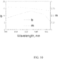
- This prediction was born out by measurement, as can be seen in Fig. 10 : b was only weakly sensitive to ⁇ over the range 400 nm to 620 nm.
- changes in wavelength significantly change the Talbot distances.
- the analyzer grating was not optimally positioned when ⁇ ⁇ 525 nm, so the observed self-images were blurred, and modulation depth, m , degraded.
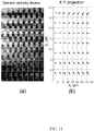
- the array could be used to accurately reconstruct the location of the light source in two dimensions, as shown in Fig. 12a , where the source was moved by 100 pm in the x-direction, and the computed incident angles reflect this. More strikingly, the array could be used to accurately localize the light source in the third, z direction, accurately capturing a 50 pm shift in the height of the source above the array, as shown in Fig. 129b.
- an array of ASPs is able to accurately reconstruct the three-dimensional structure of simple light sources, providing information beyond what is available from the intensity map available from a standard image sensor.
- Figure 4a shows a cross sectional schematic of a non-limiting exemplary device 300-1.
- the device includes a metal slit grating 301 and a substrate 310 with multiple linear arrays of two integrated, interleaved fingered diodes (A) 307, (B) 308 that are relatively shifted by 180 degrees (i.e., offset by zero and one-half period of the grating) relative to the grating.
- Multi-finger diodes advantageously provide maximum photon capture.
- Figure 13 shows an imaging device 500-1 based upon a three-diode structure according to a non-limiting exemplary aspect.
- the device includes a metal transmission grating 501 having multiple, periodic slit apertures 503.
- the light shadings indicated by reference numeral 504 do not represent any physical part of the device, rather merely the alignment between the grating and the diodes.
- the device further includes a single structure of three linear arrays of three interleaved diodes, 507, 508, 509, integrated in a substrate 510.
- the three illustrated diodes of diode array 507 are aligned with the grating (no offset) and thus will detect a zero degree phase shift in the interference pattern (not shown).
- the three illustrated diodes of diode array 508 are offset by 1/3 of the grating period and thus detect a 120 degree phase shift; while the three illustrated diodes of diode array 509 are offset by 2/3 of the grating period and thus detect a 240 degree phase shift.
- Figure 14 shows an alternate device arrangement 400-1 of diodes and grating according to a non-limiting, aspect.
- an integrated, single-interleaved set of four diodes 407, 408, 409, 411 are positioned offset by zero, 1/4, 1 ⁇ 2 and 3 ⁇ 4 of the grating 401 period providing respective phase shifts of 0°, 90°, 180° and 270°.
- the single-interleaved set of four diodes is different than, e.g., the two adjacent diode sets as shown in Figure 4a .
- the light shadow areas in the figure do not reflect any additional physical structure; rather, they only indicate alignment between diodes and metal.
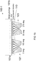
- Figure 15 shows a cross-sectional schematic of a detector device 100-1 according to an alternative, non-limiting exemplary aspect.
- Sensor device 100-1 incorporates one set of interleaved diodes 121 at 0 and 180 degrees relative to the grating and another set of interleaved diodes 123 at 90 and 270 degrees. This type of arrangement may prevent diode overlap.
- the two shifted gratings 101a, 101b are shown as darkly shaded while the lighter shading 103 beneath each grating is presented merely to show the alignment between the grating and the diodes and does not represent any physical structure of the device.
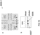
- Figure 16a shows a top view of components of a non-limiting, exemplary device aspect 8000-1 incorporating just two slits 8003 and two diodes 8007, 8008.
- Figure 16b is a cross-sectional view through the dashed line in Figure 12a . This design is compact, allowing for higher spatial resolution.
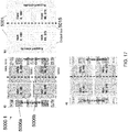
- Figures 17 (a-c) show top views of components of a non-limiting, exemplary full interleaved diode light-field sensor cell 5000-1, having gratings and diodes in both the vertical (5006a, b) and horizontal (5006c, d) orientations, which may be used to capture both azimuth and altitude information about the source object.
- Figure 17a illustrates the layout of diodes (e.g., n-type diffusion in p-substrate), wherein each set of vertically-oriented diodes 5006a, b contains a pair 5002, 5004 of interleaved diode arrays and each set of horizontally-oriented diodes 5006c, d contains a pair 5008, 5010 of interleaved diode arrays.
- Figure 17b shows the associated metal gratings 5001 with the same orientations as the corresponding diode arrays.
- the vertically-oriented gratings may be used as a data bus to carry information from each column to the edge of the array at 5015 without giving up area in the imager itself.
- the gratings may be used to tie many individual diodes to processing circuits away from the array itself. This maximizes the photosensitive area of the imager, recovering area lost to circuits required to convert light into electrical signals.
- Figure 17c shows an overlay of diodes and gratings shown in Figures 17a , b.
- Figure 15 which shows a cross-section of the horizontally-oriented detectors (i.e., along the dashed black line in Figures 17a-c ), illustrates that the relative alignment of the diodes and metal grating are shifted for the 0/180° cases versus the 90/270° case.
- Figure 18 shows an exemplary device aspect 2000-1 similar to that of 100-1 except that all diodes are shifted by 1/8 of the grating pitch, representing phase shifts of -45°, 135°, 45° and -135°.
- This figure illustrates that the precise alignment of diodes and metal is less important than the relative alignment of diodes to each other.
- the 1/8 period shift should have no appreciable effect on the function of the structures disclosed herein. This insensitivity applies to all structures disclosed herein, and to the alignment of secondary gratings in the "double grating" aspects described herein.
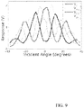
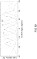
- Figure 19 graphically shows simulated photocurrents from four distinct diode arrays at 0, 90 180 and 270 degrees relative to a grating where the incident angle was swept from -30 to 30 degrees, according to an illustrative aspect of the invention.
- each diode shows multiple peaks, indicating that equations (1) may not necessarily lead to a unique angle extraction. This may be remedied by using multiple structures with different grating geometries (and therefore different values of "k"), placed adjacent to each other. If the mapping from incident angle to diode response is different, then different peaks of activity may be distinguished. This may then facilitate construction of a sensor that is able to cover the entire range of incident angles.
- Fig. 21 shows a device aspect 700-1 similar to that of device 100-1 in Fig. 15 , with the exception that the two sets of interleaved diffusion-type diodes 121, 123 (721, 723) are, respectively, disposed in two single, large well-diodes 724, 725.
- crosstalk observed in the sub-micron size diffusion-type diodes may be reduced, since the large photodiodes collect the electrons and holes generated by photons that penetrate into the substrate beyond the thin, interleaved diodes.
- the large well diodes are fabricated deep enough to enclose the interleaved diodes but shallow enough to catch electrons.
- Interleaved/deep-well diodes can also be incorporated into devices which rely on multiple sets of gratings for angle sensitivity.
- a device 800-1 using two gratings placed 1 ⁇ 2 Talbot distance apart vertically and photodiodes at the 1 st Talbot distance is shown in Fig. 22 .
- the large-well photodiodes measure the total light flux passing through the two gratings.
- the mode of operation is identical to that of the basic multiple grating device.
- the interleaved photodiodes help locate the lateral offset of the periodic intensity pattern with greater accuracy. This provides improved characterization of incident angle around a set of known angles without interfering with basic function.
- Another aspect useful for understanding the invention is directed to a method for extracting incident light-angle information from a light source object.
- the ability to detect said angle information has applications pertaining, but not limited to, sensor networks and sensor arrays; direction and/or speed of motion detection of objects passing over a sensor such as, for example, the direction and speed of a vehicle passing over a sensor embedded in road pavement; detection/reception of multiple data streams from separate transmitters in a free-space optical communication system; bio-medical applications such as, e.g., detection of individual fluorescent cells in tissue containing such fluorescent cells, and others that would be appreciated by persons skilled in the art.
- the method may be accomplished entirely without the use of lenses, and performed with image sensors on the physical scale of silicon integrated circuits.
- a sensor array as described herein above may be positioned adjacent a piece of tissue containing fluorescent cells. Each cell would generate light whose incident angles (into the sensor) would indicate the cell's location in three-dimensional space. By triangulating back from the angles detected by each sensor in the array, as schematically illustrated in Fig. 1b , the location of individual fluorescent cells could be detected, as well as changes in their fluorescence independently from the other fluorescent cells.
- many image sensor arrays could be deployed as part of a larger array of tissue culture chambers. Each individual image sensor would provide monitoring of its respective sample, providing high-throughput analysis of many samples at once.
- the method may be accomplished using an imaging sensor in combination with a lens system, which may be advantageous to image more distant objects.
- an object 1402 at the focal plane of the lens system 1405 will appear completely in focus on the surface 1406 of the sensor array 1407, and will appear to have an even distribution of angles of incidence 1409.
- the array acts like a normal CMOS imager.
- Objects more distant than the focal plane of the lens system will generate blurred images on the array, but the blurring will show a variable set of incident angles that converge on the focal plane of the object, as shown in Fig. 20b .
- Objects closer than the focal depth of the lens system will also appear blurred, but with a divergent set of incident angles, indicating a focal depth behind the array, as shown in Fig. 20c .
- the imager can extract useful information that can be used to describe the location of objects both closer and farther away than the optical focal plane of the lens system.
- the imager by detecting incident angle, can extract information about an object region that is thicker than the normal depth of focus associated with a given lens system.
- this information may be used, e.g., to reconstruct the three-dimensional structure of a scene or, to computationally refocus the image to different focal depths after the image has been captured.
- the data from such an imager may be used to simultaneously refocus different parts of the image to different depths.
- a single light-emitting object will generate a sensor response that maps to a single incident angle, multiple light sources will result in a linear superposition of responses, each of which depends on the incident angle of each source.
- a given pixel design will work effectively for a limited range of wavelengths.
- this wavelength is known in advance, such as in fluorescent microscopy or communication systems using known LEDs, the gratings can be designed appropriately as known in the art.
- a color filter 1430 may be required in conjunction with the chip to limit the incident light wavelengths to the appropriate range.
- Modern imager processes typically include such color filters; thus they could be incorporated into the basic design.
- multiple color filter layers typically red, green and blue
- using these filters in conjunction with three separately tuned sets of gratings would permit light-field imaging in color.
- a response r(x s ,y s ,a) (where x s and y s are as above, and a is an index from 1 to 8 representing the phase associated with the diode) to any given stimulus s(x,y,z).
- FIG. 15a, b An example of this is shown in Figures 15a, b for two 16x16 arrays, one where each pixel simply detects light, and the other where each pixel contains two fingered diodes and a metal grating, such that sets of four pixels form a cell, as shown in Figure 5c .
- the grating based design For a focal plane four pixel widths from the imager plane, the grating based design generates a conversion matrix A whose singular values are consistently larger, by as much as a factor of 100 than those for a normal imager.
- calculating the pseudo-inverse for a grating-based imager yields a more accurate, lower noise result than with a normal imager.
- a second result of this approach is that one can calculate an error term based upon using the pseudo inverse.
- the method described herein above need not be applied to the entire image, but can be applied to subsections of the image such that they can be refocused independently and/or their range found, leading to better overall focus and/or a range map across the image.
- Another exemplary application pertains to imaging the three dimensional structure of fluorescing cells in tissue. Since the goal of such an application would be to be able to independently quantify the fluorescence of multiple cells at different focal planes, refocusing is not an appropriate approach. However, if one adds the two additional constraints: i) that all entries in s must be strictly positive (there is no such thing as negative fluorescence), and ii) that the fluorescent sources are relatively sparsely distributed in the volume being imaged, one may assume that the number of fluorescent cells is smaller than N 2 , the number of pixels. If this holds true, then one can find each of these sources iteratively and in order of brightness as follows:
- Each iteration of this algorithm finds the most likely dominant point source of the light field seen in r , includes that source in the estimate of the stimulus, s', then removes that portion of the effect from r permitting the algorithm to find the next most dominant source.
Landscapes
- Physics & Mathematics (AREA)
- General Physics & Mathematics (AREA)
- Health & Medical Sciences (AREA)
- Electromagnetism (AREA)
- Engineering & Computer Science (AREA)
- Radar, Positioning & Navigation (AREA)
- Remote Sensing (AREA)
- Life Sciences & Earth Sciences (AREA)
- Nuclear Medicine, Radiotherapy & Molecular Imaging (AREA)
- Chemical & Material Sciences (AREA)
- Analytical Chemistry (AREA)
- Biochemistry (AREA)
- General Health & Medical Sciences (AREA)
- Immunology (AREA)
- Pathology (AREA)
- Solid State Image Pick-Up Elements (AREA)
- Investigating Or Analysing Materials By Optical Means (AREA)
- Holo Graphy (AREA)
- Spectrometry And Color Measurement (AREA)
Claims (2)
- Dispositif sans lentille, de pixel sensible à l'angle (ASP), sensible à une intensité et un angle incident de la lumière, comprenant :une structure de support de dispositif ;une première structure périodique de diffraction de la lumière ayant une période p1, disposée dans la structure de support ;une seconde structure périodique de diffraction de la lumière ayant une période p2, orientée parallèlement à la première structure périodique de diffraction de la lumière et disposée dans la structure de support à une deuxième distance Talbot sélectionnée de la première structure périodique à la seconde structure périodique, zT2 = (m2 /n2 ) (2p1 2/λ), en dessous de la première structure périodique de diffraction de la lumière, où m2, n2 sont des entiers positifs, et où p1 est supérieur ou égal à λ, qui est la longueur d'onde d'un front d'onde incident monochromatique, plan, sur la première structure périodique de diffraction de la lumière ; etun capteur disposé dans la structure de support en dessous de la seconde structure périodique, le capteur comprenant au moins deux ensembles de diodes entrelacées de type à diffusion respectivement déplacées latéralement depuis la première structure périodique de diffraction de la lumière d'une distance np1/m, où n peut prendre les valeurs 0, 1, 2, 3, 4,5, 6, 7, 8 et m peut prendre les valeurs 2, 3, 4, 8 ; le capteur étant disposé dans la structure de support à une première distance Talbot sélectionnée zT1 = (m1 /n1 )(2p1 2/λ), en dessous de la première structure périodique de diffraction de la lumière, où m1, n1 sont des entiers positifs, et où zT2 est inférieur à zT1.
- Dispositif selon la revendication 1, le dispositif étant une structure à semi-conducteurs CMOS intégrée.
Priority Applications (1)
| Application Number | Priority Date | Filing Date | Title |
|---|---|---|---|
| EP21153209.8A EP3836215A1 (fr) | 2008-07-25 | 2009-07-24 | Capteur d'images à champ lumineux, procédé et applications |
Applications Claiming Priority (2)
| Application Number | Priority Date | Filing Date | Title |
|---|---|---|---|
| US8368808P | 2008-07-25 | 2008-07-25 | |
| PCT/US2009/051660 WO2010044943A2 (fr) | 2008-07-25 | 2009-07-24 | Capteur d'images à champ lumineux, procédé et applications |
Related Child Applications (1)
| Application Number | Title | Priority Date | Filing Date |
|---|---|---|---|
| EP21153209.8A Division EP3836215A1 (fr) | 2008-07-25 | 2009-07-24 | Capteur d'images à champ lumineux, procédé et applications |
Publications (3)
| Publication Number | Publication Date |
|---|---|
| EP2311092A2 EP2311092A2 (fr) | 2011-04-20 |
| EP2311092A4 EP2311092A4 (fr) | 2013-11-20 |
| EP2311092B1 true EP2311092B1 (fr) | 2021-01-27 |
Family
ID=42107123
Family Applications (2)
| Application Number | Title | Priority Date | Filing Date |
|---|---|---|---|
| EP09820950.5A Active EP2311092B1 (fr) | 2008-07-25 | 2009-07-24 | Capteur d'images à champ lumineux, procédé et applications |
| EP21153209.8A Pending EP3836215A1 (fr) | 2008-07-25 | 2009-07-24 | Capteur d'images à champ lumineux, procédé et applications |
Family Applications After (1)
| Application Number | Title | Priority Date | Filing Date |
|---|---|---|---|
| EP21153209.8A Pending EP3836215A1 (fr) | 2008-07-25 | 2009-07-24 | Capteur d'images à champ lumineux, procédé et applications |
Country Status (5)
| Country | Link |
|---|---|
| US (2) | US8530811B2 (fr) |
| EP (2) | EP2311092B1 (fr) |
| KR (1) | KR101629044B1 (fr) |
| CN (1) | CN102099916B (fr) |
| WO (1) | WO2010044943A2 (fr) |
Families Citing this family (71)
| Publication number | Priority date | Publication date | Assignee | Title |
|---|---|---|---|---|
| US9494419B2 (en) | 2009-07-31 | 2016-11-15 | Hewlett Packard Enterprise Development Lp | Beam direction sensor |
| US9740019B2 (en) | 2010-02-02 | 2017-08-22 | Apple Inc. | Integrated structured-light projector |
| LU91688B1 (en) * | 2010-05-17 | 2011-11-18 | Iee Sarl | Scanning 3D imager |
| KR101790601B1 (ko) * | 2010-08-03 | 2017-10-26 | 코넬 유니버시티 | 각 감지 픽셀(asp)에 기초한 이미지 처리 시스템, 방법, 및 응용들 |
| JP2012064703A (ja) * | 2010-09-15 | 2012-03-29 | Sony Corp | 撮像素子および撮像装置 |
| EP2633277B1 (fr) * | 2010-10-27 | 2020-06-17 | Cornell University | Dispositif a pixels sensible à l'angle |
| WO2012056437A1 (fr) * | 2010-10-29 | 2012-05-03 | École Polytechnique Fédérale De Lausanne (Epfl) | Système de réseau de capteurs omnidirectionnels |
| US9146403B2 (en) * | 2010-12-01 | 2015-09-29 | Massachusetts Institute Of Technology | Content-adaptive parallax barriers for automultiscopic display |
| CN103035656B (zh) * | 2011-03-15 | 2015-08-12 | 深圳光启智能光子技术有限公司 | 一种基于cmos加工工艺的光传感系统 |
| CN102143332B (zh) * | 2011-04-20 | 2013-03-20 | 中国科学院半导体研究所 | 基于标准cmos工艺的彩色图像传感器 |
| CN102865999B (zh) * | 2011-07-08 | 2015-03-04 | 中国科学院微电子研究所 | Led光学特性检测方法及检测装置 |
| US8749796B2 (en) | 2011-08-09 | 2014-06-10 | Primesense Ltd. | Projectors of structured light |
| CN103782200A (zh) * | 2011-09-09 | 2014-05-07 | 欧司朗股份有限公司 | 改进的占用传感器装置 |
| WO2013046820A1 (fr) * | 2011-09-28 | 2013-04-04 | 富士フイルム株式会社 | Capteur d'image et dispositif de formation d'image |
| CN203385981U (zh) * | 2012-03-15 | 2014-01-08 | 普莱姆森斯有限公司 | 结构光的投影机 |
| WO2014048831A1 (fr) * | 2012-09-27 | 2014-04-03 | Snap-On Equipment Srl A Unico Socio | Procédé et système d'inspection, de maintenance ou de réparation d'un véhicule ou d'une pièce d'un véhicule |
| US10514509B2 (en) * | 2013-01-10 | 2019-12-24 | The Regents Of The University Of Colorado, A Body Corporate | Method and apparatus for optical waveguide-to-semiconductor coupling and optical vias for monolithically integrated electronic and photonic circuits |
| US9110240B2 (en) | 2013-03-05 | 2015-08-18 | Rambus Inc. | Phase gratings with odd symmetry for high-resolution lensed and lensless optical sensing |
| CN106170822B (zh) * | 2013-12-23 | 2020-03-24 | 特拉华大学 | 3d光场相机和摄影方法 |
| CN103715215B (zh) * | 2013-12-30 | 2018-10-16 | 上海集成电路研发中心有限公司 | 一种对角度敏感的图像像素单元 |
| WO2015157097A1 (fr) | 2014-04-09 | 2015-10-15 | Rambus Inc. | Détecteur de changement d'images à faible consommation |
| EP3137935B1 (fr) | 2014-04-30 | 2023-07-05 | Hewlett-Packard Development Company, L.P. | Appareil d'imagerie utilisant un éclairage basé sur la diffraction |
| CN105472233B (zh) * | 2014-09-09 | 2019-01-18 | 北京智谷技术服务有限公司 | 光场采集控制方法和装置、光场采集设备 |
| EP3271747B1 (fr) | 2015-03-17 | 2022-05-25 | Cornell University | Appareil d'imagerie à profondeur de champ, procédés et applications |
| US10404908B2 (en) | 2015-07-13 | 2019-09-03 | Rambus Inc. | Optical systems and methods supporting diverse optical and computational functions |
| US10284825B2 (en) | 2015-09-08 | 2019-05-07 | Rambus Inc. | Systems with integrated refractive and diffractive optics |
| WO2017081542A2 (fr) * | 2015-11-11 | 2017-05-18 | Scopio Lab Ltd. | Microscopes de calcul et procédés de génération d'une image dans des conditions d'éclairage différentes |
| EP3408585B1 (fr) * | 2016-01-26 | 2020-12-09 | Heptagon Micro Optics Pte. Ltd. | Module d'éclairage multimode et procédé associé |
| EP3420535B1 (fr) * | 2016-02-26 | 2022-09-07 | University Of Southern California | Imagerie volumétrique optimisée à éclairage de volume sélectif et détection de champ lumineux |
| US10983275B2 (en) | 2016-03-21 | 2021-04-20 | The Regents Of The University Of Colorado, A Body Corporate | Method and apparatus for optical waveguide-to-semiconductor coupling for integrated photonic circuits |
| DE102016208841B4 (de) * | 2016-05-23 | 2020-12-31 | Fraunhofer-Gesellschaft zur Förderung der angewandten Forschung e.V. | Farbsensor mit winkelselektiven Strukturen |
| JP7120929B2 (ja) * | 2016-06-07 | 2022-08-17 | エアリー3ディー インコーポレイティド | 深度取得及び3次元撮像のためのライトフィールド撮像デバイス及び方法 |
| EP4016992A3 (fr) * | 2016-07-13 | 2022-08-24 | Sony Group Corporation | Appareil d'imagerie, dispositif d'imagerie et appareil de traitement d'images |
| US10462377B2 (en) * | 2016-07-29 | 2019-10-29 | Nokia Of America Corporation | Single-aperture multi-sensor lensless compressive image acquisition |
| KR102721072B1 (ko) * | 2016-11-01 | 2024-10-24 | 삼성전자주식회사 | 분광 측정 장치 및 분광 측정 장치를 이용한 분광 측정 방법 |
| IL251636B (en) | 2017-04-06 | 2018-02-28 | Yoav Berlatzky | Coherence camera system and method thereof |
| WO2019018851A1 (fr) * | 2017-07-21 | 2019-01-24 | California Institute Of Technology | Appareil photographique plan ultramince sans lentille |
| US11882371B2 (en) * | 2017-08-11 | 2024-01-23 | California Institute Of Technology | Lensless 3-dimensional imaging using directional sensing elements |
| JP6803989B2 (ja) * | 2017-08-15 | 2020-12-23 | ソニーセミコンダクタソリューションズ株式会社 | 固体撮像装置及びその駆動方法 |
| US10153614B1 (en) | 2017-08-31 | 2018-12-11 | Apple Inc. | Creating arbitrary patterns on a 2-D uniform grid VCSEL array |
| US11223787B2 (en) | 2017-10-19 | 2022-01-11 | Sony Corporation | Information processing apparatus, information processing method, and imaging apparatus |
| US11451715B2 (en) | 2017-10-19 | 2022-09-20 | Sony Corporation | Imaging apparatus, exposure controlling method, and imaging device |
| JPWO2019078337A1 (ja) | 2017-10-19 | 2020-12-17 | ソニー株式会社 | 撮像装置および方法、並びに、画像処理装置および方法 |
| JP7156297B2 (ja) | 2017-10-19 | 2022-10-19 | ソニーグループ株式会社 | 撮像素子、画像処理装置、画像処理方法、および、プログラム |
| WO2019078339A1 (fr) | 2017-10-19 | 2019-04-25 | ソニー株式会社 | Appareil électronique |
| US11202062B2 (en) * | 2017-11-21 | 2021-12-14 | University Of New Hampshire | Methods and systems of determining quantum efficiency of a camera |
| JP7245835B2 (ja) * | 2017-12-05 | 2023-03-24 | エアリー3ディー インコーポレイティド | 奥行取得のためのライトフィールド画像処理方法 |
| CN112106343A (zh) | 2018-03-29 | 2020-12-18 | 索尼公司 | 信息处理装置、信息处理方法、程序和信息处理系统 |
| US11422292B1 (en) * | 2018-06-10 | 2022-08-23 | Apple Inc. | Super-blazed diffractive optical elements with sub-wavelength structures |
| CN108924407B (zh) * | 2018-06-15 | 2020-12-18 | 深圳奥比中光科技有限公司 | 一种深度成像方法及系统 |
| CN109187375A (zh) * | 2018-08-17 | 2019-01-11 | 西安交通大学 | 一种基于标准cmos工艺的芯片级光谱检测器件 |
| CN110891131B (zh) * | 2018-09-10 | 2025-03-18 | 北京小米移动软件有限公司 | 摄像头模组、处理方法及装置、电子设备、存储介质 |
| US10638061B2 (en) | 2018-09-18 | 2020-04-28 | Analog Devices Global Unlimited Company | Active-pixel image sensor |
| CN113167857B (zh) * | 2018-12-10 | 2023-03-24 | Abb瑞士股份有限公司 | 雷达传感器以及使用雷达传感器的机器人 |
| JP7262236B2 (ja) * | 2019-02-04 | 2023-04-21 | キヤノン株式会社 | 撮像装置およびその制御方法 |
| US11460576B2 (en) * | 2019-04-18 | 2022-10-04 | Beijing Voyager Technology Co., Ltd. | Transmitter having beam shifter for light detection and ranging (LIDAR) |
| US11889199B2 (en) * | 2019-06-04 | 2024-01-30 | Sony Group Corporation | Imaging device, signal processing device, signal processing method, program, and imaging apparatus |
| TW202101035A (zh) | 2019-06-05 | 2021-01-01 | 加拿大商艾瑞3D股份有限公司 | 用於3d感測之光場成像裝置及方法 |
| CN110363205B (zh) * | 2019-06-25 | 2021-06-22 | 浙江大学 | 一种基于Talbot效应光学卷积的图像特征提取系统及方法 |
| CN112770020A (zh) * | 2019-11-05 | 2021-05-07 | 北京小米移动软件有限公司 | 图像传感模组、方法、装置、电子设备及介质 |
| EP3825659B1 (fr) | 2019-11-19 | 2023-11-08 | CSEM Centre Suisse D'electronique Et De Microtechnique SA | Capteur de position |
| CN111229342B (zh) * | 2020-01-17 | 2022-02-11 | 上海新微技术研发中心有限公司 | 基于cmos图像传感的光栅波导多微流道芯片的制造方法 |
| US11721774B2 (en) | 2020-02-27 | 2023-08-08 | Taiwan Semiconductor Manufacturing Company, Ltd. | Full well capacity for image sensor |
| CN113314551A (zh) | 2020-02-27 | 2021-08-27 | 台湾积体电路制造股份有限公司 | 图像传感器及其形成方法 |
| US11754767B1 (en) | 2020-03-05 | 2023-09-12 | Apple Inc. | Display with overlaid waveguide |
| WO2022011333A1 (fr) * | 2020-07-10 | 2022-01-13 | Voyant Photonics, Inc. | Réseau d'émetteurs |
| US12429702B2 (en) | 2020-11-10 | 2025-09-30 | Airy3D Inc. | Imaging systems and methods for dual depth and polarization sensing |
| WO2022197339A1 (fr) | 2021-03-17 | 2022-09-22 | Apple Inc. | Émetteurs à base de guide d'ondes à éclairage réglable |
| CN113819998B (zh) * | 2021-09-18 | 2024-01-16 | 中北大学 | 一种基于二维单层光栅结构的多维角振动传感器 |
| US11662526B1 (en) * | 2021-12-09 | 2023-05-30 | Visera Technologies Company Ltd. | Optical structure |
| WO2024178377A1 (fr) * | 2023-02-23 | 2024-08-29 | The Board Of Trustees Of The Leland Stanford Junior University | Imagerie de texture utilisant des pixels sensibles à l'angle |
Citations (1)
| Publication number | Priority date | Publication date | Assignee | Title |
|---|---|---|---|---|
| US20060044429A1 (en) * | 2004-08-30 | 2006-03-02 | Sony Corporation | Information acquiring method, information acquiring apparatus, semiconductor device comprising array of plurality of unit components for detecting physical quantity distribution, and semiconductor manufacturing method |
Family Cites Families (13)
| Publication number | Priority date | Publication date | Assignee | Title |
|---|---|---|---|---|
| US4915463A (en) * | 1988-10-18 | 1990-04-10 | The United States Of America As Represented By The Department Of Energy | Multilayer diffraction grating |
| US5812629A (en) * | 1997-04-30 | 1998-09-22 | Clauser; John F. | Ultrahigh resolution interferometric x-ray imaging |
| CA2351721C (fr) * | 1998-11-20 | 2004-02-24 | California Institute Of Technology | Capteur a puits quantique a fentes |
| JP4445397B2 (ja) * | 2002-12-26 | 2010-04-07 | 敦 百生 | X線撮像装置および撮像方法 |
| JP4551624B2 (ja) * | 2003-03-14 | 2010-09-29 | 株式会社リコー | 傾きセンサ、傾き測定装置、光ピックアップ装置及び光ディスク装置 |
| JP4233089B2 (ja) | 2003-08-12 | 2009-03-04 | 株式会社リコー | 傾きセンサ、光ピックアップ装置及び光ディスク装置 |
| US7800823B2 (en) * | 2004-12-06 | 2010-09-21 | Moxtek, Inc. | Polarization device to polarize and further control light |
| EP1731099A1 (fr) * | 2005-06-06 | 2006-12-13 | Paul Scherrer Institut | Interféromètre pour l'imagerie et la tomographie à contraste de phase avec une source de rayons X incohérente et polychromatique |
| JP4984634B2 (ja) * | 2005-07-21 | 2012-07-25 | ソニー株式会社 | 物理情報取得方法および物理情報取得装置 |
| WO2007125833A1 (fr) * | 2006-04-24 | 2007-11-08 | The University Of Tokyo | Dispositif de recuperation d'images radiologiques et procede de recuperation d'images radiologiques |
| CN101135575A (zh) * | 2007-10-15 | 2008-03-05 | 中国科学技术大学 | 具有双反射镜的直接计数式变栅距单光栅光位移传感器 |
| US8809758B2 (en) * | 2008-07-25 | 2014-08-19 | Cornell University | Light field image sensor with an angle-sensitive pixel (ASP) device |
| WO2012145566A2 (fr) * | 2011-04-20 | 2012-10-26 | California Institute Of Technology | Dispositifs d'imagerie à éclairement talbot, systèmes et procédés d'ajustement du plan focal |
-
2009
- 2009-07-24 EP EP09820950.5A patent/EP2311092B1/fr active Active
- 2009-07-24 WO PCT/US2009/051660 patent/WO2010044943A2/fr not_active Ceased
- 2009-07-24 KR KR1020117004231A patent/KR101629044B1/ko active Active
- 2009-07-24 US US13/055,566 patent/US8530811B2/en active Active
- 2009-07-24 CN CN2009801374269A patent/CN102099916B/zh active Active
- 2009-07-24 EP EP21153209.8A patent/EP3836215A1/fr active Pending
-
2014
- 2014-08-18 US US14/462,039 patent/US9658060B2/en active Active
Patent Citations (1)
| Publication number | Priority date | Publication date | Assignee | Title |
|---|---|---|---|---|
| US20060044429A1 (en) * | 2004-08-30 | 2006-03-02 | Sony Corporation | Information acquiring method, information acquiring apparatus, semiconductor device comprising array of plurality of unit components for detecting physical quantity distribution, and semiconductor manufacturing method |
Also Published As
| Publication number | Publication date |
|---|---|
| US9658060B2 (en) | 2017-05-23 |
| US20110174998A1 (en) | 2011-07-21 |
| EP2311092A2 (fr) | 2011-04-20 |
| KR101629044B1 (ko) | 2016-06-09 |
| CN102099916B (zh) | 2013-07-31 |
| CN102099916A (zh) | 2011-06-15 |
| EP3836215A1 (fr) | 2021-06-16 |
| WO2010044943A2 (fr) | 2010-04-22 |
| WO2010044943A3 (fr) | 2010-07-22 |
| KR20110036844A (ko) | 2011-04-11 |
| US20150125943A1 (en) | 2015-05-07 |
| EP2311092A4 (fr) | 2013-11-20 |
| US8530811B2 (en) | 2013-09-10 |
Similar Documents
| Publication | Publication Date | Title |
|---|---|---|
| EP2311092B1 (fr) | Capteur d'images à champ lumineux, procédé et applications | |
| EP2633277B1 (fr) | Dispositif a pixels sensible à l'angle | |
| US8809758B2 (en) | Light field image sensor with an angle-sensitive pixel (ASP) device | |
| JP6463582B2 (ja) | 符号化ローカライゼーションシステム、方法および装置 | |
| EP3423858B1 (fr) | Système et procédé d'imagerie 3d | |
| EP3466052B1 (fr) | Dispositif et procédé d'imagerie à champ lumineux d'acquisition de profondeur et d'imagerie tridimensionnelle | |
| KR101790601B1 (ko) | 각 감지 픽셀(asp)에 기초한 이미지 처리 시스템, 방법, 및 응용들 | |
| US10319764B2 (en) | Image sensor and electronic device | |
| WO2019075335A1 (fr) | Caméras à œil composite sans lentille basées sur des métasurfaces sensibles à l'angle | |
| US20140198183A1 (en) | Sensing pixel and image sensor including same | |
| WO2006071874A1 (fr) | Imageur spectral et son procede de fabrication | |
| KR100783335B1 (ko) | 입사광의 측정 방법 및 그것을 이용한 분광 기구를 갖는센서 | |
| Wang et al. | Angle sensitive pixels in CMOS for lensless 3D imaging | |
| JP2017229001A (ja) | 撮像装置および測距装置 | |
| US6563947B1 (en) | Application specified integrated circuit for use in wavefront detection | |
| KR20100076222A (ko) | 이미지 센서에서 마이크로 렌즈의 위치 변경 장치 및 방법 | |
| US10998460B2 (en) | High information content imaging using Mie photo sensors | |
| Wang et al. | Fluorescent imaging and localization with angle sensitive pixel arrays in standard CMOS | |
| JP6260950B2 (ja) | 屈折率測定方法 | |
| Bray et al. | Front-side illuminated CMOS spectral pixel response and modulation transfer function characterization: impact of pixel layout details and pixel depletion volume | |
| JP2023011110A (ja) | 2波長赤外線センサ、及び撮像システム | |
| Gill et al. | Scaling properties of well-tiled PFCAs |
Legal Events
| Date | Code | Title | Description |
|---|---|---|---|
| PUAI | Public reference made under article 153(3) epc to a published international application that has entered the european phase |
Free format text: ORIGINAL CODE: 0009012 |
|
| 17P | Request for examination filed |
Effective date: 20110201 |
|
| AK | Designated contracting states |
Kind code of ref document: A2 Designated state(s): AT BE BG CH CY CZ DE DK EE ES FI FR GB GR HR HU IE IS IT LI LT LU LV MC MK MT NL NO PL PT RO SE SI SK SM TR |
|
| AX | Request for extension of the european patent |
Extension state: AL BA RS |
|
| RIN1 | Information on inventor provided before grant (corrected) |
Inventor name: WANG, ALBERT Inventor name: MOLNAR, ALYOSHA |
|
| DAX | Request for extension of the european patent (deleted) | ||
| A4 | Supplementary search report drawn up and despatched |
Effective date: 20131023 |
|
| RIC1 | Information provided on ipc code assigned before grant |
Ipc: H01L 27/144 20060101ALI20131017BHEP Ipc: H01L 27/146 20060101AFI20131017BHEP |
|
| STAA | Information on the status of an ep patent application or granted ep patent |
Free format text: STATUS: EXAMINATION IS IN PROGRESS |
|
| 17Q | First examination report despatched |
Effective date: 20180517 |
|
| GRAP | Despatch of communication of intention to grant a patent |
Free format text: ORIGINAL CODE: EPIDOSNIGR1 |
|
| STAA | Information on the status of an ep patent application or granted ep patent |
Free format text: STATUS: GRANT OF PATENT IS INTENDED |
|
| INTG | Intention to grant announced |
Effective date: 20201120 |
|
| GRAS | Grant fee paid |
Free format text: ORIGINAL CODE: EPIDOSNIGR3 |
|
| GRAA | (expected) grant |
Free format text: ORIGINAL CODE: 0009210 |
|
| STAA | Information on the status of an ep patent application or granted ep patent |
Free format text: STATUS: THE PATENT HAS BEEN GRANTED |
|
| AK | Designated contracting states |
Kind code of ref document: B1 Designated state(s): AT BE BG CH CY CZ DE DK EE ES FI FR GB GR HR HU IE IS IT LI LT LU LV MC MK MT NL NO PL PT RO SE SI SK SM TR |
|
| REG | Reference to a national code |
Ref country code: GB Ref legal event code: FG4D |
|
| REG | Reference to a national code |
Ref country code: CH Ref legal event code: EP |
|
| REG | Reference to a national code |
Ref country code: AT Ref legal event code: REF Ref document number: 1360186 Country of ref document: AT Kind code of ref document: T Effective date: 20210215 |
|
| REG | Reference to a national code |
Ref country code: IE Ref legal event code: FG4D |
|
| REG | Reference to a national code |
Ref country code: DE Ref legal event code: R096 Ref document number: 602009063314 Country of ref document: DE |
|
| REG | Reference to a national code |
Ref country code: NL Ref legal event code: MP Effective date: 20210127 |
|
| REG | Reference to a national code |
Ref country code: LT Ref legal event code: MG9D |
|
| REG | Reference to a national code |
Ref country code: AT Ref legal event code: MK05 Ref document number: 1360186 Country of ref document: AT Kind code of ref document: T Effective date: 20210127 |
|
| PG25 | Lapsed in a contracting state [announced via postgrant information from national office to epo] |
Ref country code: PT Free format text: LAPSE BECAUSE OF FAILURE TO SUBMIT A TRANSLATION OF THE DESCRIPTION OR TO PAY THE FEE WITHIN THE PRESCRIBED TIME-LIMIT Effective date: 20210527 Ref country code: BG Free format text: LAPSE BECAUSE OF FAILURE TO SUBMIT A TRANSLATION OF THE DESCRIPTION OR TO PAY THE FEE WITHIN THE PRESCRIBED TIME-LIMIT Effective date: 20210427 Ref country code: NL Free format text: LAPSE BECAUSE OF FAILURE TO SUBMIT A TRANSLATION OF THE DESCRIPTION OR TO PAY THE FEE WITHIN THE PRESCRIBED TIME-LIMIT Effective date: 20210127 Ref country code: NO Free format text: LAPSE BECAUSE OF FAILURE TO SUBMIT A TRANSLATION OF THE DESCRIPTION OR TO PAY THE FEE WITHIN THE PRESCRIBED TIME-LIMIT Effective date: 20210427 Ref country code: FI Free format text: LAPSE BECAUSE OF FAILURE TO SUBMIT A TRANSLATION OF THE DESCRIPTION OR TO PAY THE FEE WITHIN THE PRESCRIBED TIME-LIMIT Effective date: 20210127 Ref country code: GR Free format text: LAPSE BECAUSE OF FAILURE TO SUBMIT A TRANSLATION OF THE DESCRIPTION OR TO PAY THE FEE WITHIN THE PRESCRIBED TIME-LIMIT Effective date: 20210428 Ref country code: HR Free format text: LAPSE BECAUSE OF FAILURE TO SUBMIT A TRANSLATION OF THE DESCRIPTION OR TO PAY THE FEE WITHIN THE PRESCRIBED TIME-LIMIT Effective date: 20210127 Ref country code: LT Free format text: LAPSE BECAUSE OF FAILURE TO SUBMIT A TRANSLATION OF THE DESCRIPTION OR TO PAY THE FEE WITHIN THE PRESCRIBED TIME-LIMIT Effective date: 20210127 |
|
| PG25 | Lapsed in a contracting state [announced via postgrant information from national office to epo] |
Ref country code: AT Free format text: LAPSE BECAUSE OF FAILURE TO SUBMIT A TRANSLATION OF THE DESCRIPTION OR TO PAY THE FEE WITHIN THE PRESCRIBED TIME-LIMIT Effective date: 20210127 Ref country code: LV Free format text: LAPSE BECAUSE OF FAILURE TO SUBMIT A TRANSLATION OF THE DESCRIPTION OR TO PAY THE FEE WITHIN THE PRESCRIBED TIME-LIMIT Effective date: 20210127 Ref country code: PL Free format text: LAPSE BECAUSE OF FAILURE TO SUBMIT A TRANSLATION OF THE DESCRIPTION OR TO PAY THE FEE WITHIN THE PRESCRIBED TIME-LIMIT Effective date: 20210127 Ref country code: SE Free format text: LAPSE BECAUSE OF FAILURE TO SUBMIT A TRANSLATION OF THE DESCRIPTION OR TO PAY THE FEE WITHIN THE PRESCRIBED TIME-LIMIT Effective date: 20210127 |
|
| PG25 | Lapsed in a contracting state [announced via postgrant information from national office to epo] |
Ref country code: IS Free format text: LAPSE BECAUSE OF FAILURE TO SUBMIT A TRANSLATION OF THE DESCRIPTION OR TO PAY THE FEE WITHIN THE PRESCRIBED TIME-LIMIT Effective date: 20210527 |
|
| REG | Reference to a national code |
Ref country code: DE Ref legal event code: R097 Ref document number: 602009063314 Country of ref document: DE |
|
| PG25 | Lapsed in a contracting state [announced via postgrant information from national office to epo] |
Ref country code: EE Free format text: LAPSE BECAUSE OF FAILURE TO SUBMIT A TRANSLATION OF THE DESCRIPTION OR TO PAY THE FEE WITHIN THE PRESCRIBED TIME-LIMIT Effective date: 20210127 Ref country code: CZ Free format text: LAPSE BECAUSE OF FAILURE TO SUBMIT A TRANSLATION OF THE DESCRIPTION OR TO PAY THE FEE WITHIN THE PRESCRIBED TIME-LIMIT Effective date: 20210127 Ref country code: SM Free format text: LAPSE BECAUSE OF FAILURE TO SUBMIT A TRANSLATION OF THE DESCRIPTION OR TO PAY THE FEE WITHIN THE PRESCRIBED TIME-LIMIT Effective date: 20210127 |
|
| PG25 | Lapsed in a contracting state [announced via postgrant information from national office to epo] |
Ref country code: RO Free format text: LAPSE BECAUSE OF FAILURE TO SUBMIT A TRANSLATION OF THE DESCRIPTION OR TO PAY THE FEE WITHIN THE PRESCRIBED TIME-LIMIT Effective date: 20210127 Ref country code: SK Free format text: LAPSE BECAUSE OF FAILURE TO SUBMIT A TRANSLATION OF THE DESCRIPTION OR TO PAY THE FEE WITHIN THE PRESCRIBED TIME-LIMIT Effective date: 20210127 Ref country code: ES Free format text: LAPSE BECAUSE OF FAILURE TO SUBMIT A TRANSLATION OF THE DESCRIPTION OR TO PAY THE FEE WITHIN THE PRESCRIBED TIME-LIMIT Effective date: 20210127 Ref country code: DK Free format text: LAPSE BECAUSE OF FAILURE TO SUBMIT A TRANSLATION OF THE DESCRIPTION OR TO PAY THE FEE WITHIN THE PRESCRIBED TIME-LIMIT Effective date: 20210127 |
|
| PLBE | No opposition filed within time limit |
Free format text: ORIGINAL CODE: 0009261 |
|
| STAA | Information on the status of an ep patent application or granted ep patent |
Free format text: STATUS: NO OPPOSITION FILED WITHIN TIME LIMIT |
|
| 26N | No opposition filed |
Effective date: 20211028 |
|
| PG25 | Lapsed in a contracting state [announced via postgrant information from national office to epo] |
Ref country code: SI Free format text: LAPSE BECAUSE OF FAILURE TO SUBMIT A TRANSLATION OF THE DESCRIPTION OR TO PAY THE FEE WITHIN THE PRESCRIBED TIME-LIMIT Effective date: 20210127 |
|
| REG | Reference to a national code |
Ref country code: CH Ref legal event code: PL |
|
| PG25 | Lapsed in a contracting state [announced via postgrant information from national office to epo] |
Ref country code: MC Free format text: LAPSE BECAUSE OF FAILURE TO SUBMIT A TRANSLATION OF THE DESCRIPTION OR TO PAY THE FEE WITHIN THE PRESCRIBED TIME-LIMIT Effective date: 20210127 |
|
| REG | Reference to a national code |
Ref country code: BE Ref legal event code: MM Effective date: 20210731 |
|
| PG25 | Lapsed in a contracting state [announced via postgrant information from national office to epo] |
Ref country code: LI Free format text: LAPSE BECAUSE OF NON-PAYMENT OF DUE FEES Effective date: 20210731 Ref country code: IT Free format text: LAPSE BECAUSE OF FAILURE TO SUBMIT A TRANSLATION OF THE DESCRIPTION OR TO PAY THE FEE WITHIN THE PRESCRIBED TIME-LIMIT Effective date: 20210127 Ref country code: CH Free format text: LAPSE BECAUSE OF NON-PAYMENT OF DUE FEES Effective date: 20210731 |
|
| PG25 | Lapsed in a contracting state [announced via postgrant information from national office to epo] |
Ref country code: IS Free format text: LAPSE BECAUSE OF FAILURE TO SUBMIT A TRANSLATION OF THE DESCRIPTION OR TO PAY THE FEE WITHIN THE PRESCRIBED TIME-LIMIT Effective date: 20210527 Ref country code: LU Free format text: LAPSE BECAUSE OF NON-PAYMENT OF DUE FEES Effective date: 20210724 |
|
| PG25 | Lapsed in a contracting state [announced via postgrant information from national office to epo] |
Ref country code: IE Free format text: LAPSE BECAUSE OF NON-PAYMENT OF DUE FEES Effective date: 20210724 Ref country code: BE Free format text: LAPSE BECAUSE OF NON-PAYMENT OF DUE FEES Effective date: 20210731 |
|
| PG25 | Lapsed in a contracting state [announced via postgrant information from national office to epo] |
Ref country code: HU Free format text: LAPSE BECAUSE OF FAILURE TO SUBMIT A TRANSLATION OF THE DESCRIPTION OR TO PAY THE FEE WITHIN THE PRESCRIBED TIME-LIMIT; INVALID AB INITIO Effective date: 20090724 Ref country code: CY Free format text: LAPSE BECAUSE OF FAILURE TO SUBMIT A TRANSLATION OF THE DESCRIPTION OR TO PAY THE FEE WITHIN THE PRESCRIBED TIME-LIMIT Effective date: 20210127 |
|
| PG25 | Lapsed in a contracting state [announced via postgrant information from national office to epo] |
Ref country code: MK Free format text: LAPSE BECAUSE OF FAILURE TO SUBMIT A TRANSLATION OF THE DESCRIPTION OR TO PAY THE FEE WITHIN THE PRESCRIBED TIME-LIMIT Effective date: 20210127 |
|
| PG25 | Lapsed in a contracting state [announced via postgrant information from national office to epo] |
Ref country code: TR Free format text: LAPSE BECAUSE OF FAILURE TO SUBMIT A TRANSLATION OF THE DESCRIPTION OR TO PAY THE FEE WITHIN THE PRESCRIBED TIME-LIMIT Effective date: 20210127 |
|
| PG25 | Lapsed in a contracting state [announced via postgrant information from national office to epo] |
Ref country code: MT Free format text: LAPSE BECAUSE OF FAILURE TO SUBMIT A TRANSLATION OF THE DESCRIPTION OR TO PAY THE FEE WITHIN THE PRESCRIBED TIME-LIMIT Effective date: 20210127 |
|
| REG | Reference to a national code |
Ref country code: DE Ref legal event code: R079 Ref document number: 602009063314 Country of ref document: DE Free format text: PREVIOUS MAIN CLASS: H01L0027146000 Ipc: H10F0039180000 |
|
| PGFP | Annual fee paid to national office [announced via postgrant information from national office to epo] |
Ref country code: DE Payment date: 20250729 Year of fee payment: 17 |
|
| PGFP | Annual fee paid to national office [announced via postgrant information from national office to epo] |
Ref country code: GB Payment date: 20250728 Year of fee payment: 17 |
|
| PGFP | Annual fee paid to national office [announced via postgrant information from national office to epo] |
Ref country code: FR Payment date: 20250725 Year of fee payment: 17 |