EP2312864B1 - Capteur d'images et procédé de fonctionnement - Google Patents
Capteur d'images et procédé de fonctionnement Download PDFInfo
- Publication number
- EP2312864B1 EP2312864B1 EP10013479A EP10013479A EP2312864B1 EP 2312864 B1 EP2312864 B1 EP 2312864B1 EP 10013479 A EP10013479 A EP 10013479A EP 10013479 A EP10013479 A EP 10013479A EP 2312864 B1 EP2312864 B1 EP 2312864B1
- Authority
- EP
- European Patent Office
- Prior art keywords
- image sensor
- line
- column
- test
- switch
- Prior art date
- Legal status (The legal status is an assumption and is not a legal conclusion. Google has not performed a legal analysis and makes no representation as to the accuracy of the status listed.)
- Active
Links
Images


Classifications
-
- H—ELECTRICITY
- H04—ELECTRIC COMMUNICATION TECHNIQUE
- H04N—PICTORIAL COMMUNICATION, e.g. TELEVISION
- H04N17/00—Diagnosis, testing or measuring for television systems or their details
- H04N17/002—Diagnosis, testing or measuring for television systems or their details for television cameras
-
- H—ELECTRICITY
- H04—ELECTRIC COMMUNICATION TECHNIQUE
- H04N—PICTORIAL COMMUNICATION, e.g. TELEVISION
- H04N25/00—Circuitry of solid-state image sensors [SSIS]; Control thereof
- H04N25/60—Noise processing, e.g. detecting, correcting, reducing or removing noise
- H04N25/68—Noise processing, e.g. detecting, correcting, reducing or removing noise applied to defects
-
- H—ELECTRICITY
- H04—ELECTRIC COMMUNICATION TECHNIQUE
- H04N—PICTORIAL COMMUNICATION, e.g. TELEVISION
- H04N25/00—Circuitry of solid-state image sensors [SSIS]; Control thereof
- H04N25/70—SSIS architectures; Circuits associated therewith
- H04N25/76—Addressed sensors, e.g. MOS or CMOS sensors
Definitions
- the present invention relates to an image sensor, in particular CMOS image sensor, for electronic cameras, comprising a plurality of photosensitive pixels arranged in rows and columns, wherein all or at least a part of the pixels of a column are connected to a respective common column line, and wherein the image sensor for one or more of the column lines has a respective signal preprocessing device to process generated by the pixels and switchable to the respective column line useful signals.
- the invention further relates to an image sensor unit.
- Known electronic cameras include an image sensor comprising a plurality of light-sensitive elements or pixels arranged in rows and columns, which convert light falling through a lens of the camera into electrical signals. To read an image, each of the pixels is addressed, and a signal proportional to a charge of the pixel collected by an exposure is passed to an output of the image sensor and converted to a digital signal.
- the pixels are addressed line by line by means of a common row line and output via arranged at the end of the column lines signal preprocessing and digitized using existing on the sensor or external analog-to-digital converter.
- FPN fixed pattern noise
- two values are read out of each pixel, namely a signal value generated when the pixel is exposed, and a reference value which is unexposed and reset Pixel is generated and represents an offset signal.
- Signal value and reference value are fed to a differential amplifier, which is part of the signal preprocessing device.
- the actual image signal is obtained from the difference between signal and reference value and can then be further processed.
- Such a method is also referred to as Correlated Double Sampling (CDS).
- the correct function of an electronic camera is verified by filmed with the camera defined templates.
- These typically contain a variety of calibrated color charts, high-contrast originals, and homogeneously illuminated areas.
- an Ulbricht sphere with large format templates is used, which is filmed in a darkened room.
- document DE 19626427 A1 discloses an image sensor array in which a reset FET is driven at a controllable voltage to set the reverse voltage across the photodiode to an adjustable level of a test voltage.
- an image sensor with the features of claim 1 and in particular by an image sensor, in particular CMOS image sensor, for electronic cameras with a plurality of arranged in rows and columns photosensitive pixels, all or at least a portion of the pixels of a column a respective common column line are connected, and wherein the image sensor for one or more of the column lines has a respective signal preprocessing means for processing useful signals generated by the pixels and switchable to the respective column line.
- the image sensor is configured to selectively connect one of at least two test input signals to the column lines, the image sensor having at least one first and one second voltage source for generating the test input signals, and wherein the respective voltage source is a voltage source regulated independently of the supply voltage of the image sensor.
- the image sensor is adapted toberichtch the test input signals without significant voltage drop on the column lines, ie the connection of the test input signals on the column lines by means of appropriately configured switches immediately without significant voltage drop.
- This causes unwanted noise sources and caused by manufacturing tolerances deviations of the actually fed test input signals between the different column lines avoided.
- the use of switches that enable transmission of the test input signals without a voltage drop ensures that the same respective test input signal is applied to the different column lines.
- more accurate measurements are possible.
- it is preferred for this purpose if the test input signals are not reduced by the respective gate-source voltage of an interconnected transistor.
- the respective voltage source used to generate the test input signals is an independent of the supply voltage of the image sensor voltage source.
- each column line is connected to a respective first switch and a respective second switch such that the respective column line can be selectively connected to at least a first test signal line or a second test signal line via the first switch and the second switch.
- the first switches are connected to a first control line for the common activation of the first switches and the second switches are connected to a second control line for the common activation of the second switches.
- the column lines can be connected to different test signal lines. This makes it possible, for example, to generate vertical lines or stripe patterns in a test pattern.
- Vertical striped patterns are particularly important for detecting echoes or ghosting.
- image sensors are used which have a plurality of outputs A, which in a respective read cycle parallel - and thus faster - can be read out.
- the columns may be divided into column groups each having a plurality of columns, the number of columns in each of the column groups corresponding to the number of outputs A.
- the columns are assigned to the outputs of the image sensor in the manner of juxtaposed unitary matrices, so that the columns with the numbers N, N + A, N + 2A, etc. are each assigned to the output with the number N, the columns and the outputs respectively consecutively numbered.
- the first column of the image sensor which corresponds to the first column of the first column group, associated with the first output.
- the second column of the image sensor corresponding to the second column of the first column group is associated with the second output and so on up to the 32nd column of the image sensor corresponding to the 32nd column of the first column group associated with the 32nd output.
- the 33rd column of the image sensor which corresponds to the first column of the second column group, is again assigned to the first output
- the 34th column of the image sensor which corresponds to the second column of the second column group, again assigned to the second output USW.
- Each of the outputs of the image sensor has its own output amplifier, whereby the output amplifiers amplify the signals of the pixels for subsequent digitization.
- the respective signal currently present at an output amplifier always has a small proportion, for example, in the per thousand range, of the signal directly through the respective output amplifier previously amplified signal contains, which proportion is caused for example by thermal effects and / or effects on the power supply.
- the disturbing influence of the signal of the predecessor pixel in a single-output image sensor with large differences between two immediately successively amplified signals generates a kind of blurring in the image that is imperceptible to the eye
- the proportion is increased the signal of the respective predecessor pixel - that is, the proportion of the immediately previously amplified signal - noticeable in the amplification of the signal of that pixel, which is located by the number of outputs A from the predecessor pixel.
- a visual echo of the candle flame is generated which is laterally offset from the original candle flame.
- Such an echo-like picture disturbance is called ghosting.
- the echo is offset 32 pixels from the original.
- any vertical stripe patterns can now be generated with which such disturbances in the signal processing chain can be detected.
- a register For a connection of the column lines to different test signal lines, a register may be provided which is designed to separately control the first and second switches for each column line so that the respective column line is selectively connected to the first test signal line, the second test signal line or no test signal line.
- a pattern can be stored, which controls the connection of the test input signals. This pattern can be static, ie be the same for all lines or line by line different or changeable.
- the image sensor can have at least one evaluation device, which is connected to a common output of the signal preprocessing devices, wherein the evaluation device is designed to evaluate the test input signals after their processing in the signal preprocessing devices.
- the evaluation device is designed to evaluate the test input signals after their processing in the signal preprocessing devices.
- the image sensor may also be configured to selectively connect one of more than two test input signals (e.g., one of four test input signals) to the column lines.
- a corresponding number of switches, test signal lines and / or voltage sources is preferably provided.
- an image sensor unit having the features of claim 12.
- Such an image sensor unit comprises an image sensor of the type described above and at least a first external voltage source and a second external voltage source for generating said test input signals, wherein the external voltage sources are connected to associated terminals of the image sensor, and wherein the respective external voltage source is an independent is dependent on the supply voltage of the image sensor regulated voltage source.
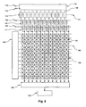
- the in Fig. 1 to 3 The image sensor shown can be used in both still and motion picture cameras, and has a plurality of photosensitive pixels 101 arranged in lines (shown horizontally here) and in columns (shown vertically here).
- the pixels 101 of each column are connected to a respective column line 103. All pixels of a row are connected to a respective row line 102.
- a row select circuit 104 allows the selection of a particular row line 102 so that all pixels of the respective row over the respective column lines 103 are connected to a respective signal preprocessor which in particular comprises column amplifiers.
- the signal preprocessing means present for each column line 103 are not shown individually here, but are part of a signal preprocessing unit 105, which in addition may also comprise sample-hold elements and / or analog-to-digital converters for digitizing the signals generated by the column amplifiers.
- the column lines 103 can each be connected via first switches 110 to a first test signal line 106.
- the column lines 103 can each be connected via second switches 111 to a second test signal line 107.
- Test input signals can be applied to the column lines 103 via the first test signal line 106 and the second test signal line 107.
- the signal pre-processing means of the signal preprocessing unit 105 are adapted to process not only the electrical signals (i.e., the wanted signals) generated by the pixels 101 and connected to the respective column line 103, but also the said test input signals.
- the three embodiments differ essentially by the control of the switches 110, 111, which will be explained in more detail below.
- the signal preprocessing unit 105 has a common output of the signal preprocessing devices, to which an evaluation unit 120 for the evaluation of the test input signals is connected.
- a first control line 108 for jointly controlling the first switches 110 and a second control line 109 for jointly controlling the second switches 111 are provided.
- a control signal to apply the test signals, either the first or the second control line 108 or 109 is supplied with a control signal.
- a first voltage source is applied to the first test signal line 106 and a second voltage source is applied to the second test signal line 107.
- the voltage sources may be both internal voltage sources integrated on the image sensor and external voltage sources.
- the first voltage source supplies a voltage of 2 V and the second voltage source supplies a voltage of 1.5 V.
- the regulation of the voltage sources must be designed so that the test voltages are stable and low-noise even under load.
- the first switches 110 are actuated, so that now the first voltage source with a voltage of 2 V is applied to the column lines 103. Subsequently, the image sensor is read so that the voltage of 2 V is read as a reference value in the respective signal preprocessing and buffered.
- connection of the column line 103 is interrupted with the first test signal line and by actuation of the second switch 111 by means of the second control line 109 connects to the second voltage source (1.5 V).
- This voltage is read into the respective signal preprocessing devices as a signal value and buffered.
- the voltage of 2 V corresponds to a reference value and the voltage of 1.5 V corresponds to a signal value.
- a test difference signal corresponding to the difference (0.5 V) of the two test input signals is produced at the output of the respective signal processing device (for example after amplification).
- the test difference signals generated in the individual signal preprocessing devices are digitized and output to the evaluation unit 120.
- a first test image can be generated, which corresponds to a bright input image.
- This first test image can be analyzed by the evaluation unit 120. For example, the digitized test difference signals can be compared with a predetermined reference value.
- the procedure described above is repeated, except that the first test voltage of 2 V is used for both the generation of the reference value and the signal value, that is, in the first passage.
- the column lines 103 are connected to the first test signal line 106 via the first switches 110. Due to the difference formation, the test difference signal in this case is 0 V, which is likewise digitized and output to the evaluation unit 120.
- the thus generated second test pattern corresponds to a black input image. This second test image can be analyzed separately in the evaluation unit 120 or compared with the first test image.
- test images By a line by line different control of the switches 110, 111 can be generated test images, which have horizontal lines.
- the 2V applied to the first test signal line 106 is used for both the reference value and the signal value, a test image is formed where every tenth line is bright, while all nine lines in between are dark.
- the second embodiment ( Fig. 2 ) differs from the first embodiment ( Fig. 1 ) in that the first and second switches 110, 111 are not driven via common control lines 108, 109, but that it can be separately selected for each column whether the associated column line 103 is to be connected to the first test signal line 106 or the second test signal line 107 , With others Words is the image sensor according to Fig. 2 adapted to considerablyrier the test input signals column by column variable on the column lines 103, ie without fixed pre-assignment, for example, due to a corresponding interconnection of associated transistors.
- a register 115 with a data input 113 is provided, via which data patterns can be loaded into the register 115.
- the size of the register 115 is determined by the column and row number of the image sensor.
- the data pattern stored in register 115 defines which of the two test signal lines 106, 107 should be connected to a specific column line 103.
- the register 115 thus serves as a control register.
- the register 115 has a number of register outputs 116 corresponding to the number of columns, the respective state of which can be determined by the data pattern and which are connected to a respective control logic 112.
- the control logics 112 are connected to a common control line 117. If a signal is present at this common control line 117, each control logic 112 actuates either a first switch 110 or a second switch 111 depending on the state of the associated register output 116.
- the register 115 also has a clock input 114, so that a different line of the data pattern is used to control the register outputs 116 for each test image line.
- corresponding data patterns in addition to test patterns with vertical stripe patterns, it is also possible to produce rectangular patterns or any other patterns.
- a register 115 can be used, which is designed only for storing single-line data patterns. After reading one or more lines with a particular data pattern, another data pattern can be loaded into the register 115 via the data input 113 so that test images with horizontal and vertical structures can also be generated with a single-line register.
- the third embodiment ( Fig. 3 ) largely corresponds to the second embodiment ( Fig. 2 ) and differs in that the control logics 112 are connected to two control lines 108, 109 instead of the common control line 117.
- Control line 108 Control line 109 Test signal line connected to the column lines 103: 0 0 no test signal line 1 0 first test signal line 106 0 1 second test signal line 107 1 1 Test signal line according to data pattern
- the feeding of the test voltages from the central test signal lines 106, 107 ensures in all embodiments that all column lines 103 connected to a respective test signal line 106, 107 are supplied with exactly the same test voltage. This avoids artifacts compared to solutions in which test signals are generated individually for each column and thus slightly differ from each other despite nominally the same voltage due to component tolerances.
- the switches 110, 111 ensure a direct, largely voltage-free and noise-free feeding of the test voltages into the column lines 103.
- a continuous monitoring of the image sensor in particular during regular operation of the camera can be done if one or two test images are generated in the manner described above between the reading of two useful signal images.
- the pixels of the image sensor can be deactivated.
- an automated evaluation of the test image (s) for the detection of defects or image defects can then take place, for example by an analysis by means of suitable methods on the basis of a Fourier analysis or a comparison with stored reference images.
- an optical or acoustic signal can be output to the operator of the camera.
Landscapes
- Engineering & Computer Science (AREA)
- Multimedia (AREA)
- Signal Processing (AREA)
- Health & Medical Sciences (AREA)
- Biomedical Technology (AREA)
- General Health & Medical Sciences (AREA)
- Transforming Light Signals Into Electric Signals (AREA)
Claims (13)
- Capteur d'image, en particulier capteur d'image CMOS, pour caméras électroniques, comprenant une pluralité de pixels photosensibles (101) agencés en rangées et en colonnes, dans lequel tous les pixels ou au moins une partie des pixels (101) d'une colonne sont reliés à une ligne de colonne commune respective (103), le capteur d'image comprenant, pour une ou pour plusieurs des lignes de colonnes (103), un système de prétraitement de signal (100) respectif afin de traiter les signaux utiles engendrés par les pixels et injectés sur la ligne de colonne respective (103), ledit capteur d'image étant réalisé pour injecter sur les lignes de colonnes (103) au choix un parmi au moins deux signaux d'entrée de test, et le capteur d'image comprenant au moins une première et une seconde source de tension pour générer les signaux d'entrée de test,
caractérisé en ce que
la source de tension respective est une source de tension régulée indépendamment de la tension d'alimentation du capteur d'image. - Capteur d'image selon la revendication 1,
caractérisé en ce que le capteur d'image est réalisé pour injecter les signaux d'entrée de test sans chute de tension sur les lignes de colonnes (103). - Capteur d'image selon la revendication 1 ou 2,
caractérisé en ce que chaque ligne de colonne (103) est reliée à au moins un premier commutateur respectif (110) et à un second commutateur respectif (111) de telle façon que la ligne de colonne respective (103) peut être reliée, via le premier commutateur (110) et le second commutateur (111), au choix avec une première ligne de signal de test (106) ou une seconde ligne de signal de test (107). - Capteur d'image selon la revendication 3,
caractérisé en ce que les premiers commutateurs (110) sont prévus entre la première ligne de signal de test (106) et la ligne de colonne respective (103), et en ce que les seconds commutateurs (111) sont prévus entre la seconde ligne de signal de test (107) et la ligne de colonne respective (103). - Capteur d'image selon la revendication 3 ou 4,
caractérisé en ce que les premiers commutateurs (110) sont reliés à une première ligne de commande (108) pour le pilotage commun des premiers commutateurs (110), et
en ce que les seconds commutateurs (111) sont reliés à une seconde ligne de commande (109) pour le pilotage commun des seconds commutateurs (111). - Capteur d'image selon la revendication 3 ou 4,
caractérisé en ce qu'il est prévu un registre (115) qui est réalisé pour piloter séparément les premiers et les seconds commutateurs (110, 111) pour chaque ligne de colonne (103), de sorte que la ligne de colonne respective (103) est reliée au choix avec la première ligne de signal de test (106), avec la seconde ligne de signal de test (107) ou avec aucune ligne de signal de test. - Capteur d'image selon la revendication 6,
caractérisé en ce qu'il est prévu une logique de commande respective (112) entre le registre (115) et le premier et le second commutateur (110, 111), les logiques de commande (112) étant reliées du côté entrée avec une sortie de registre respective (116) et avec une ligne de commande commune (117), et dans lequel les logiques de commande (112) sont réalisées pour actionner, en fonction d'un signal de commande sur la ligne de commande commune (117) soit le premier commutateur respectif (110) soit le second commutateur respectif (111) en fonction de la situation de la sortie de registre respective (116),
ou bien en ce qu'il est prévu une logique de commande respective (112) entre le registre (115) et le premier et le second commutateur (110, 111) de chaque ligne de colonne (103), les logiques de commande (112) étant reliées du côté entrée avec une sortie de registre respective (116) et avec une première ligne de commande commune (108) et avec une seconde ligne de commande commune (109), et dans lequel les logiques de commande (112) sont réalisées pour actionner, en fonction des signaux de commande sur la première ligne de commande (108) et sur la seconde ligne de commande (109) soit le premier commutateur respectif (110) soit le second commutateur respectif (111) en fonction de la situation de la sortie de registre respective (116) ou pour actionner la totalité des premiers commutateurs (110) ou la totalité des seconds commutateurs (111) indépendamment de la situation de la sortie de registre respective (116). - Capteur d'image selon l'une des revendications 3 à 7,
caractérisé en ce que les commutateurs (110, 111) sont intégrés dans le capteur d'image. - Capteur d'image selon l'une des revendications 3 à 8,
caractérisé en ce que la première source de tension est reliée ou susceptible d'être reliée à la première ligne de signal de test (106) et la seconde source de tension est reliée ou susceptible d'être reliée à la seconde ligne de signal de test (107). - Capteur d'image selon l'une des revendications précédentes,
caractérisé en ce que les lignes de colonne (103) sont susceptibles d'être reliées à différentes lignes de signal de test (106, 107),
et/ou en ce que les lignes de colonne (103) peuvent être alimentées par rangées avec différents signaux d'entrée de test. - Capteur d'image selon l'une des revendications précédentes,
caractérisé en ce que les systèmes de prétraitement de signaux (105) sont réalisés pour traiter également les signaux d'entrée de test appliqués aux lignes de colonne (103),
et/ou en ce que le système de prétraitement de signal respectif (105) comprend au moins un amplificateur de colonne et/ou un circuit d'échantillonnage-maintien,
et/ou en ce que le capteur d'image (103) comprend au moins un système d'évaluation (120) qui est relié à une sortie des systèmes de prétraitement de signaux (105), le système d'évaluation (120) étant réalisé pour évaluer les signaux d'entrée de test après leur traitement dans les systèmes de prétraitement de signaux (105). - Unité formant capteur d'image pour caméras électroniques, comprenant un capteur d'image qui comprend une pluralité de pixels photosensibles (101) agencés en rangées et en colonnes, dans laquelle tous les pixels ou au moins une partie des pixels (101) d'une colonne sont reliés à une ligne de colonne commune respective (103), le capteur d'image comprenant un système de prétraitement de signal (105) respectif pour une ou plusieurs des lignes de colonne (103), afin de traiter les signaux utiles engendrés par les pixels et injectés sur la ligne de colonne respective (103), et dans laquelle le capteur d'image est réalisé pour commuter au choix un parmi au moins deux signaux d'entrée de test sur les lignes de colonne (103),
caractérisée en ce que
l'unité formant capteur d'image comprend en outre au moins une première source de tension et une seconde source de tension pour engendrer les signaux d'entrée de test précités, lesdites sources de tension étant reliées à des bornes associées du capteur d'images, et dans laquelle la source de tension respective est une source de tension régulée indépendamment de la tension d'alimentation du capteur d'image. - Unité formant capteur d'image selon la revendication 12,
caractérisée en ce que chaque ligne de colonne (103) du capteur d'image est reliée à au moins un premier commutateur respectif (110) et à au moins un second commutateur respectif (111) de telle façon que la ligne de colonne respective (103) peut être reliée via le premier commutateur (110) et le second commutateur (111) au choix avec au moins une première ligne de signal de test (106) ou une seconde ligne de signal de test (107), et en ce que la première source de tension est reliée ou susceptible d'être reliée à la première ligne de signal de test (106) et la seconde source de tension est reliée ou susceptible d'être reliée à la seconde ligne de signal de test (107).
Applications Claiming Priority (1)
| Application Number | Priority Date | Filing Date | Title |
|---|---|---|---|
| DE102009049201A DE102009049201A1 (de) | 2009-10-13 | 2009-10-13 | Bildsensor und Betriebsverfahren |
Publications (2)
| Publication Number | Publication Date |
|---|---|
| EP2312864A1 EP2312864A1 (fr) | 2011-04-20 |
| EP2312864B1 true EP2312864B1 (fr) | 2012-09-19 |
Family
ID=43333037
Family Applications (1)
| Application Number | Title | Priority Date | Filing Date |
|---|---|---|---|
| EP10013479A Active EP2312864B1 (fr) | 2009-10-13 | 2010-10-08 | Capteur d'images et procédé de fonctionnement |
Country Status (3)
| Country | Link |
|---|---|
| US (1) | US8531566B2 (fr) |
| EP (1) | EP2312864B1 (fr) |
| DE (1) | DE102009049201A1 (fr) |
Families Citing this family (7)
| Publication number | Priority date | Publication date | Assignee | Title |
|---|---|---|---|---|
| US8921855B2 (en) * | 2011-03-09 | 2014-12-30 | Canon Kabushiki Kaisha | Test circuit for testing signal receiving unit, image pickup apparatus, method of testing signal receiving unit, and method of testing image pickup apparatus |
| US9052497B2 (en) | 2011-03-10 | 2015-06-09 | King Abdulaziz City For Science And Technology | Computing imaging data using intensity correlation interferometry |
| US9099214B2 (en) | 2011-04-19 | 2015-08-04 | King Abdulaziz City For Science And Technology | Controlling microparticles through a light field having controllable intensity and periodicity of maxima thereof |
| US8953047B2 (en) * | 2012-05-02 | 2015-02-10 | Aptina Imaging Corporation | Imaging systems with signal chain verification circuitry |
| US9584800B2 (en) * | 2014-03-31 | 2017-02-28 | Semiconductor Components Industries, Llc | Imaging systems with pixel array verification circuitry |
| RU2673454C1 (ru) * | 2018-01-23 | 2018-11-27 | Вячеслав Михайлович Смелков | Устройство "кольцевого" фотоприёмника для панорамного телевизионно-компьютерного сканирования монохромного изображения |
| EP4037308B1 (fr) | 2021-01-29 | 2024-07-31 | Stmicroelectronics (Grenoble 2) Sas | Capteurs d'images |
Family Cites Families (9)
| Publication number | Priority date | Publication date | Assignee | Title |
|---|---|---|---|---|
| US4843473A (en) * | 1988-03-21 | 1989-06-27 | Polaroid Corporation | Charge injection device with low noise readout |
| GB8921561D0 (en) | 1989-09-23 | 1989-11-08 | Univ Edinburgh | Designs and procedures for testing integrated circuits containing sensor arrays |
| US5654537A (en) | 1995-06-30 | 1997-08-05 | Symbios Logic Inc. | Image sensor array with picture element sensor testability |
| US6504572B2 (en) | 1997-11-05 | 2003-01-07 | Stmicroelectronics, Inc. | Circuit for detecting leaky access switches in CMOS imager pixels |
| US6366312B1 (en) * | 1998-06-09 | 2002-04-02 | Intel Corporation | Testing components in digital imaging devices |
| US6734897B1 (en) * | 1999-08-10 | 2004-05-11 | Agilent Technologies, Inc | Digital imaging circuit and method |
| US6797933B1 (en) | 2001-06-29 | 2004-09-28 | Vanguard International Semiconductor Corporation | On-chip design-for-testing structure for CMOS APS (active pixel sensor) image sensor |
| US7714266B2 (en) * | 2007-01-12 | 2010-05-11 | Aptina Imaging Corporation | Method and apparatus for measuring source follower gain in an image sensor array |
| DE102009004409A1 (de) | 2009-01-13 | 2010-07-15 | Arnold & Richter Cine Technik Gmbh & Co. Betriebs Kg | Bildsensor |
-
2009
- 2009-10-13 DE DE102009049201A patent/DE102009049201A1/de not_active Withdrawn
-
2010
- 2010-10-07 US US12/900,115 patent/US8531566B2/en active Active
- 2010-10-08 EP EP10013479A patent/EP2312864B1/fr active Active
Also Published As
| Publication number | Publication date |
|---|---|
| US8531566B2 (en) | 2013-09-10 |
| EP2312864A1 (fr) | 2011-04-20 |
| US20110242375A1 (en) | 2011-10-06 |
| DE102009049201A1 (de) | 2011-04-28 |
Similar Documents
| Publication | Publication Date | Title |
|---|---|---|
| EP2312864B1 (fr) | Capteur d'images et procédé de fonctionnement | |
| DE3632487C2 (fr) | ||
| DE3248928C2 (fr) | ||
| DE2902134A1 (de) | Fehlerkompensiervorrichtung fuer einen festkoerper-bildabnehmer | |
| DE3687242T2 (de) | Bildeingangsvorrichtung und verfahren zur korrektur ihrer eingangssignale. | |
| DE69427051T2 (de) | Photoelektrische Umwandlungsanordnung | |
| DE2648641B2 (de) | Elektronische Anordnung zum Lesen von Zeichen | |
| DE69215323T2 (de) | Schwarzabgleichseinstellung für mit mehreren Festkörper-Bildaufnahmevorrichtungen versehene Videokameras | |
| DE3604964C2 (fr) | ||
| DE102016203392B3 (de) | Bildinspektionsverfahren mit mehreren Kameras | |
| EP0365786B1 (fr) | Méthode de détermination de la fonction de transfert d'une caméra vidéo | |
| DE3501572C2 (de) | Verfahren zum Detektieren von Bildinformation bezüglich einer fotografischen Abbildung | |
| DE3889337T2 (de) | Bildlesevorrichtung. | |
| DE3620525A1 (de) | Verfahren und vorrichtung zur spektrografischen messung der dichte eines farbnegativfilms | |
| DE10216806B4 (de) | Verfahren und Vorrichtung zur FPN-Korrektur von Bildsignalwerten eines Bildsensors | |
| DE19926129A1 (de) | Verfahren und Vorrichtung zum Testen von Photoempfängerarrays und von zugeordneten Lesekanälen | |
| DE3030140A1 (de) | Verfahren zur optischen ueberpruefung von stabfoermigen gegenstaenden und einrichtung zur durchfuehrung des verfahrens | |
| DE19543488A1 (de) | Verfahren und Vorrichtung zur Bildwert-Korrektur bei optoelektronischen Wandlern | |
| DE69621312T2 (de) | Bildeingabegerät | |
| DE3309949C2 (fr) | ||
| DE10121811A1 (de) | Fehlererkennung und -korrektur in Referenzstreifen für die Kalibrierung von Scannvorrichtungen | |
| DE68918984T2 (de) | Bildeingangsapparat. | |
| EP1537652B1 (fr) | Ensemble photodetecteur et procede de compensation de lumiere parasite | |
| EP0342318A1 (fr) | Ajustement automatique de la netteté pour tubes images | |
| DE102005010986B4 (de) | Verfahren und Vorrichtung zum Aufnehmen eines Wärmebildes |
Legal Events
| Date | Code | Title | Description |
|---|---|---|---|
| PUAI | Public reference made under article 153(3) epc to a published international application that has entered the european phase |
Free format text: ORIGINAL CODE: 0009012 |
|
| AK | Designated contracting states |
Kind code of ref document: A1 Designated state(s): AL AT BE BG CH CY CZ DE DK EE ES FI FR GB GR HR HU IE IS IT LI LT LU LV MC MK MT NL NO PL PT RO RS SE SI SK SM TR |
|
| AX | Request for extension of the european patent |
Extension state: BA ME |
|
| 17P | Request for examination filed |
Effective date: 20111020 |
|
| GRAP | Despatch of communication of intention to grant a patent |
Free format text: ORIGINAL CODE: EPIDOSNIGR1 |
|
| GRAS | Grant fee paid |
Free format text: ORIGINAL CODE: EPIDOSNIGR3 |
|
| GRAA | (expected) grant |
Free format text: ORIGINAL CODE: 0009210 |
|
| AK | Designated contracting states |
Kind code of ref document: B1 Designated state(s): AL AT BE BG CH CY CZ DE DK EE ES FI FR GB GR HR HU IE IS IT LI LT LU LV MC MK MT NL NO PL PT RO RS SE SI SK SM TR |
|
| REG | Reference to a national code |
Ref country code: GB Ref legal event code: FG4D Free format text: NOT ENGLISH |
|
| REG | Reference to a national code |
Ref country code: CH Ref legal event code: EP |
|
| REG | Reference to a national code |
Ref country code: IE Ref legal event code: FG4D Free format text: LANGUAGE OF EP DOCUMENT: GERMAN |
|
| REG | Reference to a national code |
Ref country code: AT Ref legal event code: REF Ref document number: 576515 Country of ref document: AT Kind code of ref document: T Effective date: 20121015 |
|
| REG | Reference to a national code |
Ref country code: DE Ref legal event code: R096 Ref document number: 502010001275 Country of ref document: DE Effective date: 20121115 |
|
| PG25 | Lapsed in a contracting state [announced via postgrant information from national office to epo] |
Ref country code: HR Free format text: LAPSE BECAUSE OF FAILURE TO SUBMIT A TRANSLATION OF THE DESCRIPTION OR TO PAY THE FEE WITHIN THE PRESCRIBED TIME-LIMIT Effective date: 20120919 Ref country code: FI Free format text: LAPSE BECAUSE OF FAILURE TO SUBMIT A TRANSLATION OF THE DESCRIPTION OR TO PAY THE FEE WITHIN THE PRESCRIBED TIME-LIMIT Effective date: 20120919 Ref country code: NO Free format text: LAPSE BECAUSE OF FAILURE TO SUBMIT A TRANSLATION OF THE DESCRIPTION OR TO PAY THE FEE WITHIN THE PRESCRIBED TIME-LIMIT Effective date: 20121219 Ref country code: LT Free format text: LAPSE BECAUSE OF FAILURE TO SUBMIT A TRANSLATION OF THE DESCRIPTION OR TO PAY THE FEE WITHIN THE PRESCRIBED TIME-LIMIT Effective date: 20120919 |
|
| REG | Reference to a national code |
Ref country code: NL Ref legal event code: VDEP Effective date: 20120919 |
|
| REG | Reference to a national code |
Ref country code: LT Ref legal event code: MG4D Effective date: 20120919 |
|
| PG25 | Lapsed in a contracting state [announced via postgrant information from national office to epo] |
Ref country code: GR Free format text: LAPSE BECAUSE OF FAILURE TO SUBMIT A TRANSLATION OF THE DESCRIPTION OR TO PAY THE FEE WITHIN THE PRESCRIBED TIME-LIMIT Effective date: 20121220 Ref country code: SI Free format text: LAPSE BECAUSE OF FAILURE TO SUBMIT A TRANSLATION OF THE DESCRIPTION OR TO PAY THE FEE WITHIN THE PRESCRIBED TIME-LIMIT Effective date: 20120919 Ref country code: SE Free format text: LAPSE BECAUSE OF FAILURE TO SUBMIT A TRANSLATION OF THE DESCRIPTION OR TO PAY THE FEE WITHIN THE PRESCRIBED TIME-LIMIT Effective date: 20120919 Ref country code: LV Free format text: LAPSE BECAUSE OF FAILURE TO SUBMIT A TRANSLATION OF THE DESCRIPTION OR TO PAY THE FEE WITHIN THE PRESCRIBED TIME-LIMIT Effective date: 20120919 |
|
| BERE | Be: lapsed |
Owner name: ARNOLD&RICHTER CINE TECHNIK GMBH&CO. BETRIEBS K.G. Effective date: 20121031 |
|
| PG25 | Lapsed in a contracting state [announced via postgrant information from national office to epo] |
Ref country code: ES Free format text: LAPSE BECAUSE OF FAILURE TO SUBMIT A TRANSLATION OF THE DESCRIPTION OR TO PAY THE FEE WITHIN THE PRESCRIBED TIME-LIMIT Effective date: 20121230 Ref country code: RO Free format text: LAPSE BECAUSE OF FAILURE TO SUBMIT A TRANSLATION OF THE DESCRIPTION OR TO PAY THE FEE WITHIN THE PRESCRIBED TIME-LIMIT Effective date: 20120919 Ref country code: NL Free format text: LAPSE BECAUSE OF FAILURE TO SUBMIT A TRANSLATION OF THE DESCRIPTION OR TO PAY THE FEE WITHIN THE PRESCRIBED TIME-LIMIT Effective date: 20120919 Ref country code: EE Free format text: LAPSE BECAUSE OF FAILURE TO SUBMIT A TRANSLATION OF THE DESCRIPTION OR TO PAY THE FEE WITHIN THE PRESCRIBED TIME-LIMIT Effective date: 20120919 Ref country code: CZ Free format text: LAPSE BECAUSE OF FAILURE TO SUBMIT A TRANSLATION OF THE DESCRIPTION OR TO PAY THE FEE WITHIN THE PRESCRIBED TIME-LIMIT Effective date: 20120919 Ref country code: IS Free format text: LAPSE BECAUSE OF FAILURE TO SUBMIT A TRANSLATION OF THE DESCRIPTION OR TO PAY THE FEE WITHIN THE PRESCRIBED TIME-LIMIT Effective date: 20130119 |
|
| PG25 | Lapsed in a contracting state [announced via postgrant information from national office to epo] |
Ref country code: PT Free format text: LAPSE BECAUSE OF FAILURE TO SUBMIT A TRANSLATION OF THE DESCRIPTION OR TO PAY THE FEE WITHIN THE PRESCRIBED TIME-LIMIT Effective date: 20130121 Ref country code: MC Free format text: LAPSE BECAUSE OF NON-PAYMENT OF DUE FEES Effective date: 20121031 Ref country code: SK Free format text: LAPSE BECAUSE OF FAILURE TO SUBMIT A TRANSLATION OF THE DESCRIPTION OR TO PAY THE FEE WITHIN THE PRESCRIBED TIME-LIMIT Effective date: 20120919 Ref country code: PL Free format text: LAPSE BECAUSE OF FAILURE TO SUBMIT A TRANSLATION OF THE DESCRIPTION OR TO PAY THE FEE WITHIN THE PRESCRIBED TIME-LIMIT Effective date: 20120919 |
|
| REG | Reference to a national code |
Ref country code: IE Ref legal event code: MM4A |
|
| PLBE | No opposition filed within time limit |
Free format text: ORIGINAL CODE: 0009261 |
|
| REG | Reference to a national code |
Ref country code: FR Ref legal event code: ST Effective date: 20130628 |
|
| STAA | Information on the status of an ep patent application or granted ep patent |
Free format text: STATUS: NO OPPOSITION FILED WITHIN TIME LIMIT |
|
| PG25 | Lapsed in a contracting state [announced via postgrant information from national office to epo] |
Ref country code: DK Free format text: LAPSE BECAUSE OF FAILURE TO SUBMIT A TRANSLATION OF THE DESCRIPTION OR TO PAY THE FEE WITHIN THE PRESCRIBED TIME-LIMIT Effective date: 20120919 Ref country code: BE Free format text: LAPSE BECAUSE OF NON-PAYMENT OF DUE FEES Effective date: 20121031 Ref country code: RS Free format text: LAPSE BECAUSE OF FAILURE TO SUBMIT A TRANSLATION OF THE DESCRIPTION OR TO PAY THE FEE WITHIN THE PRESCRIBED TIME-LIMIT Effective date: 20120919 Ref country code: IE Free format text: LAPSE BECAUSE OF NON-PAYMENT OF DUE FEES Effective date: 20121008 Ref country code: BG Free format text: LAPSE BECAUSE OF FAILURE TO SUBMIT A TRANSLATION OF THE DESCRIPTION OR TO PAY THE FEE WITHIN THE PRESCRIBED TIME-LIMIT Effective date: 20121219 |
|
| 26N | No opposition filed |
Effective date: 20130620 |
|
| PG25 | Lapsed in a contracting state [announced via postgrant information from national office to epo] |
Ref country code: IT Free format text: LAPSE BECAUSE OF FAILURE TO SUBMIT A TRANSLATION OF THE DESCRIPTION OR TO PAY THE FEE WITHIN THE PRESCRIBED TIME-LIMIT Effective date: 20120919 Ref country code: FR Free format text: LAPSE BECAUSE OF NON-PAYMENT OF DUE FEES Effective date: 20121119 |
|
| REG | Reference to a national code |
Ref country code: DE Ref legal event code: R097 Ref document number: 502010001275 Country of ref document: DE Effective date: 20130620 |
|
| PG25 | Lapsed in a contracting state [announced via postgrant information from national office to epo] |
Ref country code: AL Free format text: LAPSE BECAUSE OF FAILURE TO SUBMIT A TRANSLATION OF THE DESCRIPTION OR TO PAY THE FEE WITHIN THE PRESCRIBED TIME-LIMIT Effective date: 20120919 Ref country code: CY Free format text: LAPSE BECAUSE OF FAILURE TO SUBMIT A TRANSLATION OF THE DESCRIPTION OR TO PAY THE FEE WITHIN THE PRESCRIBED TIME-LIMIT Effective date: 20120919 Ref country code: MT Free format text: LAPSE BECAUSE OF FAILURE TO SUBMIT A TRANSLATION OF THE DESCRIPTION OR TO PAY THE FEE WITHIN THE PRESCRIBED TIME-LIMIT Effective date: 20120919 |
|
| PG25 | Lapsed in a contracting state [announced via postgrant information from national office to epo] |
Ref country code: TR Free format text: LAPSE BECAUSE OF FAILURE TO SUBMIT A TRANSLATION OF THE DESCRIPTION OR TO PAY THE FEE WITHIN THE PRESCRIBED TIME-LIMIT Effective date: 20120919 |
|
| PG25 | Lapsed in a contracting state [announced via postgrant information from national office to epo] |
Ref country code: SM Free format text: LAPSE BECAUSE OF FAILURE TO SUBMIT A TRANSLATION OF THE DESCRIPTION OR TO PAY THE FEE WITHIN THE PRESCRIBED TIME-LIMIT Effective date: 20120919 Ref country code: LU Free format text: LAPSE BECAUSE OF NON-PAYMENT OF DUE FEES Effective date: 20121008 |
|
| PG25 | Lapsed in a contracting state [announced via postgrant information from national office to epo] |
Ref country code: HU Free format text: LAPSE BECAUSE OF FAILURE TO SUBMIT A TRANSLATION OF THE DESCRIPTION OR TO PAY THE FEE WITHIN THE PRESCRIBED TIME-LIMIT Effective date: 20101008 |
|
| REG | Reference to a national code |
Ref country code: CH Ref legal event code: PL |
|
| PG25 | Lapsed in a contracting state [announced via postgrant information from national office to epo] |
Ref country code: MK Free format text: LAPSE BECAUSE OF FAILURE TO SUBMIT A TRANSLATION OF THE DESCRIPTION OR TO PAY THE FEE WITHIN THE PRESCRIBED TIME-LIMIT Effective date: 20120919 Ref country code: CH Free format text: LAPSE BECAUSE OF NON-PAYMENT OF DUE FEES Effective date: 20141031 Ref country code: LI Free format text: LAPSE BECAUSE OF NON-PAYMENT OF DUE FEES Effective date: 20141031 |
|
| REG | Reference to a national code |
Ref country code: AT Ref legal event code: MM01 Ref document number: 576515 Country of ref document: AT Kind code of ref document: T Effective date: 20151008 |
|
| PG25 | Lapsed in a contracting state [announced via postgrant information from national office to epo] |
Ref country code: AT Free format text: LAPSE BECAUSE OF NON-PAYMENT OF DUE FEES Effective date: 20151008 |
|
| PGFP | Annual fee paid to national office [announced via postgrant information from national office to epo] |
Ref country code: DE Payment date: 20251020 Year of fee payment: 16 |
|
| PGFP | Annual fee paid to national office [announced via postgrant information from national office to epo] |
Ref country code: GB Payment date: 20251024 Year of fee payment: 16 |