EP2317515A2 - Phasenerkennungsschaltung für einen Taktwiederherstellungskreis - Google Patents
Phasenerkennungsschaltung für einen Taktwiederherstellungskreis Download PDFInfo
- Publication number
- EP2317515A2 EP2317515A2 EP10188947A EP10188947A EP2317515A2 EP 2317515 A2 EP2317515 A2 EP 2317515A2 EP 10188947 A EP10188947 A EP 10188947A EP 10188947 A EP10188947 A EP 10188947A EP 2317515 A2 EP2317515 A2 EP 2317515A2
- Authority
- EP
- European Patent Office
- Prior art keywords
- values
- signal
- generate
- soft
- bit
- Prior art date
- Legal status (The legal status is an assumption and is not a legal conclusion. Google has not performed a legal analysis and makes no representation as to the accuracy of the status listed.)
- Withdrawn
Links
Images


Classifications
-
- G—PHYSICS
- G11—INFORMATION STORAGE
- G11B—INFORMATION STORAGE BASED ON RELATIVE MOVEMENT BETWEEN RECORD CARRIER AND TRANSDUCER
- G11B20/00—Signal processing not specific to the method of recording or reproducing; Circuits therefor
- G11B20/10—Digital recording or reproducing
- G11B20/10009—Improvement or modification of read or write signals
-
- G—PHYSICS
- G11—INFORMATION STORAGE
- G11B—INFORMATION STORAGE BASED ON RELATIVE MOVEMENT BETWEEN RECORD CARRIER AND TRANSDUCER
- G11B20/00—Signal processing not specific to the method of recording or reproducing; Circuits therefor
- G11B20/10—Digital recording or reproducing
- G11B20/10009—Improvement or modification of read or write signals
- G11B20/10037—A/D conversion, D/A conversion, sampling, slicing and digital quantisation or adjusting parameters thereof
-
- G—PHYSICS
- G11—INFORMATION STORAGE
- G11B—INFORMATION STORAGE BASED ON RELATIVE MOVEMENT BETWEEN RECORD CARRIER AND TRANSDUCER
- G11B20/00—Signal processing not specific to the method of recording or reproducing; Circuits therefor
- G11B20/10—Digital recording or reproducing
- G11B20/10009—Improvement or modification of read or write signals
- G11B20/10046—Improvement or modification of read or write signals filtering or equalising, e.g. setting the tap weights of an FIR filter
- G11B20/10055—Improvement or modification of read or write signals filtering or equalising, e.g. setting the tap weights of an FIR filter using partial response filtering when writing the signal to the medium or reading it therefrom
-
- G—PHYSICS
- G11—INFORMATION STORAGE
- G11B—INFORMATION STORAGE BASED ON RELATIVE MOVEMENT BETWEEN RECORD CARRIER AND TRANSDUCER
- G11B20/00—Signal processing not specific to the method of recording or reproducing; Circuits therefor
- G11B20/10—Digital recording or reproducing
- G11B20/10009—Improvement or modification of read or write signals
- G11B20/10222—Improvement or modification of read or write signals clock-related aspects, e.g. phase or frequency adjustment or bit synchronisation
-
- G—PHYSICS
- G11—INFORMATION STORAGE
- G11B—INFORMATION STORAGE BASED ON RELATIVE MOVEMENT BETWEEN RECORD CARRIER AND TRANSDUCER
- G11B20/00—Signal processing not specific to the method of recording or reproducing; Circuits therefor
- G11B20/10—Digital recording or reproducing
- G11B20/10009—Improvement or modification of read or write signals
- G11B20/10268—Improvement or modification of read or write signals bit detection or demodulation methods
- G11B20/10287—Improvement or modification of read or write signals bit detection or demodulation methods using probabilistic methods, e.g. maximum likelihood detectors
- G11B20/10296—Improvement or modification of read or write signals bit detection or demodulation methods using probabilistic methods, e.g. maximum likelihood detectors using the Viterbi algorithm
-
- H—ELECTRICITY
- H03—ELECTRONIC CIRCUITRY
- H03L—AUTOMATIC CONTROL, STARTING, SYNCHRONISATION OR STABILISATION OF GENERATORS OF ELECTRONIC OSCILLATIONS OR PULSES
- H03L7/00—Automatic control of frequency or phase; Synchronisation
- H03L7/06—Automatic control of frequency or phase; Synchronisation using a reference signal applied to a frequency- or phase-locked loop
- H03L7/07—Automatic control of frequency or phase; Synchronisation using a reference signal applied to a frequency- or phase-locked loop using several loops, e.g. for redundant clock signal generation
-
- H—ELECTRICITY
- H03—ELECTRONIC CIRCUITRY
- H03L—AUTOMATIC CONTROL, STARTING, SYNCHRONISATION OR STABILISATION OF GENERATORS OF ELECTRONIC OSCILLATIONS OR PULSES
- H03L7/00—Automatic control of frequency or phase; Synchronisation
- H03L7/06—Automatic control of frequency or phase; Synchronisation using a reference signal applied to a frequency- or phase-locked loop
- H03L7/08—Details of the phase-locked loop
- H03L7/0807—Details of the phase-locked loop concerning mainly a recovery circuit for the reference signal
-
- H—ELECTRICITY
- H03—ELECTRONIC CIRCUITRY
- H03L—AUTOMATIC CONTROL, STARTING, SYNCHRONISATION OR STABILISATION OF GENERATORS OF ELECTRONIC OSCILLATIONS OR PULSES
- H03L7/00—Automatic control of frequency or phase; Synchronisation
- H03L7/06—Automatic control of frequency or phase; Synchronisation using a reference signal applied to a frequency- or phase-locked loop
- H03L7/08—Details of the phase-locked loop
- H03L7/081—Details of the phase-locked loop provided with an additional controlled phase shifter
- H03L7/0812—Details of the phase-locked loop provided with an additional controlled phase shifter and where no voltage or current controlled oscillator is used
-
- H—ELECTRICITY
- H03—ELECTRONIC CIRCUITRY
- H03L—AUTOMATIC CONTROL, STARTING, SYNCHRONISATION OR STABILISATION OF GENERATORS OF ELECTRONIC OSCILLATIONS OR PULSES
- H03L7/00—Automatic control of frequency or phase; Synchronisation
- H03L7/06—Automatic control of frequency or phase; Synchronisation using a reference signal applied to a frequency- or phase-locked loop
- H03L7/08—Details of the phase-locked loop
- H03L7/085—Details of the phase-locked loop concerning mainly the frequency- or phase-detection arrangement including the filtering or amplification of its output signal
- H03L7/091—Details of the phase-locked loop concerning mainly the frequency- or phase-detection arrangement including the filtering or amplification of its output signal the phase or frequency detector using a sampling device
-
- H—ELECTRICITY
- H03—ELECTRONIC CIRCUITRY
- H03M—CODING; DECODING; CODE CONVERSION IN GENERAL
- H03M1/00—Analogue/digital conversion; Digital/analogue conversion
- H03M1/12—Analogue/digital converters
- H03M1/124—Sampling or signal conditioning arrangements specially adapted for A/D converters
- H03M1/1245—Details of sampling arrangements or methods
- H03M1/1255—Synchronisation of the sampling frequency or phase to the input frequency or phase
-
- H—ELECTRICITY
- H04—ELECTRIC COMMUNICATION TECHNIQUE
- H04L—TRANSMISSION OF DIGITAL INFORMATION, e.g. TELEGRAPHIC COMMUNICATION
- H04L7/00—Arrangements for synchronising receiver with transmitter
- H04L7/0054—Detection of the synchronisation error by features other than the received signal transition
-
- G—PHYSICS
- G11—INFORMATION STORAGE
- G11B—INFORMATION STORAGE BASED ON RELATIVE MOVEMENT BETWEEN RECORD CARRIER AND TRANSDUCER
- G11B2220/00—Record carriers by type
- G11B2220/20—Disc-shaped record carriers
- G11B2220/25—Disc-shaped record carriers characterised in that the disc is based on a specific recording technology
- G11B2220/2508—Magnetic discs
- G11B2220/2516—Hard disks
Definitions
- the disclosed subject matter is directed to signal processing and, in particular, to phase detection in timing recovery loops.
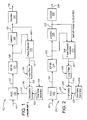
- Fig. 1 is a block diagram of a prior-art read channel 100 for a hard drive.
- Read channel 100 receives an analog input signal 121 corresponding to data stored on the hard drive and generates a digital decoded output signal 129 representing the data stored on the hard drive.
- analog-to-digital converter (ADC) 122 digitizes analog input signal 121 to generate digital input signal 123.
- Digital finite impulse response (DFIR) filter equalizer 124 equalizes digital input signal 123 to generate equalized digital signal 125.
- Soft detector 126 converts equalized digital signal 125 into soft values, such as multi-bit log likelihood ratio (LLR) values 127, where each LLR value has a hard-decision sign bit and a multi-bit (e.g., 4-bit) confidence value.
- Soft detector 126 implements a suitable detection technique, such as Viterbi soft-output detection or maximum a posteriori (MAP) detection, to generate LLR values 127.
- Decoder 128 decodes the LLR values to generate decoded output signal 129. For example, if the data stored on the hard drive is encoded using a low-density parity check (LDPC) code, then decoder 128 performs LDPC decoding to generate decoded output signal 129 from LLR values
- Phase detector 130 processes equalized digital signal 125 from equalizer 124 and the sign bits of LLR values 127 from soft detector 126 to generate an estimated timing error signal 131.
- phase detector 130 generates estimated timing error signal 131 by (i) convolving the sign bits with a finite impulse response (FIR) filter, (ii) generating the difference between the FIR filter output and a one-cycle-delayed version of equalized digital signal 125, and (iii) multiplying that difference by an estimate of the slope of equalized digital signal 125.
- Loop filter 132 integrates estimated timing error signal 131 to output an averaged error signal 133.
- Time-base generator e.g., local oscillator (LO)
- Interpolator 136 shifts the phase of LO clock signal 135 based on averaged error signal 133 to generate sampling clock signal 137, which determines the timing of the sampling of analog input signal 121 by ADC 122.
- the signal-to-noise ratio continues to decrease due to increasing storage density of the disks.
- Conventional timing-recovery phase detectors that estimate timing information from equalized samples (such as equalized digital signal 125) and hard decisions (such as the sign bits of LLR values 127) might not operate properly in low-SNR environments, resulting in an unacceptably high loss-of-lock rate (LOLR), which reduces system throughput.
- LOLR loss-of-lock rate
- phase detector 130 may output timing error signals that result in relatively high loss-of-lock rates and relatively low system throughput.
- the disclosed subject matter addresses the problems of the contemporary art by providing a mechanism for graduated or "soft" changes in the Non Return Zeros (NRZs) and used to adjust the sampling clock signal for the ADC of the disclosed subject matter, as opposed to relatively large or “hard” changes of NRZs in the prior art.
- NRZs Non Return Zeros
- the disclosed phase detector utilizes the sign bit and one or more and possibly all of the remaining confidence-value bits, in producing the estimated timing error signal.
- the confidence values allow the phase detector to treat different sign bits differently in producing the estimated timing error signal, where the confidence value provides reliability information for the received sign bit. For example, low confidence values for the sign bit may cause the phase detector to reduce the impact of the sign bit, while high confidence values may cause larger changes in the estimated timing error signals.
- phase changes are detected with greater accuracy and reliability than with the prior-art phase detectors. Potentially large and sudden phase changes in the sampling clock signal of the prior art are replaced by smoother and more gradual "soft" phase changes with the disclosed system. This results in sampling clock signals that allow for gradual or “soft” adjustments in the ADC. Additionally, the disclosed phase detector performs its operations dynamically and “on the fly,” without having to stop and readjust the interpolator.
- the present invention is a signal processor.
- the signal processor comprises, a signal processing path that converts an analog input signal into a digital output signal, wherein the signal processing path generates multi-bit soft values, each multi-bit soft value having a sign bit and a multi-bit confidence value; and, a timing recovery loop that uses the sign bits and one or more bits of the multi-bit confidence values of the soft values to generate a sampling clock signal used by the signal processing path to sample the analog input signal.
- the present invention is a method for signal processing.
- the method comprises converting an analog input signal into multi-bit soft values, each multi-bit soft value having a sign bit and a multi-bit confidence value; and, using the sign bits and one or more bits of the multi-bit confidence values of the soft values to generate a sampling clock signal to sample the analog input signal.
- Fig. 1 is a block diagram of a prior-art read channel for a hard drive
- Fig. 2 is a block diagram of a read channel for a hard drive of the disclosed subject matter
- Fig. 3 is a block diagram of the phase detector of the read channel of Fig. 2 ;
- Phase detector 230 utilizes the confidence value to determine the reliability of the sign bit and generates an estimated timing error signal that is more accurate when compared to using only the sign bit of the input LLR value. As opposed to the "all or nothing" operation of phase detector 130 of Fig. 1 , phase detector 230 is known as a "soft" phase detector. LLR values having numbers of bits other than five are possible in other implementations of read channel 200.
- PR targets having other tap coefficients, values, and/or other numbers of taps can be used.
- Each filtered value 309 is subjected to a one-clock-cycle delay in delay mechanism 310, with the resultant delayed signal 309' received by multiplier 304b. Filtered signal 309 is also sent directly (i.e., without delay) to multiplier 304a.
- Fig. 5 is a graphical representation of the performance of read channel 200 of Fig. 2 versus prior-art read channel 100 of Fig. 1 .
- Fig. 5 shows the loss-of-lock rate (LOLR) for each read channel as a function of signal-to-noise ratio (SNR), where the results for prior-art read channel 100 are indicated by squares, and the results for read channel 200 are indicated by circles.
- SNR signal-to-noise ratio
- read channel 200 provides about an order of magnitude improvement in LOLR compared to prior-art read channel 100.
Landscapes
- Engineering & Computer Science (AREA)
- Signal Processing (AREA)
- Computer Networks & Wireless Communication (AREA)
- Theoretical Computer Science (AREA)
- Physics & Mathematics (AREA)
- Probability & Statistics with Applications (AREA)
- Synchronisation In Digital Transmission Systems (AREA)
- Digital Transmission Methods That Use Modulated Carrier Waves (AREA)
- Signal Processing For Digital Recording And Reproducing (AREA)
Applications Claiming Priority (1)
| Application Number | Priority Date | Filing Date | Title |
|---|---|---|---|
| US12/609,031 US7974369B2 (en) | 2009-10-30 | 2009-10-30 | Phase detector for timing recovery loop |
Publications (2)
| Publication Number | Publication Date |
|---|---|
| EP2317515A2 true EP2317515A2 (de) | 2011-05-04 |
| EP2317515A3 EP2317515A3 (de) | 2011-05-25 |
Family
ID=43522378
Family Applications (1)
| Application Number | Title | Priority Date | Filing Date |
|---|---|---|---|
| EP10188947A Withdrawn EP2317515A3 (de) | 2009-10-30 | 2010-10-26 | Phasenerkennungsschaltung für einen Taktwiederherstellungskreis |
Country Status (6)
| Country | Link |
|---|---|
| US (1) | US7974369B2 (de) |
| EP (1) | EP2317515A3 (de) |
| JP (1) | JP5330319B2 (de) |
| KR (1) | KR101378007B1 (de) |
| CN (1) | CN102055471B (de) |
| TW (1) | TWI420878B (de) |
Families Citing this family (18)
| Publication number | Priority date | Publication date | Assignee | Title |
|---|---|---|---|---|
| US8281224B1 (en) * | 2008-10-20 | 2012-10-02 | Link—A—Media Devices Corporation | Programmable LBA and dummy bit reliabilities |
| US8429500B2 (en) * | 2010-03-31 | 2013-04-23 | Lsi Corporation | Methods and apparatus for computing a probability value of a received value in communication or storage systems |
| US8149529B2 (en) * | 2010-07-28 | 2012-04-03 | Lsi Corporation | Dibit extraction for estimation of channel parameters |
| US9135106B2 (en) * | 2012-05-22 | 2015-09-15 | Hgst Technologies Santa Ana, Inc. | Read level adjustment using soft information |
| US8848308B2 (en) * | 2013-03-04 | 2014-09-30 | Lsi Corporation | Systems and methods for ADC sample based inter-track interference compensation |
| US9281006B2 (en) | 2013-12-13 | 2016-03-08 | Avago Technologies General Ip (Singapore) Pte. Ltd. | Systems and methods for ATI characterization |
| US8917467B1 (en) | 2013-12-13 | 2014-12-23 | Lsi Corporation | Systems and methods for ATI mitigation |
| US9083366B1 (en) | 2014-03-12 | 2015-07-14 | Avago Technologies General Ip (Singapore) Pte. Ltd. | Alignment of sampling phases in a multi-channel time-interleaved analog-to-digital converter |
| US9240199B2 (en) | 2014-03-12 | 2016-01-19 | Avago Technologies General Ip (Singapore) Pte. Ltd. | Systems and methods for distortion characterization |
| US9099157B1 (en) | 2014-04-22 | 2015-08-04 | Avago Technologies General Ip (Singapore) Pte. Ltd. | Systems and methods for adjacent track interference based re-writing |
| US9350526B2 (en) * | 2014-10-27 | 2016-05-24 | The United States Of America As Represented By The Secretary Of The Air Force | Non-integer oversampled timing recovery for higher order quadrature modulation communication systems using in-phase samples |
| US9319217B1 (en) * | 2014-10-28 | 2016-04-19 | The United States Of America As Represented By The Secretary Of The Air Force | Non-integer oversampled timing recovery for higher order quadrature modulation communication systems using quadrature-phase samples |
| US10277256B2 (en) * | 2016-01-05 | 2019-04-30 | Mediatek Inc. | Decoding across transmission time intervals |
| US9882710B2 (en) * | 2016-06-23 | 2018-01-30 | Macom Connectivity Solutions, Llc | Resolving interaction between channel estimation and timing recovery |
| US9641185B1 (en) * | 2016-06-30 | 2017-05-02 | Intel IP Corporation | Digital time converter systems and method |
| US10135606B2 (en) | 2016-10-27 | 2018-11-20 | Macom Connectivity Solutions, Llc | Mitigating interaction between adaptive equalization and timing recovery |
| US10050774B1 (en) * | 2017-05-02 | 2018-08-14 | MACOM Technology Solutions Holding, Inc. | Mitigating interaction between adaptive equalization and timing recovery |
| US11979163B2 (en) * | 2022-10-03 | 2024-05-07 | Western Digital Technologies, Inc. | Oversampled phase lock loop in a read channel |
Family Cites Families (10)
| Publication number | Priority date | Publication date | Assignee | Title |
|---|---|---|---|---|
| DE4308000B4 (de) * | 1993-03-13 | 2006-11-30 | Robert Bosch Gmbh | Verfahren zur entscheidungsrückgekoppelten Taktableitung |
| JP3428339B2 (ja) * | 1996-12-11 | 2003-07-22 | 日本ビクター株式会社 | 位相同期制御回路 |
| EP1234420A2 (de) * | 1999-12-03 | 2002-08-28 | Broadcom Corporation | Viterbi-slicer für turbokoden |
| EP1187344B1 (de) * | 2000-08-28 | 2005-11-23 | Sony Deutschland Gmbh | Soft-Normalisierer für einen Kanaldekoder |
| JP3749889B2 (ja) * | 2002-10-17 | 2006-03-01 | 株式会社東芝 | Prml検出を適用する信号処理デバイス、同デバイスを備えたディスク記憶装置、及び同装置におけるフィードバック制御のための信号処理方法 |
| US7239682B2 (en) * | 2002-11-12 | 2007-07-03 | Carnegie Mellon University | Timing recovery system and method |
| US20080212708A1 (en) * | 2004-02-19 | 2008-09-04 | Thomson Licensing | Method and Apparatus for Carrier Recovery in a Communications System |
| US7653155B1 (en) * | 2004-11-04 | 2010-01-26 | Sandia Corporation | Using convolutional decoding to improve time delay and phase estimation in digital communications |
| EP2031791A1 (de) * | 2007-08-30 | 2009-03-04 | Deutsche Thomson OHG | Vorrichtung und Verfahren zum Wiederherstellen von Daten aus einem getakteten Eingabesignal |
| TWI358204B (en) * | 2007-12-12 | 2012-02-11 | Ind Tech Res Inst | All digital phase lock loop and method for control |
-
2009
- 2009-10-30 US US12/609,031 patent/US7974369B2/en active Active
-
2010
- 2010-05-27 TW TW099117070A patent/TWI420878B/zh not_active IP Right Cessation
- 2010-06-08 JP JP2010130632A patent/JP5330319B2/ja not_active Expired - Fee Related
- 2010-06-18 CN CN201010208283.0A patent/CN102055471B/zh active Active
- 2010-06-25 KR KR1020100060412A patent/KR101378007B1/ko not_active Expired - Fee Related
- 2010-10-26 EP EP10188947A patent/EP2317515A3/de not_active Withdrawn
Non-Patent Citations (1)
| Title |
|---|
| None |
Also Published As
| Publication number | Publication date |
|---|---|
| US20110103527A1 (en) | 2011-05-05 |
| KR101378007B1 (ko) | 2014-03-27 |
| CN102055471B (zh) | 2015-05-20 |
| JP5330319B2 (ja) | 2013-10-30 |
| EP2317515A3 (de) | 2011-05-25 |
| US7974369B2 (en) | 2011-07-05 |
| CN102055471A (zh) | 2011-05-11 |
| KR20110047961A (ko) | 2011-05-09 |
| TW201116022A (en) | 2011-05-01 |
| JP2011097559A (ja) | 2011-05-12 |
| TWI420878B (zh) | 2013-12-21 |
Similar Documents
| Publication | Publication Date | Title |
|---|---|---|
| US7974369B2 (en) | Phase detector for timing recovery loop | |
| US8312359B2 (en) | Branch-metric calibration using varying bandwidth values | |
| US8018360B2 (en) | Systems and methods for mitigating latency in a data detector feedback loop | |
| EP2562756A2 (de) | Lesekanal mit überabgetasteter Analog-Digital-Wandlung | |
| TWI310637B (en) | Digital signal processor, receiver, corrector and methods for the same | |
| US20120124454A1 (en) | Systems and Methods for ADC Sample Based Timing Recovery | |
| TW589622B (en) | PRML system with branch estimation | |
| US8874633B2 (en) | Determining coefficients for digital low pass filter given cutoff and boost values for corresponding analog version | |
| US20130050005A1 (en) | Read Channel With Oversampled Analog To Digital Conversion And Parallel Data Detectors | |
| US8422609B2 (en) | Automatic filter-reset mechanism | |
| US8610608B2 (en) | Systems and methods for reduced latency loop correction | |
| US8760991B2 (en) | Systems and methods for post processing gain correction | |
| US20060023780A1 (en) | Equaliser circuit | |
| US20140198405A1 (en) | Systems and Methods for Loop Processing With Variance Adaptation | |
| US8976471B1 (en) | Systems and methods for two stage tone reduction | |
| CN100382190C (zh) | 具有分支估测器的部分响应最大可能性系统 | |
| JP4575226B2 (ja) | 適応等化器 | |
| JP5099035B2 (ja) | デジタルフィルタ | |
| JP2001332033A (ja) | 位相比較器およびこれを用いる同期信号生成回路 |
Legal Events
| Date | Code | Title | Description |
|---|---|---|---|
| PUAI | Public reference made under article 153(3) epc to a published international application that has entered the european phase |
Free format text: ORIGINAL CODE: 0009012 |
|
| PUAL | Search report despatched |
Free format text: ORIGINAL CODE: 0009013 |
|
| AK | Designated contracting states |
Kind code of ref document: A2 Designated state(s): AL AT BE BG CH CY CZ DE DK EE ES FI FR GB GR HR HU IE IS IT LI LT LU LV MC MK MT NL NO PL PT RO RS SE SI SK SM TR |
|
| AX | Request for extension of the european patent |
Extension state: BA ME |
|
| AK | Designated contracting states |
Kind code of ref document: A3 Designated state(s): AL AT BE BG CH CY CZ DE DK EE ES FI FR GB GR HR HU IE IS IT LI LT LU LV MC MK MT NL NO PL PT RO RS SE SI SK SM TR |
|
| AX | Request for extension of the european patent |
Extension state: BA ME |
|
| RIC1 | Information provided on ipc code assigned before grant |
Ipc: H03L 7/091 20060101ALI20110418BHEP Ipc: H03L 7/081 20060101ALI20110418BHEP Ipc: H03M 1/12 20060101ALI20110418BHEP Ipc: G11B 20/10 20060101AFI20110207BHEP |
|
| 17P | Request for examination filed |
Effective date: 20111124 |
|
| STAA | Information on the status of an ep patent application or granted ep patent |
Free format text: STATUS: THE APPLICATION HAS BEEN WITHDRAWN |
|
| 18W | Application withdrawn |
Effective date: 20160727 |