EP2317672B1 - Justiereinrichtung der zeitverzögerung und verfahren dafür - Google Patents
Justiereinrichtung der zeitverzögerung und verfahren dafür Download PDFInfo
- Publication number
- EP2317672B1 EP2317672B1 EP09771936.3A EP09771936A EP2317672B1 EP 2317672 B1 EP2317672 B1 EP 2317672B1 EP 09771936 A EP09771936 A EP 09771936A EP 2317672 B1 EP2317672 B1 EP 2317672B1
- Authority
- EP
- European Patent Office
- Prior art keywords
- signal
- digital
- signals
- delayer
- inserter
- Prior art date
- Legal status (The legal status is an assumption and is not a legal conclusion. Google has not performed a legal analysis and makes no representation as to the accuracy of the status listed.)
- Active
Links
Images




Classifications
-
- H—ELECTRICITY
- H04—ELECTRIC COMMUNICATION TECHNIQUE
- H04B—TRANSMISSION
- H04B10/00—Transmission systems employing electromagnetic waves other than radio-waves, e.g. infrared, visible or ultraviolet light, or employing corpuscular radiation, e.g. quantum communication
- H04B10/50—Transmitters
- H04B10/501—Structural aspects
- H04B10/503—Laser transmitters
- H04B10/505—Laser transmitters using external modulation
-
- H—ELECTRICITY
- H04—ELECTRIC COMMUNICATION TECHNIQUE
- H04B—TRANSMISSION
- H04B10/00—Transmission systems employing electromagnetic waves other than radio-waves, e.g. infrared, visible or ultraviolet light, or employing corpuscular radiation, e.g. quantum communication
- H04B10/50—Transmitters
- H04B10/58—Compensation for non-linear transmitter output
Definitions
- the present invention relates to signal processing, and more particularly to a time delay adjustment technology.
- dispersion refers to waveform distortion of signals caused by different frequency components of the transmitted signal or different transmission speeds of various mode components of signals.
- the main influence on optical transmission caused by dispersion is intersymbol interference generated between data pulses, and the damage on the system performance caused by dispersion usually cannot be ignored. Therefore, an optical fiber transmission system having a transmission speed higher than 10Gbits/s generally needs a dispersion compensation technology to ensure a transmission function of the system.
- Electronics dispersion compensation specially electronic dispersion pre-compensation (electronic pre distortion, EPD) performed at an originating, has long-distance dispersion compensation capability. As shown in FIG.
- a digital signal processor sends two signals, the two signals are multiplexed by a multiplexer, the multiplexed signals are converted by a digital-to-analog converter into analog signals, and the analog signals are amplified by an amplifier, so that two signals I and Q are modulated onto a light signal sent by a light source for transmission.
- DSP digital signal processor
- FIG. 2 shows another EPD system in the prior art, in which a phase shifter is connected before the multiplexer to change the delay difference between the two signals I and Q by changing phases.
- the US Patent Application Pub. No.2006/0078336 discloses that optical dispersion imposed on a communications signal conveyed through an optical communications system is compensated by modulating the communications signal in the electrical domain. A compensation function is determined that substantially mitigates the chromatic dispersion. The communications signal is then modulated in the electrical domain using the compensation function.
- compensation is implemented in the transmitter, using a look-up-table and digital-to-analog converter to generate an electrical predistorted signal. The electrical predistorted signal is then used to modulate an optical source to generate a corresponding predistorted optical signal for transmission through the optical communications system.
- the document UK Patent Application GB 2397388 aims to provide an optical transmitter utilizing an external Mach-Zehnder type optical modulator serially connected to an optical phase modulator.
- the optical modulator is capable of optimizing an optical wavelength chirp to be added to a transmission optical signal.
- a Mach-Zehnder optical modulator comprises an input, output and first and second arms.
- An optical phase modulator receives light from output and transmits the light along waveguide.
- the optical transmitter also includes amplitude adjusting means, phase adjusting means, amplitude controlling means and phase controlling means. All of which are used to control the drive signal applied to the optical phase modulator.
- the US Patent Application Pub. No.2004/071438 discloses a method for introducing errors into a digital fiber optic communication link so that small analog changes in optical transmission efficiency can be determined by changes in the audible error rate.
- the method comprises providing a transmitter with a test channel that provides a pseudorandom encoded optical transmission through coupled fiber optic cables.
- the signal is sent through the cables and received by a receiver which introduces and measures errors.
- the received signal is split and processed by a clock recovery circuit and a lowpass filter.
- the clock recovery circuit obtains the optimal sampling point.
- the lowpass filter filters the data and provides a timing adjustment relative to the recovered clock signal.
- the clock retimes the filtered data with a sampling comparator.
- the variable timing introduces errors allowing optical transmission efficiency measurements.
- a bit error rate tester produces audible sounds whose frequency content is related to the bit error rate.
- Optimal transmission efficiency is determined by manipulating the cables and their associated ferrules until the audible sounds have the lowest frequencies.
- a transmit path correction system for compensating for I/Q gain imbalances and I/Q phase imbalances includes a mixed signal feed forward path and a mixed signal feedback path.
- the mixed signal feed forward path includes a digital DC offset correction circuit for compensating for digital DC offsets in the mixed signal feed forward path using a feedback signal, an I/Q phase equalization circuit for compensating for the I/Q phase imbalances in the mixed signal feed forward path, and an I/Q gain equalization circuit for compensating for the I/Q gain imbalances in the mixed signal feed forward path using the feedback signal.
- the mixed signal feedback path processes the output of the mixed signal feed forward path to produce the feedback signal.
- the delay difference may be processed in an offline state (that is, when the delay difference is adjusted, no service can be transmitted), the operation is complicated, and real-time monitoring and adjustment of the delay cannot be achieved.
- the present invention provides a time delay adjustment device, which includes a first signal inserter, a first delayer, a first power splitter, a first filter, a second signal inserter, a second power splitter, a second filter, and a controller.
- the first signal inserter is configured to receive a first signal, and insert a scrambling signal into the first signal.
- the first delayer is configured to delay the signal processed by the first signal inserter.
- the first power splitter is configured to extract a part of signal from the signal delayed by the first delayer.
- the first filter is configured to filter the signal extracted by the first power splitter, and output the scrambling signal inserted by the first signal inserter.
- the second signal inserter is configured to receive a second signal, and insert a scrambling signal into the second signal.
- the inserted scrambling signal is the same as that inserted by the first signal inserter.
- the second power splitter is configured to extract a part of signal from the signal output by the second signal inserter.
- the second filter is configured to filter the signal extracted by the second power splitter, and output the scrambling signal inserted by the second signal inserter.
- the controller is configured to receive signals sent by the first filter and the second filter, detect a delay difference between the two signals according to a difference between the two signals, and change the delay difference between the two signals by adjusting a delay of the first delayer.
- the present invention provides an optical transmission apparatus, which includes in its first implementation form a digital signal processor, a time delay adjustment device, a light source, and a modulator.
- the digital signal processor is configured to transmit a first digital signal and a second digital signal.
- the time delay adjustment device is configured to adjust a delay difference between the first digital signal and the second digital signal during transmission of the signals.
- the light source is configured to generate a light signal.
- the modulator is configured to modulate two signals adjusted by the time delay adjustment device onto the light signal, and send the modulated light signal.
- the time delay adjustment device includes a first signal inserter, a first digital-to-analog converter, a first delayer, a first power splitter, a first filter, a second signal inserter, a second digital-to-analog converter, a second power splitter, a second filter, and a controller.
- the first signal inserter is configured to receive a first digital signal, and insert a scrambling signal into the first digital signal.
- the first digital-to-analog converter is configured to convert the signal processed by the first signal inserter into an analog signal.
- the first delayer is configured to delay the analog signal converted by the first digital-to-analog converter.
- the first power splitter is connected to the modulator and the first delayer, and configured to extract a part of signal from the signal delayed by the first delayer.
- the first filter is configured to filter the signal extracted by the first power splitter, and output the scrambling signal inserted by the first signal inserter.
- the second signal inserter is configured to receive a second digital signal, and insert a scrambling signal into the second digital signal.
- the inserted scrambling signal is the same as that inserted by the first signal inserter.
- the second digital-to-analog converter is configured to convert the signal processed by the second signal inserter into an analog signal.
- the second power splitter is connected to the modulator and the second analog-to-digital converter, and configured to extract a part of signal from the signal converted by the second analog-to-digital converter.
- the second filter is configured to filter the signal extracted by the second power splitter, and output the scrambling signal inserted by the second signal inserter.
- the controller is configured to receive signals output by the first filter and the second filter, detect a delay difference between the two signals according to a difference between the two signals, and change the delay difference between the two signals by adjusting the first delayer.
- the present invention provides an optical transmission apparatus, which includes in its second implementation form a digital signal processor, a time delay adjustment device, a light source, and a modulator.
- the digital signal processor is configured to transmit a first digital signal and a second digital signal.
- the time delay adjustment device is configured to adjust a delay difference between the first digital signal and the second digital signal during transmission of the signals.
- the light source is configured to generate a light signal.
- the modulator is configured to modulate two signals adjusted by the time delay adjustment device onto the light signal, and send the modulated light signal.
- the time delay adjustment device includes a first signal inserter, a first delayer, a first digital-to-analog converter, a first power splitter, a first filter, a second signal inserter, a second digital-to-analog converter, a second power splitter, a second filter, and a controller.
- the first signal inserter is configured to receive a first digital signal, and insert a scrambling signal into the first digital signal.
- the first delayer is configured to delay the signal processed by the first signal inserter.
- the first digital-to-analog converter is configured to convert the signal processed by the first delayer into an analog signal.
- the first power splitter is connected to the modulator and the first analog-to-digital converter, and configured to extract a part of signal from the signal converted by the first analog-to-digital converter.
- the first filter is configured to filter the signal extracted by the first power splitter, and output the scrambling signal inserted by the first signal inserter.
- the second signal inserter is configured to receive a second digital signal, and insert a scrambling signal into the second digital signal.
- the inserted scrambling signal is the same as that inserted by the first signal inserter.
- the second digital-to-analog converter is configured to convert the signal processed by the second delayer into an analog signal.
- the second power splitter is connected to the modulator and the second analog-to-digital converter, and configured to extract a part of signal from the signal converted by the second analog-to-digital converter.
- the second filter is configured to filter the signal extracted by the second power splitter, and output the scrambling signal inserted by the second signal inserter.
- the controller is configured to receive signals output by the first filter and the second filter, detect a delay difference between the two signals according to a difference between the two signals, and change the delay difference between the two signals by adjusting the first delayer.
- the present invention provides a time delay adjustment method, which includes the following steps:
- a same scrambling signal is added into the two signals, and at least one of the two signals is delayed.
- the added scrambling signals are extracted from the two signals separately.
- a delay difference between the two signals is detected according to a difference between the two extracted scrambling signals, and the delay difference between the two signals is adjusted by delaying at least one of the two signals.
- the delay difference is detected by detecting the inserted scrambling signals, the delay is adjusted by using a controller, so that on-line adjustment of delay time for the optical transmission apparatus is achieved, the operation is simple and quick, and moreover, real-time monitoring and adjustment of delay difference is also achieved.
- a time delay adjustment device includes a controller and two groups of a signal inserter, a delayer, a power splitter, and a filter that are connected in sequence.
- a first signal inserter is configured to receive a first signal and insert a scrambling signal into the signal.
- the scrambling signal is, for example, a single frequency scrambling A 1 sin( ⁇ 1 t), or multiple single frequency scrambling A 1 sin( ⁇ 1 t)+A 2 sin( ⁇ 2 t)+... +A n sin( ⁇ n t), in which the n is a natural number, and the A n and ⁇ n are rational numbers.
- a first delayer is configured to delay the signal processed by the first signal inserter.
- a first power splitter is configured to extract a part of (for example, 5%) signal from the signal delayed by the first delayer.
- a first filter is configured to filter the signal extracted by the first power splitter, and output the scrambling signal inserted by the first signal inserter.
- a second signal inserter is configured to receive a second signal, and insert a scrambling signal into the signal.
- the inserted scrambling signal is the same as that inserted by the first signal inserter.
- a second delayer is configured to delay the signal processed by the second signal inserter.
- a second power splitter is configured to extract a part of (for example, 5%) signal from the signal delayed by the second delayer.
- a second filter is configured to filter the signal extracted by the second power splitter, and output the scrambling signal inserted by the second signal inserter.
- the controller is connected to the first delayer, the second delayer, the first filter, and the second filter, is configured to receive signals output by the first filter and the second filter, detect a delay difference by calculating an amplitude of a difference between the two signals, and control the delay difference between the two signals by delaying the first delayer and/or the second delayer.
- the controller may be connected to the first signal inserter and the second signal inserter, and control the scrambling signal corresponding to the first signal inserter and the second signal inserter.
- the filter outputs a signal with a frequency of ⁇ 1 and the two signals are subtracted to obtain the following formula: 2 ⁇ A 1 ⁇ sin ⁇ 1 ⁇ ⁇ / 2 ⁇ cos ⁇ 1 ⁇ t - ⁇ / 2
- the scrambling signal is A 1 sin( ⁇ 1 t)+A 2 sin( ⁇ 2 t)+...+A n sin( ⁇ n t)
- the difference is that the two signals are subtracted to obtain 2A 1 sin( ⁇ 1 ⁇ /2)cos ⁇ 1 (t- ⁇ /2)+ 2A 2 sin( ⁇ 2 ⁇ /2)cos ⁇ 2 (t- ⁇ /2)+... +2A n sin( ⁇ n ⁇ /2)cos ⁇ n (t- ⁇ /2).
- the filter has more options and may select a signal at a certain frequency for filtering.
- the filter filters a signal at a certain frequency, and formula (3) changes into 2 ⁇ A n ⁇ sin ⁇ n ⁇ ⁇ / 2 ⁇ cos ⁇ n ⁇ t - ⁇ / 2
- the signal may be extended by using the Fourier series, while the Fourier function is formed by sine functions.
- the Fourier function is formed by sine functions.
- a square wave is superimposition of multiple sine waves, which also falls within the scope of the embodiments of the present invention.
- the first signal inserter and the second signal inserter only need to have signal insertion functions, for example, an amplifier or offset T.
- first digital-to-analog converter and a second digital-to-analog converter may be added.
- the first digital-to-analog converter is disposed between the first signal inserter and the first delayer or between the first delayer and the first power splitter and configured to perform digital-to-analog conversion on the signal before the first signal inserter sends the signal to the first delayer or before the first delayer sends the signal to the first power splitter.
- the second digital-to-analog converter is disposed between the second signal inserter and the second delayer or between the second delayer and the second power splitter and configured to perform digital-to-analog conversion on the signal before the second signal inserter sends the signal to the second delayer or before the second delayer sends the signal to the second power splitter.
- FIG 4 shows another time delay adjustment device according to the first embodiment, in which the first digital-to-analog converter is disposed between the first signal inverter and the first delayer and the second digital-to-analog converter is disposed between the second signal inserter and the second delayer.
- the situations in which the first digital-to-analog converter and the second digital-to-analog converter are disposed at other positions are not shown in FIG. 4 .
- the first filter and the second filter only need to have a function of outputting a signal at a certain frequency, for example, a bandpass filter, a high-pass filter, and a low-pass filter.
- on-line delay adjustment can be achieved, the operation is simple and delay adjustment is rapid, and real-time monitoring and adjustment of delay difference is also achieved.
- multiple-single-frequency scrambling serves as a scrambling signal, as multiple frequencies are optional, the reliability is improved.
- this embodiment is substantially the same as the first embodiment.
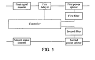
- the difference between the second embodiment and the first embodiment is that in the second embodiment, only one delayer exists and the controller adjusts the first delayer to adjust the delay difference between the two signals.
- the delayer may cause a certain delay on the signal
- the two signals are subjected to the influence of the delayers.
- the influence is the same, the delay on the two signals of the delayers are counteracted and may need to be considered.
- it is necessary to consider the delay of the first delayer.
- a delay of the first signal with respect to the second signal is ⁇ , and the first delayer may cause a delay ⁇ , so that the delay in total is ⁇ + ⁇ .
- FIG. 5 shows merely the situation in which no digital-to-analog converter exists, this is merely for ease of description.
- Persons skilled in the art should know that various situations in the first embodiment may also be used in the second embodiment. That is, a digital-to-analog converter may exist or may not exist.
- the same situation may also exist in other embodiments, for example, in a third embodiment, only a first delayer exists.
- the situations that are similar to this embodiment will not be described in the other embodiments.
- on-line delay adjustment can be achieved, the operation is simple, the delay adjustment is rapid, and real-time monitoring and adjustment of the delay difference is also achieved.
- multiple-single-frequency scrambling serves as a scrambling signal, multiple frequencies are optional, so that the reliability is improved. Compared with the first embodiment, the cost is reduced.
- a time delay adjustment method is provided, which is applied to the device in the first and second embodiments.
- the method includes the following steps. Two digital signals are received. A same scrambling signal is added into the two signals and at least one of the two signals is delayed. The added scrambling signals are extracted from the two signals. The delay difference between the two signals is detected according to the difference between the two scrambling signals and the delay difference between the two signals are adjusted by delaying at least one of the two signals.
- a signal with a frequency ⁇ 1 is extracted and the two signals are subtracted to obtain the following formula: 2 ⁇ A 1 ⁇ sin ⁇ 1 ⁇ ⁇ / 2 ⁇ cos ⁇ 1 ⁇ t - ⁇ / 2
- the scrambling signal is A 1 sin( ⁇ 1 t)+A 2 sin( ⁇ 2 t)+...+A n sin( ⁇ n t)
- the difference is that the two signals are subtracted to obtain 2A 1 sin( ⁇ 1 ⁇ /2)cos ⁇ 1 (t- ⁇ /2)+ 2A 2 sin( ⁇ 2 ⁇ /2)cos ⁇ 2 (t- ⁇ /2)+... +2A n sin( ⁇ n ⁇ /2)cos ⁇ n (t- ⁇ /2).
- the filter has many options, and may select a signal of a certain frequency for filtering.
- a signal at a certain frequency is filtered by the filter, and formula (3) changes to be: 2 ⁇ A n ⁇ sin ⁇ n ⁇ ⁇ / 2 ⁇ cos ⁇ n ⁇ t - ⁇ / 2
- the description of the method is omitted.
- the signal may be extended by using the Fourier series, while the Fourier function is formed by sine functions.
- a square wave is superimposition of multiple sine waves, which also falls within the scope of this embodiment of the present invention.
- Multiple-single-frequency scrambling is not essentially different from the previous method, the description of which is omitted here.
- the embodiment of the present invention needs to be repeated only to ensure the delay difference between all two signals, so that the delay difference between all the signals are ensured.
- the delay difference between B and C with respect to A is no higher than t 1 , the delay difference between the three signals A, B, and C are not greater than t 1 . Therefore, delay processing on three or more signals is applicable to the present invention is. For ease of description, the situation is no longer described in the other embodiments.
- on-line delay adjustment can be achieved, the operation is simple, delay adjustment is quick, and real-time monitoring and adjustment of the delay difference is also achieved.
- multiple-single-frequency scrambling serves as a scrambling signal, multiple frequencies are optional, so that the reliability is improved.
- an optical transmission apparatus for example, an electronic dispersion pre-compensation device, which includes a digital signal processor and a time delay adjustment device.
- the digital signal processor is configured to transmit a first digital signal, a second digital signal, a light source, and a modulator.
- the time delay adjustment device is configured to adjust a delay difference between the first digital signal and the second digital signal during transmission of the signals.
- the light source is configured to generate a light signal.
- the modulator is configured to modulate the two signals adjusted by the time delay adjustment device onto the light signal and send the modulated light signal.
- the time delay adjustment device includes a first signal inserter, a first digital-to-analog converter, a first delayer, a first power splitter, a first filter, a second signal inserter, a second digital-to-analog converter, a second delayer, a second power splitter, a second filter, and a controller.
- the first signal inserter is configured to receive the first digital signal and insert a scrambling signal into the first digital signal.
- the first digital-to-analog converter is configured to convert the signal processed by the first signal inserter into an analog signal.
- the first delayer is configured to delay the analog signal converted by the first digital-to-analog converter.
- the first power splitter is connected to the modulator and the first delayer and configured to extract a part of signal from the signal delayed by the first delayer.
- the first filter is configured to filter the signal extracted by the first power splitter and output the scrambling signal inserted by the first signal inserter.
- the second signal inserter is configured to receive the second digital signal and insert a scrambling signal into the first digital signal.
- the inserted scrambling signal is the same as the scrambling signal inserted by the first signal inserter.
- the second digital-to-analog converter is configured to convert the signal processed by the second signal inserter into an analog signal.
- the second delayer is configured to delay the analog signal converted by the second digital-to-analog converter.
- the second power splitter is connected to the modulator and the second delayer and configured to extract a part of signal from the signal delayed by the second delayer.
- the second filter is configured to filter the signal extracted by the second power splitter and output the scrambling signal inserted by the second signal inserter.
- the controller is configured to receive signals output by the first filter and the second filter, detect a delay difference between the two signals according to a difference between the two signals, and change the delay difference between the two signals by adjusting the first delayer and/or the second delayer.
- the electronic dispersion compensation device may no longer need an additional amplifier.
- the first signal inserter and the second signal inserter are other components such as an offset T and do not have enough amplification function, amplifiers are added between the two outputs of the time delay adjustment device and the modulator respectively.
- the optical transmission apparatus of this embodiment is characterized in that the time delay adjustment device is different from that in the prior art, and the time delay adjustment device and the method corresponding to the device, and various combinations and optional situations are described in detail in the previous embodiments (see the first, second, and third embodiments), which is no longer described here.
- on-line delay adjustment of the optical transmission apparatus can be achieved, the operation is simple, delay adjustment is rapid, and real-time monitoring and adjustment of delay difference is also achieved.
- multiple-single-frequency scrambling serves as a scrambling signal, multiple frequencies are optional, so that the reliability is improved.
Landscapes
- Physics & Mathematics (AREA)
- Electromagnetism (AREA)
- Engineering & Computer Science (AREA)
- Computer Networks & Wireless Communication (AREA)
- Signal Processing (AREA)
- Optics & Photonics (AREA)
- Nonlinear Science (AREA)
- Optical Communication System (AREA)
Claims (8)
- Zeitverzögerungs-Einstellungseinrichtung, umfassend:eine erste Signaleinfügungsvorrichtung, die dafür ausgelegt ist, ein erstes Signal zu empfangen und ein Verwürfelungssignal in das erste Signal einzufügen;eine erste Verzögerungsvorrichtung, die dafür ausgelegt ist, das durch die erste Signaleinfügungsvorrichtung verarbeitete Signal zu verzögern;einen ersten Leistungsteiler, der dafür ausgelegt ist, einen Teil des Signals von dem durch die erste Verzögerungsvorrichtung verzögerten Signals zu extrahieren;ein erstes Filter, das dafür ausgelegt ist, das durch den ersten Leistungsteiler extrahierte Signal zu filtern und das durch die erste Signaleinfügungsvorrichtung eingefügte Verwürfelungssignal auszugeben;eine zweite Signaleinfügungsvorrichtung, die dafür ausgelegt ist, ein zweites Signal zu empfangen und ein Verwürfelungssignal in das zweite Signal einzufügen, wobei das eingefügte Verwürfelungssignal dasselbe wie das durch die erste Signaleinfügungsvorrichtung eingefügte ist;einen zweiten Leistungsteiler, der dafür ausgelegt ist, einen Teil des Signals von dem durch die zweite Signaleinfügungsvorrichtung ausgegebenen Signal zu extrahieren;ein zweites Filter, das dafür ausgelegt ist, das durch den zweiten Leistungsteiler extrahierte Signal zu filtern und das durch die zweite Signaleinfügungsvorrichtung eingefügte Verwürfelungssignal auszugeben; undeine Steuerung, die dafür ausgelegt ist, durch das erste Filter und das zweite Filter gesendete Signale zu empfangen, eine Verzögerungsdifferenz zwischen den beiden Signalen gemäß einer Differenz zwischen den beiden Signalen zu detektieren und die Verzögerungsdifferenz zwischen den beiden Signalen durch Einstellen einer Verzögerung der ersten Verzögerungsvorrichtung zu ändern.
- Einrichtung nach Anspruch 1, ferner umfassend:eine zweite Verzögerungsvorrichtung, die dafür ausgelegt ist, das durch die zweite Signaleinfügungsvorrichtung verarbeitete Signal zu verzögern, wobei der zweite Leistungsteiler einen Teil des Signals von dem durch die zweite Verzögerungsvorrichtung verzögerten Signal extrahiert unddie Steuerung die Verzögerungsdifferenz zwischen den beiden Signalen gemäß der Differenz zwischen den durch das erste Filter und das zweite Filter gesendeten empfangenen Signalen detektiert und die Verzögerungsdifferenz zwischen den beiden Signalen durch Einstellen der Verzögerung der ersten Verzögerungsvorrichtung und/oder der zweiten Verzögerungsvorrichtung ändert.
- Einrichtung nach Anspruch 1 oder 2, die, wenn das erste Signal ein digitales Signal ist, ferner Folgendes umfasst:einen ersten Digital-Analog-Umsetzer, der zwischen der ersten Signaleinfügungsvorrichtung und der ersten Verzögerungsvorrichtung angeordnet und dafür ausgelegt ist, Digital-Analog-Umsetzung an einem Signal auszuführen, bevor die erste Signaleinfügungsvorrichtung das Signal zu der ersten Verzögerungsvorrichtung sendet; odereinen ersten Digital-Analog-Umsetzer, der zwischen der ersten Verzögerungsvorrichtung und dem ersten Leistungsteiler angeordnet und dafür ausgelegt ist, Digital-Analog-Umsetzung an dem Signal auszuführen, bevor die erste Verzögerungsvorrichtung das Signal zu dem ersten Leistungsteiler sendet; undwenn das zweite Signal ein digitales Signal ist, ferner Folgendes umfasst:einen zweiten Digital-Analog-Umsetzer, der zwischen der zweiten Signaleinfügungsvorrichtung und der zweiten Verzögerungsvorrichtung angeordnet und dafür ausgelegt ist, Digital-Analog-Umsetzung an dem Signal auszuführen,bevor die zweite Signaleinfügungsvorrichtung das Signal zu der zweiten Verzögerungsvorrichtung sendet; odereinen zweiten Digital-Analog-Umsetzer, der zwischen der zweiten Verzögerungsvorrichtung und dem zweiten Leistungsteiler angeordnet und dafür ausgelegt ist, Digital-Analog-Umsetzung an dem Signal auszuführen, bevor die zweite Verzögerungsvorrichtung das Signal zu dem zweiten Leistungsteiler sendet.
- Einrichtung nach Anspruch 1 oder 2, wobei
die Steuerung die Verzögerungsdifferenz zwischen den beiden Signalen gemäß einer Amplitude der Differenz zwischen den beiden Signalen detektiert. - Optische Übertragungsvorrichtung, umfassend:einen digitalen Signalprozessor, der dafür ausgelegt ist, ein erstes digitales Signal und ein zweites digitales Signal zu übertragen;eine Zeitverzögerungs-Einstellungseinrichtung, die dafür ausgelegt ist, eine Verzögerungsdifferenz zwischen dem ersten digitalen Signal und dem zweiten digitalen Signal während der Übertragung einzustellen;eine Lichtquelle, die dafür ausgelegt ist, ein Lichtsignal zu erzeugen;einen Modulator, der dafür ausgelegt ist, zwei durch die Zeitverzögerungs-Einstellungseinrichtung eingestellte Signale auf das Lichtsignal zu modulieren und das modulierte Lichtsignal zu senden;wobei die Zeitverzögerungs-Einstellungseinrichtung Folgendes umfasst:eine erste Signaleinfügungsvorrichtung, die dafür ausgelegt ist, ein erstes digitales Signal zu empfangen und ein Verwürfelungssignal in das erste digitale Signal einzufügen;einen ersten Digital-Analog-Umsetzer, der dafür ausgelegt ist, das durch die erste Signaleinfügungsvorrichtung verarbeitete Signal in ein analoges Signal umzusetzen;eine erste Verzögerungsvorrichtung, die dafür ausgelegt ist, das durch den ersten Digital-Analog-Umsetzer umgesetzte analoge Signal zu verzögern;einen ersten Leistungsteiler, der mit dem Modulator und der ersten Verzögerungsvorrichtung verbunden und dafür ausgelegt ist, einen Teil des Signals von dem durch die erste Verzögerungsvorrichtung verzögerten Signal zu extrahieren;ein erstes Filter, das dafür ausgelegt ist, das durch den ersten Leistungsteiler extrahierte Signal zu filtern und das durch die erste Signaleinfügungsvorrichtung eingefügte Verwürfelungssignal auszugeben;eine zweite Signaleinfügungsvorrichtung, die dafür ausgelegt ist, ein zweites digitales Signal zu empfangen und ein Verwürfelungssignal in das zweite digitale Signal einzufügen, wobei das eingefügte Verwürfelungssignal dasselbe wie das durch die erste Signaleinfügungsvorrichtung eingefügte ist;einen zweiten Digital-Analog-Umsetzer, der dafür ausgelegt ist, das durch die zweite Signaleinfügungsvorrichtung verarbeitete Signal in ein analoges Signal umzusetzen;einen zweiten Leistungsteiler, der mit dem Modulator und dem zweiten Digital-Analog-Umsetzer verbunden und dafür ausgelegt ist, einen Teil des Signals von dem durch den zweiten Digital-Analog-Umsetzer umgesetzten Signal zu extrahieren;ein zweites Filter, das dafür ausgelegt ist, das durch den zweiten Leistungsteiler extrahierte Signal zu filtern und das durch die zweite Signaleinfügungsvorrichtung eingefügte Verwürfelungssignal auszugeben; undeine Steuerung, die dafür ausgelegt ist, durch das erste Filter und das zweite Filter ausgegebene Signale zu empfangen, eine Verzögerungsdifferenz zwischen den beiden Signalen gemäß einer Differenz zwischen den beiden Signalen zu detektieren und die Verzögerungsdifferenz zwischen den beiden Signalen durch Einstellen der ersten Verzögerungsvorrichtung zu ändern.
- Optische Übertragungsvorrichtung, umfassend:einen digitalen Signalprozessor, der dafür ausgelegt ist, ein erstes digitales Signal und ein zweites digitales Signal zu übertragen;eine Zeitverzögerungs-Einstellungseinrichtung, die dafür ausgelegt ist, die Verzögerungsdifferenz zwischen dem ersten digitalen Signal und dem zweiten digitalen Signal während der Übertragung der Signale einzustellen;eine Lichtquelle, die dafür ausgelegt ist, ein Lichtsignal zu erzeugen;einen Modulator, der dafür ausgelegt ist, zwei durch die Zeitverzögerungs-Einstellungseinrichtung eingestellte Signale auf das Lichtsignal zu modulieren und das modulierte Lichtsignal zu senden;wobei die Zeitverzögerungs-Einstellungseinrichtung Folgendes umfasst:eine erste Signaleinfügungsvorrichtung, die dafür ausgelegt ist, ein erstes digitales Signal zu empfangen und ein Verwürfelungssignal in das erste digitale Signal einzufügen;eine erste Verzögerungseinrichtung, die dafür ausgelegt ist, das durch die erste Signaleinfügungsvorrichtung verarbeitete Signal zu verzögern;einen ersten Digital-Analog-Umsetzer, der dafür ausgelegt ist, das durch die erste Verzögerungseinrichtung verarbeitete Signal in ein analoges Signal umzusetzen;einen ersten Leistungsteiler, der mit dem Modulator und dem ersten Digital-Analog-Umsetzer verbunden und dafür ausgelegt ist, einen Teil des Signals von dem durch den ersten Digital-Analog-Umsetzer umgesetzten Signal zu extrahieren;ein erstes Filter, das dafür ausgelegt ist, das durch den ersten Leistungsteiler extrahierte Signal zu filtern und das durch die erste Signaleinfügungsvorrichtung eingefügte Verwürfelungssignal auszugeben;eine zweite Signaleinfügungsvorrichtung, die dafür ausgelegt ist, ein zweites digitales Signal zu empfangen und ein Verwürfelungssignal in das zweite digitale Signal einzufügen, wobei das eingefügte Verwürfelungssignal dasselbe wie das durch die erste Signaleinfügungsvorrichtung eingefügte ist;einen zweiten Digital-Analog-Umsetzer, der dafür ausgelegt ist, das durch die zweite Verzögerungseinrichtung verarbeitete Signal in ein analoges Signal umzusetzen;einen zweiten Leistungsteiler, der mit dem Modulator und dem zweiten Digital-Analog-Umsetzer verbunden und dafür ausgelegt ist, einen Teil des Signals von dem durch den zweiten Digital-Analog-Umsetzer umgesetzten Signal zu extrahieren;ein zweites Filter, das dafür ausgelegt ist, das durch den zweiten Leistungsteiler extrahierte Signal zu filtern und das durch die zweite Signaleinfügungsvorrichtung eingefügte Verwürfelungssignal auszugeben; undeine Steuerung, die dafür ausgelegt ist, durch das erste Filter und das zweite Filter ausgegebene Signale zu empfangen, eine Verzögerungsdifferenz zwischen den beiden Signalen gemäß einer Differenz zwischen den beiden Signalen zu detektieren und die Verzögerungsdifferenz zwischen den beiden Signalen durch Einstellen der ersten Verzögerungsvorrichtung zu ändern.
- Zeitverzögerungs-Einstellungsverfahren, umfassend:Empfangen zweier Signale;Hinzufügen eines selben Verwürfelungssignals in die beiden Signale und Verzögern mindestens eines der beiden Signale;Extrahieren der hinzugefügten Verwürfelungssignale aus den beiden Signalen; undDetektieren einer Verzögerungsdifferenz zwischen den beiden Signalen gemäß einer Differenz zwischen den beiden extrahierten Verwürfelungssignalen und Einstellen der Verzögerungsdifferenz zwischen den beiden Signalen durch Verzögern mindestens eines der beiden Signale.
- Zeitverzögerungs- Einstellungsverfahren nach Anspruch 7, wobei
das extrahierte Verwürfelungssignal A1sin(ω1t) ist und das Detektieren der Verzögerungsdifferenz zwischen den beiden Signalen gemäß der Differenz zwischen den beiden extrahierten Verwürfelungssignalen Folgendes umfasst:Detektieren der Verzögerungsdifferenz zwischen den beiden Signalen gemäß einer Formel 2A1sin(ω1τ/2)cosω1(t-τ/2), wobei M eine Amplitude der Differenz zwischen den beiden Verwürfelungssignalen und τ die Verzögerungsdifferenz ist.
Applications Claiming Priority (2)
| Application Number | Priority Date | Filing Date | Title |
|---|---|---|---|
| CN2008100681854A CN101621337B (zh) | 2008-06-30 | 2008-06-30 | 一种时延调节装置与方法 |
| PCT/CN2009/072038 WO2010000166A1 (zh) | 2008-06-30 | 2009-05-27 | 一种时延调节装置与方法 |
Publications (3)
| Publication Number | Publication Date |
|---|---|
| EP2317672A1 EP2317672A1 (de) | 2011-05-04 |
| EP2317672A4 EP2317672A4 (de) | 2012-01-18 |
| EP2317672B1 true EP2317672B1 (de) | 2013-05-15 |
Family
ID=41465486
Family Applications (1)
| Application Number | Title | Priority Date | Filing Date |
|---|---|---|---|
| EP09771936.3A Active EP2317672B1 (de) | 2008-06-30 | 2009-05-27 | Justiereinrichtung der zeitverzögerung und verfahren dafür |
Country Status (4)
| Country | Link |
|---|---|
| US (1) | US8594513B2 (de) |
| EP (1) | EP2317672B1 (de) |
| CN (1) | CN101621337B (de) |
| WO (1) | WO2010000166A1 (de) |
Families Citing this family (9)
| Publication number | Priority date | Publication date | Assignee | Title |
|---|---|---|---|---|
| CN101621337B (zh) | 2008-06-30 | 2013-08-07 | 华为技术有限公司 | 一种时延调节装置与方法 |
| GB0904287D0 (en) | 2009-03-12 | 2009-04-22 | Prosidion Ltd | Compounds for the treatment of metabolic disorders |
| GB0904285D0 (en) | 2009-03-12 | 2009-04-22 | Prosidion Ltd | Compounds for the treatment of metabolic disorders |
| GB0904284D0 (en) | 2009-03-12 | 2009-04-22 | Prosidion Ltd | Compounds for the treatment of metabolic disorders |
| US9413394B1 (en) | 2014-04-01 | 2016-08-09 | Microsemi Storage Solutions (U.S.), Inc. | Digital to-analog converter system and method |
| CN105078410B (zh) * | 2015-05-22 | 2020-11-10 | 深圳迈瑞生物医疗电子股份有限公司 | 一种突变信号处理方法、装置以及医疗检测设备 |
| CN209183755U (zh) | 2016-08-09 | 2019-07-30 | 广东通宇通讯股份有限公司 | 馈电网络 |
| CN108809438B (zh) * | 2017-04-27 | 2020-03-06 | 深圳市中兴微电子技术有限公司 | 一种时差补偿方法和装置 |
| CN111669148B (zh) * | 2020-06-19 | 2023-03-14 | 中国电子科技集团公司第二十六研究所 | 可调谐带通滤波器、设备及方法 |
Family Cites Families (25)
| Publication number | Priority date | Publication date | Assignee | Title |
|---|---|---|---|---|
| US5150128A (en) * | 1991-02-15 | 1992-09-22 | Hughes Aircraft Company | In-phase and quadrature conversion error compensator |
| EP0524758B1 (de) * | 1991-07-23 | 1998-10-28 | AT&T Corp. | Verzerrungskompensation bei optischen Analogsystemen |
| DE19906194A1 (de) * | 1999-02-15 | 2001-01-11 | Nikolai Blumenfeld | Optischer Raumintegrator und seine Anwendungsmethode |
| DE60022567T2 (de) * | 1999-04-01 | 2006-05-04 | Cisco Photonics Italy S.R.L. | Verfahren zur Rauschverminderung in in einem optischen Ferntelekommunikationssystem |
| CN2391311Y (zh) * | 1999-09-22 | 2000-08-09 | 深圳市中兴通讯股份有限公司 | 低色散延迟线 |
| DE69906548T2 (de) | 1999-12-14 | 2004-03-04 | Stmicroelectronics N.V. | DSL-Übertragungsystem mit Fernnebensprechkompensation |
| US6289048B1 (en) * | 2000-01-06 | 2001-09-11 | Cubic Communications, Inc. | Apparatus and method for improving dynamic range in a receiver |
| GB2397388B (en) * | 2000-07-11 | 2004-11-10 | Fujitsu Ltd | Optical transmitter and optical transmission system |
| US6947712B2 (en) * | 2001-12-12 | 2005-09-20 | Agere Systems Inc. | Group delay precompensator for broadband radio frequency transmitter and method of operating the same |
| US7313198B2 (en) * | 2002-03-12 | 2007-12-25 | Motorola Inc. | Self calibrating transmit path correction system |
| US20040002318A1 (en) * | 2002-05-31 | 2004-01-01 | Kerth Donald A. | Apparatus and method for calibrating image rejection in radio frequency circuitry |
| US7382984B2 (en) * | 2002-10-03 | 2008-06-03 | Nortel Networks Limited | Electrical domain compensation of optical dispersion in an optical communications system |
| US6862397B2 (en) * | 2002-10-15 | 2005-03-01 | The Boeing Company | Method for audibly measuring optical efficiency in an installed fiber optic link |
| KR100519333B1 (ko) * | 2002-12-30 | 2005-10-07 | 엘지전자 주식회사 | 반송파 복구 장치 |
| US20050008107A1 (en) * | 2003-07-10 | 2005-01-13 | Brown James E. C. | Receiver for correcting frequency dependent I/Q phase error |
| JP3910167B2 (ja) * | 2003-09-25 | 2007-04-25 | 松下電器産業株式会社 | 増幅回路 |
| JP4117330B2 (ja) | 2004-05-26 | 2008-07-16 | 松下電器産業株式会社 | スキュー補正装置 |
| US20060007999A1 (en) * | 2004-07-08 | 2006-01-12 | Gomez Ramon A | Method and system for enhancing image rejection in communications receivers using test tones and a baseband equalizer |
| WO2006087864A1 (ja) * | 2005-02-17 | 2006-08-24 | Hitachi Kokusai Electric Inc. | プリディストータ |
| US7123103B1 (en) * | 2005-03-31 | 2006-10-17 | Conexant Systems, Inc. | Systems and method for automatic quadrature phase imbalance compensation using a delay locked loop |
| KR100954117B1 (ko) | 2006-02-22 | 2010-04-23 | 주식회사 하이닉스반도체 | 지연 고정 루프 장치 |
| CN101047452B (zh) * | 2006-05-01 | 2010-05-12 | 华为技术有限公司 | 一种光调制的实现方法和装置 |
| US7672599B2 (en) * | 2006-05-11 | 2010-03-02 | Alcatel-Lucent Usa Inc. | Intra-channel nonlinearity compensation for optical data communications |
| DE102006034835B4 (de) * | 2006-07-27 | 2020-02-27 | Lantiq Beteiligungs-GmbH & Co. KG | Vorrichtung und Verfahren zum Aufbereiten eines Signals |
| CN101621337B (zh) | 2008-06-30 | 2013-08-07 | 华为技术有限公司 | 一种时延调节装置与方法 |
-
2008
- 2008-06-30 CN CN2008100681854A patent/CN101621337B/zh active Active
-
2009
- 2009-05-27 WO PCT/CN2009/072038 patent/WO2010000166A1/zh not_active Ceased
- 2009-05-27 EP EP09771936.3A patent/EP2317672B1/de active Active
-
2010
- 2010-12-30 US US12/982,609 patent/US8594513B2/en active Active
Also Published As
| Publication number | Publication date |
|---|---|
| EP2317672A1 (de) | 2011-05-04 |
| US8594513B2 (en) | 2013-11-26 |
| CN101621337B (zh) | 2013-08-07 |
| CN101621337A (zh) | 2010-01-06 |
| EP2317672A4 (de) | 2012-01-18 |
| US20110097091A1 (en) | 2011-04-28 |
| WO2010000166A1 (zh) | 2010-01-07 |
Similar Documents
| Publication | Publication Date | Title |
|---|---|---|
| US8594513B2 (en) | Time delay adjustment device and method | |
| JP4633844B2 (ja) | コヒーレント光受信器での偏光補償 | |
| US8903255B2 (en) | Polarization-multiplexed signal receiver, polarization multiplexing system and polarization-multiplexed signal receiving method | |
| EP2403168A1 (de) | Kommunikationsübertragungssystem mit Kompensierung der Verarbeitungsdispersion optisch unterstützter Digitalsignale | |
| US8538263B2 (en) | Optical communication system, optical receiver of same, and optical communication method of same | |
| US8750442B2 (en) | Digital receiver and waveform compensation method | |
| JP2001211120A (ja) | 光ファイバの偏光モード分散を補償する補償器 | |
| US9692521B1 (en) | Polarization pre-compensation technique for polarization-division-multiplexed direct-detection optical communication systems | |
| US7561797B1 (en) | Optical signal transmitter with active optical e-field degradation | |
| JP5068240B2 (ja) | 光伝送方式、送信器及び受信器 | |
| US20090180785A1 (en) | Optical transmitter, optical transmission system and modulation scheme selection method | |
| CN101621329B (zh) | 双平行调制器偏置点的测量方法及系统 | |
| KR100310834B1 (ko) | 고속광전송시스템에서의자동색분산등화장치 | |
| JP2009253598A (ja) | 位相変調信号受信装置 | |
| US7769299B2 (en) | Chromatic dispersion monitoring method and chromatic dispersion monitoring apparatus, and optical transmission system | |
| US7783203B2 (en) | System and method for controlling a difference in optical phase and an optical signal transmitter | |
| JP2008244530A (ja) | 制御信号を用い波長分散を補償する光伝送装置及び方法 | |
| WO1994024779A1 (fr) | Procede et appareil permettant de recevoir un signal de controle | |
| CN100461653C (zh) | 一种色散检测方法及装置 | |
| KR101821970B1 (ko) | 편광 분할 다중화 광신호의 직접 검출 방법 및 장치 | |
| JP2004222252A (ja) | 光信号モニタ装置、及びその方法 | |
| JP2002353896A (ja) | 光送信装置 | |
| US11381444B2 (en) | Method and apparatus for coherent transmitter calibration | |
| EP3133751A1 (de) | Verfahren zur nichtlinearitätskompensierung in optischen übertragungssystemen | |
| JP4038656B2 (ja) | 波形歪み検出システム |
Legal Events
| Date | Code | Title | Description |
|---|---|---|---|
| PUAI | Public reference made under article 153(3) epc to a published international application that has entered the european phase |
Free format text: ORIGINAL CODE: 0009012 |
|
| 17P | Request for examination filed |
Effective date: 20110121 |
|
| AK | Designated contracting states |
Kind code of ref document: A1 Designated state(s): AT BE BG CH CY CZ DE DK EE ES FI FR GB GR HR HU IE IS IT LI LT LU LV MC MK MT NL NO PL PT RO SE SI SK TR |
|
| AX | Request for extension of the european patent |
Extension state: AL BA RS |
|
| DAX | Request for extension of the european patent (deleted) | ||
| A4 | Supplementary search report drawn up and despatched |
Effective date: 20111219 |
|
| RIC1 | Information provided on ipc code assigned before grant |
Ipc: H04B 10/18 20060101AFI20111213BHEP |
|
| GRAP | Despatch of communication of intention to grant a patent |
Free format text: ORIGINAL CODE: EPIDOSNIGR1 |
|
| GRAS | Grant fee paid |
Free format text: ORIGINAL CODE: EPIDOSNIGR3 |
|
| REG | Reference to a national code |
Ref country code: DE Ref legal event code: R079 Ref document number: 602009015753 Country of ref document: DE Free format text: PREVIOUS MAIN CLASS: H04B0010180000 Ipc: H04B0010250700 |
|
| GRAP | Despatch of communication of intention to grant a patent |
Free format text: ORIGINAL CODE: EPIDOSNIGR1 |
|
| RIC1 | Information provided on ipc code assigned before grant |
Ipc: H04B 10/2507 20130101AFI20130108BHEP |
|
| GRAA | (expected) grant |
Free format text: ORIGINAL CODE: 0009210 |
|
| AK | Designated contracting states |
Kind code of ref document: B1 Designated state(s): AT BE BG CH CY CZ DE DK EE ES FI FR GB GR HR HU IE IS IT LI LT LU LV MC MK MT NL NO PL PT RO SE SI SK TR |
|
| REG | Reference to a national code |
Ref country code: CH Ref legal event code: EP Ref country code: GB Ref legal event code: FG4D |
|
| REG | Reference to a national code |
Ref country code: AT Ref legal event code: REF Ref document number: 612572 Country of ref document: AT Kind code of ref document: T Effective date: 20130615 |
|
| REG | Reference to a national code |
Ref country code: IE Ref legal event code: FG4D |
|
| REG | Reference to a national code |
Ref country code: DE Ref legal event code: R096 Ref document number: 602009015753 Country of ref document: DE Effective date: 20130711 |
|
| REG | Reference to a national code |
Ref country code: AT Ref legal event code: MK05 Ref document number: 612572 Country of ref document: AT Kind code of ref document: T Effective date: 20130515 |
|
| REG | Reference to a national code |
Ref country code: LT Ref legal event code: MG4D |
|
| REG | Reference to a national code |
Ref country code: NL Ref legal event code: VDEP Effective date: 20130515 |
|
| PG25 | Lapsed in a contracting state [announced via postgrant information from national office to epo] |
Ref country code: AT Free format text: LAPSE BECAUSE OF FAILURE TO SUBMIT A TRANSLATION OF THE DESCRIPTION OR TO PAY THE FEE WITHIN THE PRESCRIBED TIME-LIMIT Effective date: 20130515 Ref country code: PT Free format text: LAPSE BECAUSE OF FAILURE TO SUBMIT A TRANSLATION OF THE DESCRIPTION OR TO PAY THE FEE WITHIN THE PRESCRIBED TIME-LIMIT Effective date: 20130916 Ref country code: GR Free format text: LAPSE BECAUSE OF FAILURE TO SUBMIT A TRANSLATION OF THE DESCRIPTION OR TO PAY THE FEE WITHIN THE PRESCRIBED TIME-LIMIT Effective date: 20130816 Ref country code: SE Free format text: LAPSE BECAUSE OF FAILURE TO SUBMIT A TRANSLATION OF THE DESCRIPTION OR TO PAY THE FEE WITHIN THE PRESCRIBED TIME-LIMIT Effective date: 20130515 Ref country code: ES Free format text: LAPSE BECAUSE OF FAILURE TO SUBMIT A TRANSLATION OF THE DESCRIPTION OR TO PAY THE FEE WITHIN THE PRESCRIBED TIME-LIMIT Effective date: 20130826 Ref country code: NO Free format text: LAPSE BECAUSE OF FAILURE TO SUBMIT A TRANSLATION OF THE DESCRIPTION OR TO PAY THE FEE WITHIN THE PRESCRIBED TIME-LIMIT Effective date: 20130815 Ref country code: LT Free format text: LAPSE BECAUSE OF FAILURE TO SUBMIT A TRANSLATION OF THE DESCRIPTION OR TO PAY THE FEE WITHIN THE PRESCRIBED TIME-LIMIT Effective date: 20130515 Ref country code: SI Free format text: LAPSE BECAUSE OF FAILURE TO SUBMIT A TRANSLATION OF THE DESCRIPTION OR TO PAY THE FEE WITHIN THE PRESCRIBED TIME-LIMIT Effective date: 20130515 Ref country code: IS Free format text: LAPSE BECAUSE OF FAILURE TO SUBMIT A TRANSLATION OF THE DESCRIPTION OR TO PAY THE FEE WITHIN THE PRESCRIBED TIME-LIMIT Effective date: 20130915 Ref country code: FI Free format text: LAPSE BECAUSE OF FAILURE TO SUBMIT A TRANSLATION OF THE DESCRIPTION OR TO PAY THE FEE WITHIN THE PRESCRIBED TIME-LIMIT Effective date: 20130515 |
|
| PG25 | Lapsed in a contracting state [announced via postgrant information from national office to epo] |
Ref country code: HR Free format text: LAPSE BECAUSE OF FAILURE TO SUBMIT A TRANSLATION OF THE DESCRIPTION OR TO PAY THE FEE WITHIN THE PRESCRIBED TIME-LIMIT Effective date: 20130515 Ref country code: PL Free format text: LAPSE BECAUSE OF FAILURE TO SUBMIT A TRANSLATION OF THE DESCRIPTION OR TO PAY THE FEE WITHIN THE PRESCRIBED TIME-LIMIT Effective date: 20130515 Ref country code: BG Free format text: LAPSE BECAUSE OF FAILURE TO SUBMIT A TRANSLATION OF THE DESCRIPTION OR TO PAY THE FEE WITHIN THE PRESCRIBED TIME-LIMIT Effective date: 20130815 |
|
| PG25 | Lapsed in a contracting state [announced via postgrant information from national office to epo] |
Ref country code: LV Free format text: LAPSE BECAUSE OF FAILURE TO SUBMIT A TRANSLATION OF THE DESCRIPTION OR TO PAY THE FEE WITHIN THE PRESCRIBED TIME-LIMIT Effective date: 20130515 |
|
| REG | Reference to a national code |
Ref country code: CH Ref legal event code: PL |
|
| PG25 | Lapsed in a contracting state [announced via postgrant information from national office to epo] |
Ref country code: SK Free format text: LAPSE BECAUSE OF FAILURE TO SUBMIT A TRANSLATION OF THE DESCRIPTION OR TO PAY THE FEE WITHIN THE PRESCRIBED TIME-LIMIT Effective date: 20130515 Ref country code: CH Free format text: LAPSE BECAUSE OF NON-PAYMENT OF DUE FEES Effective date: 20130531 Ref country code: DK Free format text: LAPSE BECAUSE OF FAILURE TO SUBMIT A TRANSLATION OF THE DESCRIPTION OR TO PAY THE FEE WITHIN THE PRESCRIBED TIME-LIMIT Effective date: 20130515 Ref country code: CZ Free format text: LAPSE BECAUSE OF FAILURE TO SUBMIT A TRANSLATION OF THE DESCRIPTION OR TO PAY THE FEE WITHIN THE PRESCRIBED TIME-LIMIT Effective date: 20130515 Ref country code: EE Free format text: LAPSE BECAUSE OF FAILURE TO SUBMIT A TRANSLATION OF THE DESCRIPTION OR TO PAY THE FEE WITHIN THE PRESCRIBED TIME-LIMIT Effective date: 20130515 Ref country code: LI Free format text: LAPSE BECAUSE OF NON-PAYMENT OF DUE FEES Effective date: 20130531 Ref country code: BE Free format text: LAPSE BECAUSE OF FAILURE TO SUBMIT A TRANSLATION OF THE DESCRIPTION OR TO PAY THE FEE WITHIN THE PRESCRIBED TIME-LIMIT Effective date: 20130515 |
|
| REG | Reference to a national code |
Ref country code: IE Ref legal event code: MM4A |
|
| PG25 | Lapsed in a contracting state [announced via postgrant information from national office to epo] |
Ref country code: MC Free format text: LAPSE BECAUSE OF FAILURE TO SUBMIT A TRANSLATION OF THE DESCRIPTION OR TO PAY THE FEE WITHIN THE PRESCRIBED TIME-LIMIT Effective date: 20130515 Ref country code: RO Free format text: LAPSE BECAUSE OF FAILURE TO SUBMIT A TRANSLATION OF THE DESCRIPTION OR TO PAY THE FEE WITHIN THE PRESCRIBED TIME-LIMIT Effective date: 20130515 Ref country code: IT Free format text: LAPSE BECAUSE OF FAILURE TO SUBMIT A TRANSLATION OF THE DESCRIPTION OR TO PAY THE FEE WITHIN THE PRESCRIBED TIME-LIMIT Effective date: 20130515 Ref country code: NL Free format text: LAPSE BECAUSE OF FAILURE TO SUBMIT A TRANSLATION OF THE DESCRIPTION OR TO PAY THE FEE WITHIN THE PRESCRIBED TIME-LIMIT Effective date: 20130515 |
|
| PLBE | No opposition filed within time limit |
Free format text: ORIGINAL CODE: 0009261 |
|
| STAA | Information on the status of an ep patent application or granted ep patent |
Free format text: STATUS: NO OPPOSITION FILED WITHIN TIME LIMIT |
|
| 26N | No opposition filed |
Effective date: 20140218 |
|
| PG25 | Lapsed in a contracting state [announced via postgrant information from national office to epo] |
Ref country code: IE Free format text: LAPSE BECAUSE OF NON-PAYMENT OF DUE FEES Effective date: 20130527 |
|
| REG | Reference to a national code |
Ref country code: DE Ref legal event code: R097 Ref document number: 602009015753 Country of ref document: DE Effective date: 20140218 |
|
| PG25 | Lapsed in a contracting state [announced via postgrant information from national office to epo] |
Ref country code: MT Free format text: LAPSE BECAUSE OF FAILURE TO SUBMIT A TRANSLATION OF THE DESCRIPTION OR TO PAY THE FEE WITHIN THE PRESCRIBED TIME-LIMIT Effective date: 20130515 |
|
| PG25 | Lapsed in a contracting state [announced via postgrant information from national office to epo] |
Ref country code: CY Free format text: LAPSE BECAUSE OF FAILURE TO SUBMIT A TRANSLATION OF THE DESCRIPTION OR TO PAY THE FEE WITHIN THE PRESCRIBED TIME-LIMIT Effective date: 20130515 Ref country code: TR Free format text: LAPSE BECAUSE OF FAILURE TO SUBMIT A TRANSLATION OF THE DESCRIPTION OR TO PAY THE FEE WITHIN THE PRESCRIBED TIME-LIMIT Effective date: 20130515 |
|
| PG25 | Lapsed in a contracting state [announced via postgrant information from national office to epo] |
Ref country code: LU Free format text: LAPSE BECAUSE OF NON-PAYMENT OF DUE FEES Effective date: 20130527 Ref country code: HU Free format text: LAPSE BECAUSE OF FAILURE TO SUBMIT A TRANSLATION OF THE DESCRIPTION OR TO PAY THE FEE WITHIN THE PRESCRIBED TIME-LIMIT; INVALID AB INITIO Effective date: 20090527 Ref country code: MK Free format text: LAPSE BECAUSE OF FAILURE TO SUBMIT A TRANSLATION OF THE DESCRIPTION OR TO PAY THE FEE WITHIN THE PRESCRIBED TIME-LIMIT Effective date: 20130515 |
|
| REG | Reference to a national code |
Ref country code: FR Ref legal event code: PLFP Year of fee payment: 8 |
|
| REG | Reference to a national code |
Ref country code: FR Ref legal event code: PLFP Year of fee payment: 9 |
|
| REG | Reference to a national code |
Ref country code: FR Ref legal event code: PLFP Year of fee payment: 10 |
|
| REG | Reference to a national code |
Ref country code: FR Ref legal event code: PLFP Year of fee payment: 15 |
|
| PGFP | Annual fee paid to national office [announced via postgrant information from national office to epo] |
Ref country code: DE Payment date: 20250402 Year of fee payment: 17 |
|
| PGFP | Annual fee paid to national office [announced via postgrant information from national office to epo] |
Ref country code: GB Payment date: 20250401 Year of fee payment: 17 |
|
| PGFP | Annual fee paid to national office [announced via postgrant information from national office to epo] |
Ref country code: FR Payment date: 20250401 Year of fee payment: 17 |