EP2317829B1 - Gasreformierungsvorrichtung und betriebsverfahren dafür - Google Patents
Gasreformierungsvorrichtung und betriebsverfahren dafür Download PDFInfo
- Publication number
- EP2317829B1 EP2317829B1 EP09806675.6A EP09806675A EP2317829B1 EP 2317829 B1 EP2317829 B1 EP 2317829B1 EP 09806675 A EP09806675 A EP 09806675A EP 2317829 B1 EP2317829 B1 EP 2317829B1
- Authority
- EP
- European Patent Office
- Prior art keywords
- cathode
- anode
- gas
- common anode
- pulse
- Prior art date
- Legal status (The legal status is an assumption and is not a legal conclusion. Google has not performed a legal analysis and makes no representation as to the accuracy of the status listed.)
- Not-in-force
Links
Images







Classifications
-
- C—CHEMISTRY; METALLURGY
- C01—INORGANIC CHEMISTRY
- C01B—NON-METALLIC ELEMENTS; COMPOUNDS THEREOF; METALLOIDS OR COMPOUNDS THEREOF NOT COVERED BY SUBCLASS C01C
- C01B3/00—Hydrogen; Gaseous mixtures containing hydrogen; Separation of hydrogen from mixtures containing it; Purification of hydrogen; Reversible storage of hydrogen
- C01B3/02—Production of hydrogen; Production of gaseous mixtures containing hydrogen
- C01B3/32—Production of hydrogen; Production of gaseous mixtures containing hydrogen by reaction of gaseous or liquid organic compounds with gasifying agents, e.g. water, carbon dioxide or air
- C01B3/34—Production of hydrogen; Production of gaseous mixtures containing hydrogen by reaction of gaseous or liquid organic compounds with gasifying agents, e.g. water, carbon dioxide or air by reaction of hydrocarbons with gasifying agents
- C01B3/342—Production of hydrogen; Production of gaseous mixtures containing hydrogen by reaction of gaseous or liquid organic compounds with gasifying agents, e.g. water, carbon dioxide or air by reaction of hydrocarbons with gasifying agents with the aid of electrical means, electromagnetic or mechanical vibrations, or particle radiations
-
- B—PERFORMING OPERATIONS; TRANSPORTING
- B01—PHYSICAL OR CHEMICAL PROCESSES OR APPARATUS IN GENERAL
- B01J—CHEMICAL OR PHYSICAL PROCESSES, e.g. CATALYSIS OR COLLOID CHEMISTRY; THEIR RELEVANT APPARATUS
- B01J19/00—Chemical, physical or physico-chemical processes in general; Their relevant apparatus
- B01J19/08—Processes employing the direct application of electric or wave energy, or particle radiation; Apparatus therefor
- B01J19/087—Processes employing the direct application of electric or wave energy, or particle radiation; Apparatus therefor employing electric or magnetic energy
- B01J19/088—Processes employing the direct application of electric or wave energy, or particle radiation; Apparatus therefor employing electric or magnetic energy giving rise to electric discharges
-
- H—ELECTRICITY
- H05—ELECTRIC TECHNIQUES NOT OTHERWISE PROVIDED FOR
- H05H—PLASMA TECHNIQUE; PRODUCTION OF ACCELERATED ELECTRICALLY-CHARGED PARTICLES OR OF NEUTRONS; PRODUCTION OR ACCELERATION OF NEUTRAL MOLECULAR OR ATOMIC BEAMS
- H05H1/00—Generating plasma; Handling plasma
- H05H1/24—Generating plasma
- H05H1/46—Generating plasma using applied electromagnetic fields, e.g. high frequency or microwave energy
-
- B—PERFORMING OPERATIONS; TRANSPORTING
- B01—PHYSICAL OR CHEMICAL PROCESSES OR APPARATUS IN GENERAL
- B01J—CHEMICAL OR PHYSICAL PROCESSES, e.g. CATALYSIS OR COLLOID CHEMISTRY; THEIR RELEVANT APPARATUS
- B01J2219/00—Chemical, physical or physico-chemical processes in general; Their relevant apparatus
- B01J2219/08—Processes employing the direct application of electric or wave energy, or particle radiation; Apparatus therefor
- B01J2219/0803—Processes employing the direct application of electric or wave energy, or particle radiation; Apparatus therefor employing electric or magnetic energy
- B01J2219/0805—Processes employing the direct application of electric or wave energy, or particle radiation; Apparatus therefor employing electric or magnetic energy giving rise to electric discharges
- B01J2219/0807—Processes employing the direct application of electric or wave energy, or particle radiation; Apparatus therefor employing electric or magnetic energy giving rise to electric discharges involving electrodes
- B01J2219/0809—Processes employing the direct application of electric or wave energy, or particle radiation; Apparatus therefor employing electric or magnetic energy giving rise to electric discharges involving electrodes employing two or more electrodes
- B01J2219/0811—Processes employing the direct application of electric or wave energy, or particle radiation; Apparatus therefor employing electric or magnetic energy giving rise to electric discharges involving electrodes employing two or more electrodes employing three electrodes
-
- B—PERFORMING OPERATIONS; TRANSPORTING
- B01—PHYSICAL OR CHEMICAL PROCESSES OR APPARATUS IN GENERAL
- B01J—CHEMICAL OR PHYSICAL PROCESSES, e.g. CATALYSIS OR COLLOID CHEMISTRY; THEIR RELEVANT APPARATUS
- B01J2219/00—Chemical, physical or physico-chemical processes in general; Their relevant apparatus
- B01J2219/08—Processes employing the direct application of electric or wave energy, or particle radiation; Apparatus therefor
- B01J2219/0803—Processes employing the direct application of electric or wave energy, or particle radiation; Apparatus therefor employing electric or magnetic energy
- B01J2219/0805—Processes employing the direct application of electric or wave energy, or particle radiation; Apparatus therefor employing electric or magnetic energy giving rise to electric discharges
- B01J2219/0807—Processes employing the direct application of electric or wave energy, or particle radiation; Apparatus therefor employing electric or magnetic energy giving rise to electric discharges involving electrodes
- B01J2219/0824—Details relating to the shape of the electrodes
- B01J2219/0826—Details relating to the shape of the electrodes essentially linear
-
- B—PERFORMING OPERATIONS; TRANSPORTING
- B01—PHYSICAL OR CHEMICAL PROCESSES OR APPARATUS IN GENERAL
- B01J—CHEMICAL OR PHYSICAL PROCESSES, e.g. CATALYSIS OR COLLOID CHEMISTRY; THEIR RELEVANT APPARATUS
- B01J2219/00—Chemical, physical or physico-chemical processes in general; Their relevant apparatus
- B01J2219/08—Processes employing the direct application of electric or wave energy, or particle radiation; Apparatus therefor
- B01J2219/0803—Processes employing the direct application of electric or wave energy, or particle radiation; Apparatus therefor employing electric or magnetic energy
- B01J2219/0805—Processes employing the direct application of electric or wave energy, or particle radiation; Apparatus therefor employing electric or magnetic energy giving rise to electric discharges
- B01J2219/0807—Processes employing the direct application of electric or wave energy, or particle radiation; Apparatus therefor employing electric or magnetic energy giving rise to electric discharges involving electrodes
- B01J2219/0837—Details relating to the material of the electrodes
- B01J2219/0839—Carbon
-
- B—PERFORMING OPERATIONS; TRANSPORTING
- B01—PHYSICAL OR CHEMICAL PROCESSES OR APPARATUS IN GENERAL
- B01J—CHEMICAL OR PHYSICAL PROCESSES, e.g. CATALYSIS OR COLLOID CHEMISTRY; THEIR RELEVANT APPARATUS
- B01J2219/00—Chemical, physical or physico-chemical processes in general; Their relevant apparatus
- B01J2219/08—Processes employing the direct application of electric or wave energy, or particle radiation; Apparatus therefor
- B01J2219/0873—Materials to be treated
- B01J2219/0875—Gas
-
- B—PERFORMING OPERATIONS; TRANSPORTING
- B01—PHYSICAL OR CHEMICAL PROCESSES OR APPARATUS IN GENERAL
- B01J—CHEMICAL OR PHYSICAL PROCESSES, e.g. CATALYSIS OR COLLOID CHEMISTRY; THEIR RELEVANT APPARATUS
- B01J2219/00—Chemical, physical or physico-chemical processes in general; Their relevant apparatus
- B01J2219/08—Processes employing the direct application of electric or wave energy, or particle radiation; Apparatus therefor
- B01J2219/0894—Processes carried out in the presence of a plasma
-
- C—CHEMISTRY; METALLURGY
- C01—INORGANIC CHEMISTRY
- C01B—NON-METALLIC ELEMENTS; COMPOUNDS THEREOF; METALLOIDS OR COMPOUNDS THEREOF NOT COVERED BY SUBCLASS C01C
- C01B2203/00—Integrated processes for the production of hydrogen or synthesis gas
- C01B2203/08—Methods of heating or cooling
- C01B2203/0805—Methods of heating the process for making hydrogen or synthesis gas
- C01B2203/0861—Methods of heating the process for making hydrogen or synthesis gas by plasma
-
- H—ELECTRICITY
- H05—ELECTRIC TECHNIQUES NOT OTHERWISE PROVIDED FOR
- H05H—PLASMA TECHNIQUE; PRODUCTION OF ACCELERATED ELECTRICALLY-CHARGED PARTICLES OR OF NEUTRONS; PRODUCTION OR ACCELERATION OF NEUTRAL MOLECULAR OR ATOMIC BEAMS
- H05H2245/00—Applications of plasma devices
- H05H2245/10—Treatment of gases
- H05H2245/15—Ambient air; Ozonisers
Definitions
- the present invention relates to a gas reforming device and to a method of operation of the same.
- the present invention refers to a gas reforming device that activates process gas by non-thermal equilibrium low-temperature plasma.
- a parallel flat plate structure in which a flat plate-like anode and a flat plate-like cathode are opposed in parallel to each other has been known as a structure of a reactor which a gas reforming device (hereinafter, also referred to as a "plasma reformer”) includes, the gas reforming device activating process gas by non-thermal equilibrium low-temperature plasma and generating reform gas (Patent Document 1).
- a gas reforming device hereinafter, also referred to as a "plasma reformer”
- Patent Document 1 a gas reforming device activating process gas by non-thermal equilibrium low-temperature plasma and generating reform gas
- the anode and the cathode are embedded in flat plates as dielectrics. An electric discharge is generated between the anode and the cathode, which are embedded in the flat plates as the dielectrics.
- a charge capacity between the anode and the cathode is large, and it is necessary to apply a pulse voltage with a long pulse width between the anode and the cathode.
- the dielectrics are provided on opposite surfaces of the anode and the cathode, a tendency of the above becomes significant.
- the pulse voltage with the long pulse width is applied to between the anode and the cathode, then heat is generated and inflicts heat damage on an object.
- necessary energy becomes large, and a heat loss also becomes large.
- an activation effect for the process gas differs between an inlet side and outlet side of the process gas, and accordingly, efficient reforming thereof is difficult.
- a gas reforming device as set out in claim 1.
- Optional features of the gas reforming device are set out in dependent claims 2 to 4.
- a method of operation of a gas reforming device as set out in claim 5.
- Optional features of the method of operation of the gas reforming device are set out in dependent claims 6 to 10.
- the gas reforming device is provided, which is capable of processing the object with a low damage, and is capable of efficiently reforming the object.
- a gas reforming device (plasma reformer) according to a first embodiment of the present disclosure includes: a first anode 22 and a second anode 23, which are arranged so as to be opposed to each other; and a common cathode 24 that is sandwiched between tip ends of the first anode 22 and the second anode 23 so as to be spaced apart therefrom, has a grid shape, has at least a surface thereof made of an insulator (dielectric), and includes grounding electrodes 45 on peripheral portions thereof.
- a common cathode 24 that is sandwiched between tip ends of the first anode 22 and the second anode 23 so as to be spaced apart therefrom, has a grid shape, has at least a surface thereof made of an insulator (dielectric), and includes grounding electrodes 45 on peripheral portions thereof.
- the grounding electrodes 45 made of conductor are brought into contact with end portions of ion sheath layers 52a and 52b spread on a surface of the common cathode 24, whereby a ground potential is given to the ion sheath layers 52a and 52b.
- Pulses with an equal polarity are applied to the first anode 22 and the second anode 23, and non-thermal equilibrium low-temperature plasma (hereinafter, simply referred to as "plasma”) is generated between the first anode 22 and the common cathode 24 and between the second anode 23 and the common cathode 24.
- plasma non-thermal equilibrium low-temperature plasma
- the process gas for generating the reform gas is introduced in a direction parallel to a direction of the shortest distances between the first anode 22 and the common cathode 24 and between the second anode 23 and the common cathode 24.
- the "reform gas” stands for gas in an active state as a whole, which includes not only a state immediately after the process gas is activated but also a state where, after the process gas is activated, a part of active species with a short lifetime has returned to a non-activated state from an activated state.
- FIG. 1 and FIG. 2 illustrate the cylindrical gas reforming containers 21a and 21b in which cross sections are circular and shapes and sizes of the cross sections are uniform; however, the gas reforming containers 21 and 21b may have a spherical shape, may have a box shape in which a cross section is square or rectangular and a shape and size of the cross section are uniform, or may have other shapes.
- FIG. 31 A reason for having adopted an introduction direction of the process gas, which is as described above, is shown in FIG. 31 .
- a plasma reformer hereinafter, referred to as a "parallel flat plate-type plasma reformer" including parallel flat plate-type reactors, as shown in FIG. 31(a) , a plate-like anode 84 is provided on an upper side, a plate-like cathode 82 is provided on a lower side, a protection dielectric 6 is provided on a lower surface of the anode 84, and a protection dielectric 7 is provided on an upper surface of the cathode 82.
- the process gas is flown in a direction perpendicular to a direction of an electric field between the anode 84 and the cathode 82, the process gas is activated (excited), and reform gas activated by plasma is jetted.
- FIG. 31(b) shows a coaxial cylinder-type plasma reformer, in which a cylindrical cathode 82 is provided on an outer circumferential surface of a cylindrical container 7 that functions as a dielectric protecting the cathode, and a bar-like anode 84 covered with a tubular dielectric (not shown) is provided on a cylindrical axis of a center of the container 7.
- the process gas is flown in the direction perpendicular to the direction of the electric field between the anode 84 and the cathode 82, and the reform gas activated by the plasma is jetted.
- the gas reforming device In order to effectively activate the process gas and to generate the reform gas, the gas reforming device according to the first embodiment of the present disclosure parallelizes the direction of the electric fields between the first anode 22 and the common cathode 24 and between the second anode 23 and the common cathode 24 and the direction where the process gas flows with each other.
- a process pressure of the gas reforming device according to the first embodiment of the present disclosure is the atmospheric pressure.
- the process pressure may be set in a reduced pressure state, for example, at 10 kPa or less.
- the gas reforming containers 21a and 21b are formed into a tubular shape such as a cylindrical shape, the process gas is introduced from one end of a flow passage in insides of the cylindrical gas reforming containers 21a and 21b, the process gas is flown through the flow passage, and surface treatment and reformation for a sample (processing target object) located in a direction where the reform gas is injected are performed by a remote plasma method of jetting the reform gas, which is activated by the plasma, from the other end of the flow passage toward a sample (not shown) placed on outsides of the gas reforming containers 21a and 21b.
- FIG. 1 and FIG. 2 the flow of the process gas is shown, in which the process gas is introduced from one end of the flow passage, which is located above the gas reforming containers 21a and 21b, and the reform gas activated by the plasma is jetted from the other end of the flow passage, which is located below the same.
- this flow of the process gas is illustratively shown, and the process gas just needs to flow in the direction parallel to such an electric field direction (direction of the shortest inter-electrode distances), and accordingly, on the contrary to the above description, the process gas may be introduced from one end of the flow passage, which is located below the gas reforming containers 21a and 21b, and the reform gas activated by the plasma may be jetted from the other end of the flow passage, which is located above the gas reforming containers 21a and 21b.
- a straightening vane in which through holes formed of a plurality of tubules are arranged in a matrix may be provided above the gas reforming containers 21a and 21b.
- the process gas which is supplied from a tank (not shown) of the process gas through air feed pipes to the gas reforming containers 21a and 21b, passes via the straightening vane, and is thereby fed as a uniform flow in a shower form to the insides of the gas reforming containers 21a and 21b.
- the process gas fed in the shower form is activated by the plasma, and the reform gas activated by the plasma is exhausted to the below of the gas reforming containers 21a and 21b.
- the process gas is selected in response to a usage purpose of the reform gas.
- nitrogen gas since dissociation energy of nitrogen (N 2 ) molecules is larger in comparison with those of other gas molecules, it has been heretofore difficult to generate stable nitrogen plasma; however, in the gas reforming device according to the first embodiment, it is possible to select nitrogen gas as the process gas.
- the "process gas” is not necessarily limited to the nitrogen gas.
- the process gas may be gas of highly active elemental chlorine (Cl 2 ) or chloride, or may be highly active gas such as hydrogen peroxide and halide (fluoride, bromide, iodide or the like) other than the chloride.
- the process gas may be other gas such as mixed gas of any of these highly active gases and the nitrogen gas, rare gas or the like.
- the process gas in response to the usage purpose of the reform gas, such as the surface treatment, the process gas may be gas of air, oxygen (O 2 ) or an oxygen compound, carbon dioxide (CO 2 ), argon (Ar) or helium (He), and moreover, may be gas of so-called flon such as fluorocarbon (FC), chlorofluorocarbon (CFC), hydrochlorofluorocarbon (HCFC) and hydrofluorocarbon (HFC). Purity, dew point and the like of the process gas are selected in response to the usage purpose of the reform gas, such as the surface treatment.
- the gas reforming device of the first embodiment may be inserted into an air intake system of an internal combustion engine, and the gas reforming device of the first embodiment may be used in order to increase active species contained in the air.
- the first anode 22 is coated with a tubular protection dielectric 41
- the second anode 23 is coated with a tubular protection dielectric 42.
- a ceramic coating method, a gel casting method, a glass method and the like are used for the coating for the first anode 22 with the protection dielectric 41 and the coating for the second anode 23 with the protection dielectric 42.
- the protection dielectric 41 and the protection dielectric 42 are inserted into the insides of the gas reforming containers 21a and 21b from the outsides thereof through a feed member (not shown) made of an insulator and a feed member (not shown) made of an insulator, respectively.
- the heat-resistant metals typically include tungsten (W), molybdenum (Mo), titanium (Ti), chromium (Cr), zirconium (Zr), platinum (Pt), palladium (Pd), hafnium (Hf), tantalum (Ta), ruthenium (Ru) and the like.
- a nickel-chromium (Ni-Cr) alloy is typical as the heat-resistant alloys; however, the heat-resistant alloys may be a heat-resistant alloy in which at least any of iron (Fe), aluminum (Al), molybdenum (Mo), cobalt (Co), silicon (Si) and the like is further contained in the nickel-chromium alloy.
- a well-known heat-resistant alloy made of two types or more of metals selected from W, Mo, Mn, Ti, Cr, Zr, Fe, Pt, Pd, silver (Ag), copper (Cu) and the like is also used.
- the first anode 22 and the second anode 23 have a bar shape.
- the tip ends of the first anode 22 and the second anode 23 are located in the inside of the flow passage of the process gas.
- the plasma is generated by application of a pulse voltage.
- the first anode 22 and the second anode 23 have the bar shape, whereby the first anode 22 and the second anode 23 are suppressed from inhibiting the flow of the process gas.
- the tip ends of the first anode 22 and the second anode 23 are spaced apart from the common cathode 24 in a direction parallel to the direction where the process gas flows.
- a thickness (diameter) of the first anode 22 and the second anode 23 be selected at a value as thin as possible, for example, within an approximate range from 100 to 1000 ⁇ m. This is because, as the thickness of the first anode 22 and the second anode 23 is thinner, the electric field concentrates, electron injection from the common cathode 24 becomes easy, a concentration effect of the electric field also becomes high, an electric discharge becomes easy, and stability and uniformity of the electric discharge are enhanced.
- a lower limit of the thickness of the first anode 22 and the second anode 23 actually depends on a manufacturing technology for the first anode 22 and the second anode 23. Therefore, from an industrial viewpoint, the thickness of the first anode 22 and the second anode 23 becomes approximately 100 to 1000 ⁇ m.
- a resin material such as a variety of organic synthetic resins or an inorganic material such as ceramics and glass is used.
- organic resin material phenol resin, polyester resin, epoxy resin, polyimide resin, fluorine resin or the like is used.
- the inorganic material the ceramics or the glass is generally used.
- alumina Al 2 O 3
- mullite 3Al 2 O 3 •2SiO 2
- beryllia BeO
- aluminum nitride AlN
- silicon carbide SiC
- cordierite Mg 2 Al 3 (AlSi 5 O 18 )
- magnesia MgO
- spinel MgAl 2 O 4
- silica SiO 2
- a thickness of the tubular protection dielectrics 41 and 42 just needs to be selected at a value larger than the thickness of the first anode 22 and the second anode 23, for example, within an approximate range from 0.1 to 0.5 mm, preferably, from 0.8 to 1.5 mm. Specifically, if the thickness of the first anode 22 and the second anode 23 is approximately 9 to 150 ⁇ m, the thickness of the protection dielectrics 41 and 42 is selected at a value of approximately 0.1 to 0.5 mm in consideration of insulation durability.
- a bar-like first anode structure 56 including the protection dielectric 41 and the first anode 22 is bent into an L-shape, and includes: a first bar-like portion 54 including a tip end thereof; and a second bar-like portion 55 extended across the inside and outside of the gas reforming container 21a.
- the first bar-like portion 54 is extended in a direction that is parallel to the direction where the process gas flows and is perpendicular to the surface of the common cathode 24.
- the second bar-like portion 55 is extended in a direction that is perpendicular to the direction where the process gas flows and is parallel to the surface of the common cathode 24.
- a bar-like second anode structure 59 including the protection dielectric 42 and the second anode 23 is also bent into an L-shape, and includes: a first bar-like portion 57 including a tip end thereof; and a second bar-like portion 58 extended across the inside and outside of the gas reforming container 21b.
- the first bar-like portion 57 is extended in a direction that is parallel to the direction where the process gas flows and is perpendicular to the surface of the common cathode 24.
- the second bar-like portion 58 is extended in a direction that is perpendicular to the direction where the process gas flows and is parallel to the surface of the common cathode 24.
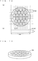
- a planar structure of the common cathode 24 provided on a cross section of the flow passage may be, as illustrated in FIGS. 4(a), 4(b) and 4(c) and the like, a parallel bar structure having band-like openings, in which a plurality of bar bodies are arrayed in one direction at an interval, a quadrangular grid structure having quadrangular openings, in which a plurality of bar bodies are arrayed in two directions at intervals, a concentric structure having annular or circular openings, in which a plurality of annular bodies are concentrically arranged, and the like, and in addition thereto, may be a honeycomb structure having regular hexagonal openings, a triangular grid structure having triangular openings, in which a plurality of bar bodies are arrayed in three directions at intervals, a perforated structure in which holes (through holes) having a circular, triangular, quadrangular, pentagonal, and hexagonal shape or the like are drilled into a plate, and the like, and a
- the common cathode 24 includes an opening-arrayed body having a planar structure in which openings through which the process gas passes are arrayed. It is desirable that the openings be arrayed over the whole of the cross-section of the flow passage of the process gas in order not to inhibit the flow of the process gas, and it is desirable that the openings be uniformly arrayed over the whole of the cross section of the flow passage of the process gas in order not to disturb uniformity of the flow of the process gas.
- the resin material such as the variety of organic synthetic resins or the inorganic material such as the ceramics and the glass is used.
- the organic resin material the phenol resin, the polyester resin, the epoxy resin, the polyimide resin, the fluorine resin or the like is used, and as the inorganic material, the ceramics or the glass is generally used.
- the material of the ceramics the alumina, the mullite, the beryllia, the aluminum nitride, the silicon carbide, the cordierite, the magnesia, the spinel, the silica, zirconia (ZrO 2 ) or the like is used.
- a size of a space where the electric discharge is generated is determined in response to the sample.
- a size of a distance between such electric discharge electrodes which generate the electric discharge is also determined in response to a type, pressure, flow rate and the like of the process gas, and to contents of the process, such as a peak voltage and maximum rise rate of the pulse voltage; however, is determined at approximately 3 mm to 40 mm.
- a pulse power supply 1 shown in FIG. 1 applies pulse voltages, in which polarities are equal to each other, and the maximum rise rate dV/dt is 100 to 600 kV/ ⁇ s or more (maximum: 1000 kV/ ⁇ s), individually to between the first anode 22 and the common cathode 24 and to between the second anode 23 and the common cathode 24 in the atmospheric pressure.
- the maximum rise rate dV/dt of the pulse voltages applied individually to between the first anode 22 and the common cathode 24 and to between the second anode 23 and the common cathode 24 is 100 kV/ ⁇ s or more, whereby, as shown in FIG.
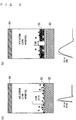
- the ion sheath layers 52a and 52b in which a thickness ⁇ d is thin are formed on upper surface side and lower surface side of the common cathode 24, and high-density ions and radicals, which are necessary for the reformation, are generated.
- the thickness ⁇ d of the ion sheath layers 52a and 52b formed on the upper surface side and lower surface side of the common cathode 24 shown in FIG. 2 is thickened, and densities of the ions and the radicals are lowered, and accordingly, efficiency of the reformation is low.
- the pulse width of the pulse voltage applied to between the anode 84 and the cathode 82 is a pulse width as short as approximately 50 to 300 ns in terms of a half-width, and the maximum rise rate dV/dt of the pulse voltage is roughly 100 to 600 kV/ ⁇ s or more, then the ion sheath layer 52 that is thin is formed on the upper surface side of the cathode 82, and high-density ions and radicals are generated. Meanwhile, as shown in FIG.
- the pulse width is a pulse width of approximately 1 to 10 ⁇ s in terms of the half-width, and the maximum rise rate dV/dt of the pulse voltage is roughly 100 kV/ ⁇ s or less, then the ion sheath layer 52 that is thick is formed on the upper surface side of the cathode 82, and accordingly, the densities of the generated ions and radicals become low.
- the repetition number of pulses is selected within a range where the arc discharge is not generated; however, is preferably approximately 1 kpps to several 10 kpps.
- the maximum rise rate dV/dt of the pulse voltage is roughly 100 to 600 kV/ ⁇ s or more, a glow discharge by ionization of the process gas is brought about, which is caused by an effect in which secondary electrons emitted when positive ions collide with the cathode 82 ionize molecules of the process gas and generate new positive ions, and by an impact ionization effect by the application of the pulse voltage with the high maximum rise rate dV/dt.
- the maximum rise rate dV/dt of the pulse voltage is roughly 100 to 600 kV/ ⁇ s or more (maximum: 1000 kV/ ⁇ s)
- the pulse width ⁇ t is roughly 50 ns
- growth of a plasma region made of streamers going from the anode 84 to the cathode 82 begins.
- the pulse width ⁇ t is roughly 50 to 100 ns
- the growth of the plasma region made of the streamers is ended at an initial stage where plasma regions made of short streamers are dispersed between the anode 84 and the cathode 82.
- the plasma region made of the streamers grows fully, and a state is brought where a plasma region made of branched long streamers is present between the anode 84 and the cathode 82.
- a streamer discharge in which the electric discharge is stopped at an initial stage of the growth of the plasma region made of the streamers is used in order that the anode 84 and the cathode 82 cannot be conducted to each other by the matter that the growth of the plasma region made of the streamer is advanced.
- the streamer discharge excellent in uniformity of the electric discharge is used, then the reformation can be carried out uniformly.
- the pulse width ⁇ t roughly reaches 400 ns to 1 ⁇ s or more, a local current concentration occurs owing to an excessively long application time of the pulse voltage, and the arc discharge is finally brought about.
- the pulse voltage with the high maximum rise rate dV/dt which does not reach the arc discharge, is applied to the process gas, whereby highly reactive active species which are activated more intensely and have high energy are generated, and highly reactive reform gas is generated.
- streamer discharge realization conditions where the pulse voltage with the pulse width, which does not cause the arc discharge, is obtained is selected in response to the shape of the reactor so that an appropriate amount of the active species can be generated as shown in FIG. 3(a) after the pulse voltage with the high maximum rise rate dV/dt is applied.
- FIGS. 4(a), 4(b) and 4(c) the planar structures of the common cathode 24 applied to the gas reforming device according to the first embodiment are illustrated.
- FIGS. 4(a), 4(b) and 4(c) states are shown, where the ion sheath layer 52a is expanded outward by a width ⁇ x from a central plasma region 51a made of the streamers.
- the common cathode 24 includes the grounding electrodes 45 on a peripheral portion of the flow passage of the process gas, and the grounding electrodes 45 are electrically connected to the ion sheath layer 52a, which is expanded outward by the width ⁇ x, on the peripheral portion of the flow passage of the process gas, whereby the ion sheath layer 52a is grounded.
- the common cathode 24 applied to the gas reforming device according to the first embodiment at least the surface thereof just needs to be made of the insulator (dielectric), and accordingly, the common cathode 24 may include a conductor such as metal in an inside thereof.
- FIG. 5 shows a schematic structure of principal portions of a gas reforming device (unipolar-type plasma reformer) serving as a base (basic structure) of first and second embodiments of the present disclosure.
- the unipolar-type plasma reformer includes: an anode 22u; and a cathode 24u that is arranged opposite to a tip end of the anode 22u, has a grid shape, has at least a surface thereof made of an insulator, and includes grounding electrodes 45u on peripheral portions thereof.
- the grounding electrodes 45u are brought into contact with end portions of an ion sheath layer 52u spread on the surface of the cathode 24u, whereby a ground potential is given to the ion sheath layer 52u, the process gas introduced in a direction parallel to the direction of such a shortest inter-electrode distance between the anode 22u and the cathode 24u is activated by plasma formed between the anode 22u and the cathode 24u, and the reform gas is generated.
- the pulse voltage is applied to between one anode 22u and one cathode 24u, and a plasma region 51u made of the streamers is formed by a unipolar-type discharge between the anode 22u and the cathode 24u.
- the ion sheath layer 52u is spread outward by the width ⁇ x from the central plasma region 51u made of the streamers, and accordingly, the ion sheath layer 52u is grounded in such a manner that the grounding electrodes 45u are electrically connected to the expanded ion sheath layer 52u.
- the grounding of the ion sheath layer 52u by the grounding electrodes 45u wasteful scattering of the electric discharge to other than the cathode 24 is prevented, and high energy is injected to between the anode 22u and the cathode 24u.
- the cathode 24u just needs to have the grid shape, and at least the surface thereof just needs to be made of the insulator, and accordingly, a conductor such as metal may be included in an inside thereof.
- FIG. 5 illustration of a gas reforming containers is omitted; however, in a similar way to the structure shown in FIG. 2 , the anode 22u and the cathode 24u are arranged in an inside of a cylindrical gas reforming container, the process gas is introduced from one end of a flow passage, and the reform gas activated by the plasma is jetted from other end of the flow passage.
- arrangement (positional relationship) of the anode 22u, the cathode 24u and the gas reforming container is determined so that the process gas can flow in the direction parallel to the direction (shortest inter-electrode distance direction) of the electric field.
- the discharge which gives the ground potential to the common cathode 24, applies the pulse voltages in which the polarities are equal to each other to the first anode 22 and the second anode 23, and generates the plasmas individually between the first anode 22 and the common cathode 24 and between the second anode 23 and the common cathodes 24, is referred to as a "bipolar-type discharge".
- a schematic voltage waveform of the pulse voltages is premised on the time of no load. This is because, even if the pulse power supply 1 is operated under the same conditions, if the specific configuration such as the intervals between the first anode 22 and the common cathode 24 and between the second anode 23 and the common cathode 24 and the structures of the first anode 22, the second anode 23 and the common cathode 24 is changed, then the schematic voltage waveform of the pulse voltages applied to between the first anode 22 and the common cathode 24 and to between the second anode 23 and the common cathode 24 come to differ.
- the pulse power supply 1 repeatedly applies the pulse voltages, which cause the streamer discharge without causing the arc discharge, between the first anode 22 and the common cathode 24, and between the second anode 23 and the common cathode 24. Specifically, the pulse power supply 1 repeatedly applies the pulse voltages with the pulse width of 50 to 300 ns in terms of the half-width between the first anode 22 and the common cathode 24 and between the second anode 23 and the common cathode 24.
- Example of a voltage waveform of the pulse voltages which the pulse power supply 1 applies between the first anode 22 and the common cathode 24 and between the second anode 23 and the common cathode 24 and example of a current waveform of a current flowing when the pulse voltages are applied are shown in FIG. 7 .
- changes of a voltage V2 of each pulse voltage and the current I2 flowing when the pulse voltage is applied are shown, and the pulse width has become approximately 100 ns in terms of the half-width.
- an inductive energy storage-type power supply circuit (hereinafter, referred to as an "IES circuit") shown in FIG. 1 in which a static induction-type thyristor (hereinafter, referred to as a "SI thyristor”) is used.
- the IES circuit performs turn off by using an opening switch function of the SI thyristor as well as a closing switch function thereof, and by the turn off concerned, generates a high voltage between a gate and anode of the SI thyristor. Note that details of the IES circuit are described in "Extremely Short Pulse Generation Circuit (IES Circuit) by SI Thyristor", by IIDA Katsuji and SAKUMA Takeshi, Lecture Collection of SI Device Symposium (2002).
- the pulse power supply 1 includes a low-voltage direct-current power supply 131.
- a voltage E of the low-voltage direct-current power supply 131 is permitted to be significantly lower than the peak voltage of the pulse voltage which the pulse power supply 1 generates. For example, even if a peak voltage generated on both ends of a primary winding 133 reaches several kilovolts, the voltage E of the low-voltage direct-current power supply 131 is permitted to be several ten volts.
- a lower limit of the voltage E is decided at a latching voltage of an SI thyristor 134 to be described later or more.
- the pulse power supply 1 is capable of using the low-voltage direct-current power supply 131 as an electric energy source, and accordingly, is constructible to be compact at low cost.
- the pulse power supply 1 includes a capacitor 132 connected in parallel to the low-voltage direct-current power supply 131.
- the capacitor 132 apparently lowers impedance of the low-voltage direct-current power supply 131, and thereby strengthens an electric discharge capability of the low-voltage direct-current power supply 131.
- the pulse power supply 1 includes the primary winding 133, the SI thyristor 134, a MOSFET 135, a gate drive circuit 136 and a diode 137.
- the primary winding 133 is inductively coupled to a secondary winding 138 connected between a high voltage output terminal O 2 and a ground terminal O 1 , and configures a step-up transformer.
- a turns ratio of the primary winding 133 and the secondary winding 138 is decided by a required electric discharge voltage.
- the secondary winding inductively coupled to the primary winding 133 may be increased to two, the anode 22 may be connected to one of the secondary windings, and the anode 23 may be connected to the other secondary winding.
- a positive electrode of the low-voltage direct-current power supply 131 and one end of the primary winding 133 are connected to each other, the other end of the primary winding 133 and an anode of the SI thyristor 134 are connected to each other, the anode of the SI thyristor 134 and a drain of the FET 135 are connected to each other, and a source of the FET 135 and a negative electrode of the low - voltage direct-current power supply 131 are connected to each other.
- the gate of the SI thyristor 134 and an anode of the diode 137 are connected to each other, and a cathode of the diode 137 and one end (positive electrode of the low-voltage direct-current power supply 131) of the primary winding 133 are connected to each other.
- the gate drive circuit 136 is connected to the gate and source of the FET 135.
- the SI thyristor 134 is capable of turning on and turning off in response to a gate signal.
- the FET 135 is a switching element in which a conduction state between a drain and a source is changed in response to a gate signal V C given from the gate drive circuit 136. It is desirable that an ON-voltage or ON-resistance of the FET 135 be low. Moreover, a withstand voltage of the FET 135 is required to be higher than the voltage E of the low-voltage direct-current power supply 131.
- the diode 137 is provided in order to inhibit a current flowing in the case of giving a positive bias to the gate of the SI thyristor 134, that is, in order that the SI thyristor 134 cannot be current driven in the case of giving the positive bias to the gate of the SI thyristor 134.
- FIG. 6 shows: (a) a change of the gate signal V C , which is given to the FET 135, with respect to the time (axis of abscissas); (b) a change of a conduction state of the SI thyristor 134 with respect to the time (axis of abscissas); (c) a change of the current I L flowing through the primary winding 133 with respect to the time (axis of abscissas); (d) a change of the voltage V L , which is generated on both ends of the primary winding 133, with respect to the time (axis of abscissas); and (e) a change of the voltage V AG (axis of ordinates) between the anode and gate of the SI thyristor 134 with respect to the time (axis of abscissas).
- a gas reforming device in a similar way to the structure shown in FIG. 2 , includes: a first anode 22 and a second anode 23, which are arranged opposite to each other; and a common cathode 24 including a grid-like insulator sandwiched between respective tip ends of the first anode 22 and the second anode 23 so as to be spaced apart therefrom, and including grounding electrodes 45 on peripheral portions thereof.
- a ground potential is given to the common cathode 24, pulse voltages in which polarities are equal to each other are applied to the first anode 22 and the second anode 23, and bipolar-type plasmas are generated individually between the first anode 22 and the common cathode 24 and the second anode 23 and the common cathode 24.
- the first anode 22 and the second anode 23 are inserted into a portion circular in cross section in a center portion of a gas reforming container 21, which have L-pipes connected to both sides thereof, from a direction parallel to the direction where the process gas flows.
- the common cathode 24 is inserted into the portion circular in cross section in the center portion of the gas reforming container 21.
- the first electrode structure 56 and the second electrode structure 57 are bent at boundaries between the first bar-like portions 54 and 57 and the second bar-like portions 55 and 58, and are inserted into the flow passage from the direction perpendicular to the direction where the process gas flows.
- the gas reforming device shown in FIG. 8 is different from the gas reforming device shown in FIG. 2 in that the process gas is introduced through the left-side L-pipe into a left side of the portion circular in cross section in the center portion, that the reform gas activated by the bipolar-type plasmas is jetted through the right-side L-pipe from a right side of the portion circular in cross section in the center portion, and that a surface of a sample (not shown) placed on the outside of the gas reforming container 21 is treated.
- Others are substantially similar to those of the gas reforming device shown in FIG. 2 , and accordingly, a duplicate description is omitted.
- a gas reforming device in a similar way to the gas reforming device shown in FIG. 2 , includes: a plurality of first anodes 22 ij and a plurality of second anodes 23 ij , which are arranged opposite to each other; and a common cathode 24h that is sandwiched between respective tip ends of the plurality of first anodes 22 ij and the plurality of second anodes 23 ij so as to be spaced apart therefrom, includes a grid-like insulator, and includes grounding electrodes (not shown) on peripheral portions thereof.
- the plurality of first anodes 22 ij and the plurality of second anodes 23 ij have a bar shape, and are arranged parallel to one another.
- the respective tip ends of the plurality of first anodes 22 ij and the plurality of second anodes 23 ij are spaced apart from surfaces of the common cathode 24 by the same distance.
- the plurality of first anodes 22 ij and the plurality of second anodes 23 ij are fixed to the inside of the gas reforming container 21 by holding members 63 made of an insulator.
- the plurality of first anodes 22 ij are electrically connected to the high voltage output terminal O 2 through a power feed member 65, and the plurality of second anodes 23ij are electrically connected to the high voltage output terminal O 2 through a power feed member 66.
- the ground potential is given to the common cathode 24h, and the pulse voltages in which the polarities are equal to each other are applied to the plurality of first anodes 22 ij and the plurality of second anodes 23 ij , and the bipolar-type plasmas are generated individually between the plurality of first anodes 22 ij and the common cathode 24h and between the plurality of second anodes 23 ij and the common cathode 24h.
- the plurality of first anodes 22 ij are arranged at center portions of respective holes of an insulating plate 61 shown in FIG. 11 and FIG. 12 , in which a plurality of circular holes (through holes) are opened, and are then separated from one another, and the plurality of second anodes 23 ij are arranged at center portions of respective holes of an insulating plate 62 shown in FIG. 11 and FIG. 12 , in which a plurality of circular holes are opened, and are then separated from one another.
- a planar structure of the common cathode 24h is an insulating plate in which a plurality of circular holes (through holes) are opened.
- a structure of the second modification example realizes a cathode hollow-type reformer that generates the electrode injection uniformly on the entire surface.
- the plurality of first anodes 22 ij and the plurality of second anodes 23 ij and the common cathode 24h are housed in the inside of the cylindrical gas reforming container 21.
- the process gas is introduced upward from one end of the flow passage, which is located at a bottom portion of the gas reforming container 21 in FIG. 9 and FIG. 10
- the reform gas activated by the bipolar-type plasmas is jetted from the other end of the flow passage, which is located at an upper portion of the gas reforming container 21, to a sample (not shown) placed above the gas reforming container 21, and a surface of the sample is treated.
- Others are substantially similar to those of the gas reforming container shown in FIG. 2 , and accordingly, a duplicate description is omitted.
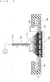
- a gas reforming device in accordance with a preferred embodiment of the present invention, includes: a first cathode 64 and a second cathode 65, which are arranged opposite to each other, individually include grid-like insulators, and individually include grounding electrodes (not shown) on peripheral portions thereof; and common anodes 92 and 93 which are sandwiched between surfaces (opposite surfaces) of the first cathode 64 and the second cathode 65 so as to be spaced apart therefrom.
- the grounding electrodes are individually brought into contact with end portions of ion sheath layers individually spread on the surfaces of the first cathode 64 and the second cathode 65, whereby the ground potential is given individually to the ion sheath layers, and the process gas introduced in a direction parallel to a direction of a shortest inter-electrode distances between the first cathode 64 and the common anodes 92 and between the second cathode 65 and the common anodes 93 is activated by plasmas individually formed between the first cathode 64 and the common anodes 92 and between the second cathode 65 and the common anodes 63, and the reform gas is generated.
- the first cathode 64 and the second cathode 65 are inserted from an outside of a cylindrical gas reforming container 81d into an inside thereof.
- the common anodes 92 and 93 are housed in the inside of the gas reforming container 81d.
- the gas reforming container 81d is connected to a left-side pipe 81e through an O-ring 73a and a center ring 72a.
- the O-ring 73a between the gas reforming container 81d and the left-side pipe 81e is compressed by a clamp 71a, and keeps a tight vacuum.
- the gas reforming container 81d is connected to a right-side pipe 81f through an O-ring 73b and a center ring 72b.
- the O-ring 73b between the gas reforming container 81d and the right-side pipe 81f is compressed by a clamp 71b, and keeps a tight vacuum.
- the process gas is introduced into an inside of a gas reforming container 81e from one end of a flow passage, which is located at a left-side end portion of FIG. 14 , reform gas activated by double unipolar-type plasmas is jetted to a sample (not shown), which is placed on an outside of the gas reforming container 81f, from the other end of the flow passage, which is located at a right-side end portion of a gas reforming container 81f, and a surface of the sample is treated.
- the process gas is selected in response to process contents of the gas reforming container 81d.
- the process gas may be nitrogen gas with high purity, gas of highly active elemental chlorine or chloride, or may be highly active gas such as halide (fluoride, bromide, iodide or the like) other than the chloride.
- the process gas may be other gas such as mixed gas of any of these highly active gases and the nitrogen gas, rare gas or the like.
- the process gas in response to the usage purpose of the reform gas, such as the surface treatment, the process gas may be gas of air, oxygen or an oxygen compound. Purity, dew point and the like of the process gas are selected in response to the usage purpose of the surface treatment.
- the left-side common anodes 92 are coated with tubular protection dielectrics 69
- the right-side common anodes 93 are coated with tubular protection dielectrics 69.
- a ceramic coating method, a gel casting method, a glass method and the like are used for the coating for the left-side common anodes 92 with the protection dielectrics 69 and the coating for the right-side common anodes 93 with the protection dielectrics 69.
- the left-side common anodes 92 and the right-side common anodes 93 are fixed to the inside of the gas reforming container 81d through holding members 67 made of an insulator and holding members 68 made of an insulator, respectively.
- first cathode 64 and the second cathode 65 at least the surfaces thereof just need to be made of an insulator (dielectric), and accordingly, the first cathode 64 and the second cathode 65 may include conductors such as metal in insides thereof.
- the left-side common anodes 92 and the right-side common anodes 93 are short-circuited to potentials equal to each other by plate-like introduction wires 91 shown in FIG. 15 , and are further connected to an external pulse power supply (not shown). Pulse voltages in which the maximum rise rate dV/dt is 100 to 600 kV/ ⁇ s or more (maximum: 1000 kV/ ⁇ s) are individually applied to between the first cathode 64 and the common anodes 92 and to between the second cathode 65 and the common anodes 93.
- a pulse width of the pulse voltages be approximately 50 to 300 ns in terms of the half-width, and it is preferable that the repetition number of pulses be approximately 1 kpps to several 10 kpps.
- Others are substantially similar to those of the gas reforming device according to the first embodiment, and accordingly, a duplicate description is omitted.
- the process gas introduced in the direction parallel to the direction of the shortest inter-electrode distances between the first cathode 64 and the common anodes 92 and between the second cathode 65 and the common anodes 93 is activated, the reform gas is thereby generated, the reform gas is jetted from one end of the flow passage, which is located on the right-side end portion of the gas reforming container 81f, to the sample (not shown) placed on the outside, and a surface of the sample is treated.
- FIG. 16 shows data in which an effect of a remote plasma method of treating a surface of a quartz plate by the reform gas activated by the plasma reformer is compared among Examples 1 to 3 and Comparative examples 1 and 2.
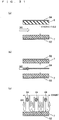
- a description regarding an effect of reforming a surface of a sample 5 is shown in FIG. 30 .
- the reform gas jetted as remote plasma reforms a surface layer of the sample 5, whereby a state of the surface of the sample 5 is changed from a state shown in FIG. 30(a) , where surface energy is low and activity of the surface is low, to a state view shown in FIG. 30(b) , where the surface energy is high and the activity of the surface is high, and hydrophilicity of the surface of the sample 5 is enhanced.
- FIG. 16 an effect in the case of introducing nitrogen gas into the plasma reformer at 5 L/second, jetting the reform gas activated by the plasma onto the quartz plate placed at a distance of 5 mm from a discharge port of the plasma reformer and treating the surface of the quartz plate is compared.
- Examples 1 to 3 and Comparative examples 1 and 2 are plotted while taking, on an axis of ordinates, a time (process time) required until the contact angle of the water with the quartz plate becomes 5 degrees or less after the process from 50 degrees before the process, and taking, on an axis of abscissas, input power necessary to generate the plasma.
- a time processing time
- abscissas input power necessary to generate the plasma.
- a cylindrical gas reforming container was used, and an area of an outlet side of a flow passage of the gas reforming container that jets the reform gas was set at 2 cm 2 in each thereof.
- a pulse voltage was applied, in which a peak voltage is 20 kV, a pulse width is 100 ns, and the repetition number of pulses is 2 kpps.
- the plasma reformer used in Comparative example 1 shown on the upper left of FIG. 16 is a coaxial cylinder-type plasma reformer shown in FIG. 17 , in which a cylindrical cathode 82 is provided on an outer circumferential surface of a cylindrical gas reforming container 81 made of a dielectric (ceramics), and an anode 84 coated with a dielectric (ceramics) 83 is provided on a cylindrical axis on a center of the gas reforming container 81. As shown by arrows, the process gas was introduced into a flow passage in an inside of the gas reforming container 81 from a left side of FIG.
- the plasma reformer used in Comparative example 2 shown from the center of FIG. 16 to the lower right thereof is a parallel flat plate-type plasma reformer shown in FIG. 18 , in which a plate-like anode 84 is provided on an upper inner surface of a gas reforming container 85 made of a tubular dielectric (ceramics) rectangular in cross section, and a plate-like cathode 82 is provided on a lower inner surface of the gas reforming container 85. As shown by arrows, the process gas was introduced into a flow passage in an inside of the gas reforming container 85 from a left side of FIG.
- Example 1 located below Comparative example 1 corresponds to the base (basic structure) of the first and second embodiments, and shows an effect in the case of the unipolar-type plasma reformer shown in FIG. 19 , which includes, in the inside of the gas reforming container 81 made of the cylindrical dielectric (ceramics), the cathode 24 including the grid-like insulator and including the grounding electrodes (not shown) on the peripheral portions thereof, and the anode 22u that allows the tip end portion thereof to be opposed to the cathode 24. As shown by arrows, the process gas was introduced into the flow passage in the inside of the gas reforming container 81 from a left side of FIG.
- the reform gas activated by the unipolar-type plasma was jetted from one end of the flow passage, which was located on the right-side end portion of the gas reforming container 81, onto the quartz plate placed on the outside of the gas reforming container 81, and the surface of the quartz plate was treated.
- the ground potential was given to the cathode 24, and the plasma region 51u containing the plasma is formed between the cathode 24 and the anode 22u.
- a process time by the remote plasma is approximately 8 to 16 minutes, and the process efficiency is improved in comparison with Comparative example 1.
- Example 2 located below Comparative example 2 corresponds to the second embodiment, and shows an effect in the case of the double unipolar-type plasma reformer shown in FIG. 20 , which includes, in the inside of the gas reforming container 81 made of the cylindrical dielectric (ceramics), the first and second cathodes 64 and 65 arranged opposite to each other, individually including the grid-like insulators, and individually including the grounding electrodes (not shown) on the peripheral portions thereof, and the common anodes (92, 93) sandwiched between the respective tip ends of the first cathode 64 and the second cathode 65 so as to be spaced apart therefrom.
- the common anode 92 and the common anode 93 are individually coated with the protection dielectrics 69.
- the introduction wires 91 to the common anode 92 and the common anode 93 are also coated with the protection dielectrics 69.
- the process gas was introduced into the flow passage in the inside of the gas reforming container 81 from a left side of FIG. 20 to a right side thereof, the reform gas activated by the double unipolar-type plasma was jetted from one end of the flow passage, which was located on the right-side end portion of the gas reforming container 81, onto the quartz plate placed on the outside of the gas reforming container 81, and the surface of the quartz plate was treated.
- the ground potential is given to the first cathode 64 and the second cathode 65, and plasma regions 51p and 51q of non-thermal equilibrium plasma are individually formed between the first cathode 64 and the common anode 92 and between the second cathode 65 and the common anode 93.
- the process time by the remote plasma is approximately 3 to 7 minutes, and it is understood that the process efficiency is considerably improved in comparison with Comparative examples 1 and 2.
- Example 3 located on the lower left of FIG. 16 corresponds to the first embodiment, and shows an effect in the case of the bipolar-type plasma reformer shown in FIG. 21 , which includes, in the insides of the gas reforming containers 21a and 21b made of the cylindrical dielectrics (ceramics), the first and second anodes 22 and 23 arranged opposite to each other, and the common cathode 24 that is sandwiched between the respective tip ends of the first anode 22 and the second anode 23 so as to be spaced apart therefrom, includes the grid-like insulator, and includes grounding electrodes 45 on the peripheral portions thereof.
- the process gas was introduced into the flow passage in the inside of the gas reforming container 81 from a left side of the gas reforming container 21a in FIG. 21 to a right side thereof, the reform gas activated by the bipolar-type plasma was jetted from one end of the flow passage, which was located on the right-side end portion of the gas reforming container 21b, onto the quartz plate placed on the outside of the gas reforming container 21b, and the surface of the quartz plate was treated.
- the first anode 22 is coated with the protection dielectric 41
- the second anode 23 is coated with the protection dielectric 42.
- the ground potential is given to the common cathode 24, and the pulses in which the polarities are equal to each other are applied to the first anode 22 and the second anode 23, and plasma regions 51a and 51b including the plasmas are formed between the first anode 22 and the common cathode 24 and between the second anode 23 and the common cathode 24, respectively.
- the process time by the remote plasma is approximately 11 to 2 minutes, and the process efficiency is improved in comparison with Examples 1 and 2.
- FIG. 22 shows a structure of an anode 22 suitable for use in the bipolar-type plasma reformer or the unipolar-type plasma reformer, and shows a state where the plasma region 51a including the plasma is formed from the tip end of the anode 22 in a state where the metal-made anode 22 is coated with the protection dielectrics 41a, 41b and 41c by using the ceramic coating method, the gel casting method, the glass method or the like.
- FIG. 23 shows a structure of common anodes 92 and 93 suitable for use in the double unipolar-type plasma reformer, and shows a state where, in a state where the metal-made anodes 92 and 93 are coated with the protection dielectrics 69a, 69b and 69c by using the ceramic coating method, the gel casting method, the glass method or the like, the plasma region 51p including the plasma is formed from the tip end on the left side of the anode 92, and the plasma region 51q including the plasma is formed from the tip end on the right side of the anode 93.
- the introduction wires 91 to the metal-made anodes 92 and 93 are also coated with the protection dielectrics 69d by using the ceramic coating method, the gel casting method, the glass method or the like.
- FIG. 24(a) shows a structure of an anode 22p suitable for use in the bipolar-type plasma reformer or the unipolar-type plasma reformer, and shows a state where the plasma region 51u including the plasma is formed from the tip end of the metal-made anode 22p in a state where the anode 22p is coated with a protection dielectric 41p by using the ceramic coating method, the gel casting method, the glass method or the like.
- FIG. 24(b) shows a case where the anode 22p with the structure shown in FIG.
- FIG. 24(a) is used for the double unipolar-type plasma reformer, and shows a state where the plasma region 51p including the plasma is generated from the left side of the tip end of the anode 22p and the plasma region 51q including the plasma is formed from the right side of the tip end thereof.
- the bar-like portions including the tip ends are extended in the direction perpendicular to the direction where the process gas flows. Moreover, balls larger in diameter than the bar-like portions are formed on the tip ends. In such a way, spots other than the tip ends are suppressed from becoming starting points of the electric discharge.
- FIG. 25(a) shows a structure of an anode 61p suitable for use in the bipolar-type plasma reformer or the unipolar-type plasma reformer, and shows a state where the plasma region 51u including the plasma is formed from the tip end of the metal-made anode 61p in a state where the anode 61p is coated with the protection dielectric 69p by using the ceramic coating method, the gel casting method, the glass method or the like.
- FIG. 25(b) shows a case where the anode 61p having the structure shown in FIG.
- 25(a) is used for the double unipolar-type plasma reformer, and shows a state where the plasma region 51p including the plasma is formed from the left side of the tip end 61p and the plasma region 51q of the non-thermal equilibrium plasma is formed from the right side thereof.
- FIG. 26 to FIG. 29 show structures of anodes formed of conductive ceramics such as silicon carbide (SiC) with electrical resistivity of approximately 10 ⁇ • cm.
- FIG. 26 shows a structure of an anode 22r suitable for use in the bipolar type-plasma reformer or the unipolar-type plasma reformer, and shows a state where the plasma region 51u including the plasma is formed from a tip end of the anode 22r.
- FIG. 27 shows a structure of an anode 61r suitable for use in the double unipolar-type plasma reformer, and shows a state where the plasma region 51p including the plasma is formed from a left-side tip end of the anode 61r and the plasma region 51q including the plasma is formed from a right-side tip end thereof.
- FIG. 28(a) shows a structure of an anode 22s in a case of being used for the bipolar-type plasma reformer or the unipolar-type plasma reformer, and shows a state where the plasma region 51u including the plasma is formed from a tip end of the anode 22s.
- FIG. 28(b) shows a case of using the anode 22s having the structure of FIG. 28(a) for the double unipolar-type plasma reformer, and shows a state where the plasma region 51p including the plasma is formed from a left side of a tip end of the anode 22s and the plasma region 51q including the plasma is formed from a right side of the tip end.
- FIG. 29(a) shows a structure of an anode 61p in a case of being used for the bipolar-type plasma reformer or the unipolar-type plasma reformer, and shows a state where the plasma region 51u including the plasma is formed from a tip end of the anode 61s.
- FIG. 29(b) shows a case of using the anode 61s having the structure of FIG. 29(a) for the double unipolar-type plasma reformer, and shows a state where the plasma region 51p including the plasma is formed from a left side of a tip end of the anode 61s and a plasma region 51q of the non-thermal equilibrium plasma is formed from a right side of the tip end.
Landscapes
- Chemical & Material Sciences (AREA)
- Engineering & Computer Science (AREA)
- Physics & Mathematics (AREA)
- General Health & Medical Sciences (AREA)
- Health & Medical Sciences (AREA)
- Organic Chemistry (AREA)
- Chemical Kinetics & Catalysis (AREA)
- Electromagnetism (AREA)
- Toxicology (AREA)
- Plasma & Fusion (AREA)
- Mechanical Engineering (AREA)
- Combustion & Propulsion (AREA)
- Inorganic Chemistry (AREA)
- Spectroscopy & Molecular Physics (AREA)
- Plasma Technology (AREA)
- Physical Or Chemical Processes And Apparatus (AREA)
Claims (10)
- Gasreformierungsvorrichtung, umfassend:einen Gasströmungskanalformkörper (81d);eine erste und eine zweite Kathode (64, 65), die in dem Gasströmungskanal einander gegenüberliegend angeordnet sind, wobei sie jeweils eine Gitterform aufweisen und zumindest die Oberflächen derselben aus einem Isolator hergestellt sind;eine gemeinsame Anode (93), die zwischen den jeweiligen Oberflächen der ersten und der zweiten Kathode (64, 65) sandwichartig dazwischenliegend angeordnet ist, um so von diesen in die zur Gasströmungsrichtung im Gasströmungskanal parallele Richtung beabstandet angeordnet zu sein, undeine Pulsleistungsversorgung (1) zum Anlegen einer Pulsspannung zwischen der ersten Kathode (64) und der gemeinsamen Anode, (93) und zwischen der zweiten Kathode (65) und der gemeinsamen Anode, um so Ionenhüllenschichten zu erzeugen, die über die jeweiligen Oberflächen der ersten und der zweiten Kathode (64, 65) verteilt sind,wobei die erste und die zweite Kathode (64, 65) jeweils mit Masseelektroden (45) versehen sind, die auf Umfangsabschnitten von diesen angeordnet sind, um so während des Betriebs Kontakt mit Endabschnitten der Ionenhüllenschichten herzustellen, wodurch die Ionenhüllenschichten mit Masse verbunden werden,wobei während des Betriebs die Pulsleistungsversorgung (1) konfiguriert ist, aus einem Prozessgas, das in eine zu einer Richtung von kürzesten Elektroden-Zwischen-Abständen zwischen der ersten Kathode (64) und der gemeinsamen Anode (93), und zwischen der zweiten Kathode (65) und der gemeinsamen Anode (93) parallele Richtung eingeleitet wird, jeweils nicht-thermische Gleichgewichts-Tieftemperaturplasmen zwischen der ersten Kathode (64) und der gemeinsamen Anode (93), und zwischen der zweiten Kathode (65) und der gemeinsamen Anode (93) auszubilden, und wobei die nicht-thermischen Gleichgewichts-Tieftemperaturplasmen konfiguriert sind, das Prozessgas zu aktivieren, um so ein Reformgas zu erzeugen.
- Gasreformierungsvorrichtung gemäß Anspruch 1, wobei die Pulsleistungsversorgung (1) ausgelegt ist, Pulsspannungen anzulegen, in denen eine Maximalanstiegsrate dV/dt 100 bis 1000 kV/µs jeweils zwischen der ersten Kathode (64) und der gemeinsamen Anode (93), und zwischen der zweiten Kathode (65) und der gemeinsamen Anode (93) ist.
- Gasreformierungsvorrichtung gemäß Anspruch 1 oder 2, wobei die Pulsleistungsversorgung (1) ferner ausgelegt ist, Pulsspannungen mit einer Halbwertsbreite von 50 bis 300 ns anzulegen.
- Gasreformierungsvorrichtung gemäß einem der Ansprüche 1 bis 3, wobei die Pulsleistungsversorgung (1) einen SI-Thyristor (134) zum Erzeugen der Pulsspannung umfasst.
- Verfahren zum Betreiben einer Gasreformierungsvorrichtung gemäß Anspruch 1, wobei das Verfahren Folgendes umfasst:Einleiten von Prozessgas in eine zu einer Richtung von kürzesten Elektroden-Zwischen-Abständen zwischen der ersten Kathode (64) und der gemeinsamen Anode (93), und zwischen der zweiten Kathode (65) und der gemeinsamen Anode (93) parallele Richtung;Anlegen einer Pulsspannung zwischen der ersten Kathode (64) und der gemeinsamen Anode (93), und zwischen der zweiten Kathode (65) und der gemeinsamen Anode (93);Erzeugen von über die jeweiligen Oberflächen der ersten und der zweiten Kathode verteilten Ionenhüllenschichten;Verbinden der Ionenhüllenschichten mit Masse durch In-Kontakt-Bringen von Endabschnitten der Ionenhüllenschichten mit den Masseelektroden (45);Ausbilden von nicht-thermischen Gleichgewichts-Tieftemperaturplasmen jeweils zwischen der ersten Kathode (64) und der gemeinsamen Anode (93), und zwischen der zweiten Kathode (65) und der gemeinsamen Anode (93) durch Anlegen der Pulsspannung;Aktivieren des Prozessgases durch die nicht-thermischen Gleichgewichts-Tieftemperaturplasmen;Erzeugen des reformierten Gases durch die Aktivierung.
- Verfahren gemäß Anspruch 5, wobei die Pulsspannung als Pulsspannungen angelegt wird, in denen eine Maximalanstiegsrate dV/dt 100 bis 1000 kV/µs jeweils zwischen der ersten Kathode (64) und der gemeinsamen Anode (93), und zwischen der zweiten Kathode (65) und der gemeinsamen Anode (93) ist.
- Verfahren gemäß Anspruch 5 oder 6, wobei Drücke zwischen der ersten Kathode (64) und der gemeinsamen Anode (93), und zwischen der zweiten Kathode (65) und der gemeinsamen Anode (93) ein Atmosphärendruck sind.
- Verfahren gemäß Anspruch 5 oder 6, wobei Drücke zwischen der ersten Kathode (64) und der gemeinsamen Anode (93), und zwischen der zweiten Kathode (65) und der gemeinsamen Anode (93) in einem druckverminderten Zustand mit einem Druck von 10 kPa oder mehr sind.
- Verfahren gemäß einem der Ansprüche 5 bis 8, wobei die Pulsbreite der Pulsspannungen 50 bis 300 ns in Bezug auf eine Halbwertsbreite ist.
- Verfahren gemäß einem der Ansprüche 5 bis 9, wobei die Pulsspannungen unter Anwendung eines SI-Thyristors (134) erzeugt werden.
Applications Claiming Priority (2)
| Application Number | Priority Date | Filing Date | Title |
|---|---|---|---|
| JP2008207397 | 2008-08-11 | ||
| PCT/JP2009/063984 WO2010018783A1 (ja) | 2008-08-11 | 2009-08-07 | ガス改質装置 |
Publications (3)
| Publication Number | Publication Date |
|---|---|
| EP2317829A1 EP2317829A1 (de) | 2011-05-04 |
| EP2317829A4 EP2317829A4 (de) | 2014-09-24 |
| EP2317829B1 true EP2317829B1 (de) | 2018-12-05 |
Family
ID=41668928
Family Applications (1)
| Application Number | Title | Priority Date | Filing Date |
|---|---|---|---|
| EP09806675.6A Not-in-force EP2317829B1 (de) | 2008-08-11 | 2009-08-07 | Gasreformierungsvorrichtung und betriebsverfahren dafür |
Country Status (4)
| Country | Link |
|---|---|
| US (1) | US8454899B2 (de) |
| EP (1) | EP2317829B1 (de) |
| JP (1) | JP5597133B2 (de) |
| WO (1) | WO2010018783A1 (de) |
Families Citing this family (6)
| Publication number | Priority date | Publication date | Assignee | Title |
|---|---|---|---|---|
| EP2665347A4 (de) * | 2011-03-09 | 2014-11-05 | Ngk Insulators Ltd | Reaktorstruktur und plasmaverarbeitungsvorrichtung |
| IN2012CH05191A (de) * | 2012-12-13 | 2015-07-10 | Krupakar Murali Subramanian | |
| JP6208968B2 (ja) * | 2013-04-08 | 2017-10-04 | Global Energy Trade株式会社 | 水処理方法及び水処理装置 |
| CN107079574B (zh) * | 2014-10-21 | 2020-10-30 | 爱德华多·L·科班基亚特 | 用于提高燃烧效率并使燃烧污染物最小化的氧激发系统 |
| CN107409464A (zh) * | 2015-03-20 | 2017-11-28 | 日本碍子株式会社 | 等离子发生方法及杀菌水生成方法 |
| JP6641072B1 (ja) * | 2019-04-23 | 2020-02-05 | 三菱電機株式会社 | ガス製造システム及びガス製造方法 |
Citations (1)
| Publication number | Priority date | Publication date | Assignee | Title |
|---|---|---|---|---|
| JP2003001104A (ja) * | 2001-06-19 | 2003-01-07 | Daikin Ind Ltd | プラズマ反応器 |
Family Cites Families (13)
| Publication number | Priority date | Publication date | Assignee | Title |
|---|---|---|---|---|
| JP3147193B2 (ja) * | 1992-06-24 | 2001-03-19 | いすゞ自動車株式会社 | ディーゼル機関の排気ガス浄化システム |
| JP2001118699A (ja) * | 1999-10-15 | 2001-04-27 | Tdk Corp | プラズマ処理装置およびプラズマ処理方法 |
| JP4378592B2 (ja) * | 2000-11-13 | 2009-12-09 | 株式会社安川電機 | 放電発生装置の制御方法 |
| JP4543603B2 (ja) * | 2001-05-28 | 2010-09-15 | ダイキン工業株式会社 | プラズマ式ガス浄化装置及びストリーマ放電回路 |
| US6744212B2 (en) * | 2002-02-14 | 2004-06-01 | Lam Research Corporation | Plasma processing apparatus and method for confining an RF plasma under very high gas flow and RF power density conditions |
| US7511246B2 (en) * | 2002-12-12 | 2009-03-31 | Perkinelmer Las Inc. | Induction device for generating a plasma |
| WO2004054703A1 (en) * | 2002-12-13 | 2004-07-01 | Blue Planet Co., Ltd. | Plasma reactor and electrode plate used in the same |
| US7042159B2 (en) * | 2004-02-10 | 2006-05-09 | Daikin Industries, Ltd. | Plasma reactor and purification equipment |
| JP4321308B2 (ja) | 2004-03-02 | 2009-08-26 | パナソニック株式会社 | プラズマ発生方法及び装置 |
| JP4334004B2 (ja) | 2004-09-30 | 2009-09-16 | キヤノン株式会社 | プラズマ放電リアクターおよびガス処理装置 |
| US7914692B2 (en) | 2006-08-29 | 2011-03-29 | Ngk Insulators, Ltd. | Methods of generating plasma, of etching an organic material film, of generating minus ions, of oxidation and nitriding |
| JP4963923B2 (ja) * | 2006-10-06 | 2012-06-27 | 日本碍子株式会社 | 表面改質装置 |
| US8262847B2 (en) * | 2006-12-29 | 2012-09-11 | Lam Research Corporation | Plasma-enhanced substrate processing method and apparatus |
-
2009
- 2009-08-07 EP EP09806675.6A patent/EP2317829B1/de not_active Not-in-force
- 2009-08-07 JP JP2010524717A patent/JP5597133B2/ja not_active Expired - Fee Related
- 2009-08-07 WO PCT/JP2009/063984 patent/WO2010018783A1/ja not_active Ceased
-
2011
- 2011-02-07 US US13/021,968 patent/US8454899B2/en not_active Expired - Fee Related
Patent Citations (1)
| Publication number | Priority date | Publication date | Assignee | Title |
|---|---|---|---|---|
| JP2003001104A (ja) * | 2001-06-19 | 2003-01-07 | Daikin Ind Ltd | プラズマ反応器 |
Also Published As
| Publication number | Publication date |
|---|---|
| JP5597133B2 (ja) | 2014-10-01 |
| JPWO2010018783A1 (ja) | 2012-01-26 |
| US8454899B2 (en) | 2013-06-04 |
| WO2010018783A1 (ja) | 2010-02-18 |
| EP2317829A1 (de) | 2011-05-04 |
| EP2317829A4 (de) | 2014-09-24 |
| US20110135542A1 (en) | 2011-06-09 |
Similar Documents
| Publication | Publication Date | Title |
|---|---|---|
| Schutze et al. | The atmospheric-pressure plasma jet: a review and comparison to other plasma sources | |
| ES2882544T3 (es) | Aparato y método para la ignición por plasma con un dispositivo autorresonante | |
| US6441554B1 (en) | Apparatus for generating low temperature plasma at atmospheric pressure | |
| US8454899B2 (en) | Gas reforming device | |
| JP3990285B2 (ja) | 大気圧で低温プラズマを発生させる装置 | |
| Laimer et al. | Recent advances in the research on non‐equilibrium atmospheric pressure plasma jets | |
| US7572998B2 (en) | Method and device for creating a micro plasma jet | |
| AU6468898A (en) | Glow plasma discharge device | |
| US20140178604A1 (en) | Dual-Zone, Atmospheric-Pressure Plasma Reactor for Materials Processing | |
| JP2009128276A (ja) | 電離真空装置 | |
| Becker et al. | Microplasmas: scientific challenges & technological opportunities | |
| WO2006078888A2 (en) | Method and apparatus for cleaning and surface conditioning objects using plasma | |
| WO2002019379A1 (en) | Device and process for producing dc glow discharge | |
| KR101337047B1 (ko) | 상압 플라즈마 장치 | |
| EP4039640B1 (de) | Vorrichtung zur hocheffizienten kaltplasma-ozonerzeugung | |
| KR101692218B1 (ko) | 휘발성 유기 화합물 제거용 유전체 장벽 플라즈마 반응 장치 및 이를 이용한 휘발성 유기 화합물의 제거방법 | |
| US8092644B2 (en) | Method and apparatus for cleaning and surface conditioning objects using plasma | |
| JP5193641B2 (ja) | プラズマ処理装置 | |
| JP4925600B2 (ja) | プラズマ発生装置およびこれを用いた成膜方法 | |
| US20160233055A1 (en) | Apparatus and Method for Metastable Enhanced Plasma Ignition | |
| TW202549427A (zh) | 環面電漿源及使用其之方法 | |
| Jiang et al. | Study on a novel high-pressure micro-discharge configuration for micro-laser | |
| Chao et al. | Study on a novel high-pressure micro-discharge configuration for micro-laser |
Legal Events
| Date | Code | Title | Description |
|---|---|---|---|
| PUAI | Public reference made under article 153(3) epc to a published international application that has entered the european phase |
Free format text: ORIGINAL CODE: 0009012 |
|
| 17P | Request for examination filed |
Effective date: 20110224 |
|
| AK | Designated contracting states |
Kind code of ref document: A1 Designated state(s): AT BE BG CH CY CZ DE DK EE ES FI FR GB GR HR HU IE IS IT LI LT LU LV MC MK MT NL NO PL PT RO SE SI SK SM TR |
|
| AX | Request for extension of the european patent |
Extension state: AL BA RS |
|
| DAX | Request for extension of the european patent (deleted) | ||
| A4 | Supplementary search report drawn up and despatched |
Effective date: 20140825 |
|
| RIC1 | Information provided on ipc code assigned before grant |
Ipc: H05H 1/24 20060101AFI20140819BHEP Ipc: H05H 1/46 20060101ALI20140819BHEP Ipc: B01J 19/08 20060101ALI20140819BHEP |
|
| 17Q | First examination report despatched |
Effective date: 20160506 |
|
| STAA | Information on the status of an ep patent application or granted ep patent |
Free format text: STATUS: EXAMINATION IS IN PROGRESS |
|
| GRAP | Despatch of communication of intention to grant a patent |
Free format text: ORIGINAL CODE: EPIDOSNIGR1 |
|
| STAA | Information on the status of an ep patent application or granted ep patent |
Free format text: STATUS: GRANT OF PATENT IS INTENDED |
|
| INTG | Intention to grant announced |
Effective date: 20180615 |
|
| GRAS | Grant fee paid |
Free format text: ORIGINAL CODE: EPIDOSNIGR3 |
|
| GRAA | (expected) grant |
Free format text: ORIGINAL CODE: 0009210 |
|
| GRAA | (expected) grant |
Free format text: ORIGINAL CODE: 0009210 |
|
| STAA | Information on the status of an ep patent application or granted ep patent |
Free format text: STATUS: THE PATENT HAS BEEN GRANTED |
|
| AK | Designated contracting states |
Kind code of ref document: B1 Designated state(s): AT BE BG CH CY CZ DE DK EE ES FI FR GB GR HR HU IE IS IT LI LT LU LV MC MK MT NL NO PL PT RO SE SI SK SM TR |
|
| REG | Reference to a national code |
Ref country code: GB Ref legal event code: FG4D |
|
| REG | Reference to a national code |
Ref country code: CH Ref legal event code: EP |
|
| REG | Reference to a national code |
Ref country code: AT Ref legal event code: REF Ref document number: 1074741 Country of ref document: AT Kind code of ref document: T Effective date: 20181215 |
|
| REG | Reference to a national code |
Ref country code: IE Ref legal event code: FG4D |
|
| REG | Reference to a national code |
Ref country code: DE Ref legal event code: R096 Ref document number: 602009056079 Country of ref document: DE |
|
| REG | Reference to a national code |
Ref country code: NL Ref legal event code: MP Effective date: 20181205 |
|
| REG | Reference to a national code |
Ref country code: AT Ref legal event code: MK05 Ref document number: 1074741 Country of ref document: AT Kind code of ref document: T Effective date: 20181205 |
|
| REG | Reference to a national code |
Ref country code: LT Ref legal event code: MG4D |
|
| PG25 | Lapsed in a contracting state [announced via postgrant information from national office to epo] |
Ref country code: ES Free format text: LAPSE BECAUSE OF FAILURE TO SUBMIT A TRANSLATION OF THE DESCRIPTION OR TO PAY THE FEE WITHIN THE PRESCRIBED TIME-LIMIT Effective date: 20181205 Ref country code: NO Free format text: LAPSE BECAUSE OF FAILURE TO SUBMIT A TRANSLATION OF THE DESCRIPTION OR TO PAY THE FEE WITHIN THE PRESCRIBED TIME-LIMIT Effective date: 20190305 Ref country code: AT Free format text: LAPSE BECAUSE OF FAILURE TO SUBMIT A TRANSLATION OF THE DESCRIPTION OR TO PAY THE FEE WITHIN THE PRESCRIBED TIME-LIMIT Effective date: 20181205 Ref country code: BG Free format text: LAPSE BECAUSE OF FAILURE TO SUBMIT A TRANSLATION OF THE DESCRIPTION OR TO PAY THE FEE WITHIN THE PRESCRIBED TIME-LIMIT Effective date: 20190305 Ref country code: LT Free format text: LAPSE BECAUSE OF FAILURE TO SUBMIT A TRANSLATION OF THE DESCRIPTION OR TO PAY THE FEE WITHIN THE PRESCRIBED TIME-LIMIT Effective date: 20181205 Ref country code: FI Free format text: LAPSE BECAUSE OF FAILURE TO SUBMIT A TRANSLATION OF THE DESCRIPTION OR TO PAY THE FEE WITHIN THE PRESCRIBED TIME-LIMIT Effective date: 20181205 Ref country code: HR Free format text: LAPSE BECAUSE OF FAILURE TO SUBMIT A TRANSLATION OF THE DESCRIPTION OR TO PAY THE FEE WITHIN THE PRESCRIBED TIME-LIMIT Effective date: 20181205 Ref country code: LV Free format text: LAPSE BECAUSE OF FAILURE TO SUBMIT A TRANSLATION OF THE DESCRIPTION OR TO PAY THE FEE WITHIN THE PRESCRIBED TIME-LIMIT Effective date: 20181205 |
|
| PG25 | Lapsed in a contracting state [announced via postgrant information from national office to epo] |
Ref country code: SE Free format text: LAPSE BECAUSE OF FAILURE TO SUBMIT A TRANSLATION OF THE DESCRIPTION OR TO PAY THE FEE WITHIN THE PRESCRIBED TIME-LIMIT Effective date: 20181205 Ref country code: GR Free format text: LAPSE BECAUSE OF FAILURE TO SUBMIT A TRANSLATION OF THE DESCRIPTION OR TO PAY THE FEE WITHIN THE PRESCRIBED TIME-LIMIT Effective date: 20190306 |
|
| PG25 | Lapsed in a contracting state [announced via postgrant information from national office to epo] |
Ref country code: NL Free format text: LAPSE BECAUSE OF FAILURE TO SUBMIT A TRANSLATION OF THE DESCRIPTION OR TO PAY THE FEE WITHIN THE PRESCRIBED TIME-LIMIT Effective date: 20181205 |
|
| PG25 | Lapsed in a contracting state [announced via postgrant information from national office to epo] |
Ref country code: PL Free format text: LAPSE BECAUSE OF FAILURE TO SUBMIT A TRANSLATION OF THE DESCRIPTION OR TO PAY THE FEE WITHIN THE PRESCRIBED TIME-LIMIT Effective date: 20181205 Ref country code: CZ Free format text: LAPSE BECAUSE OF FAILURE TO SUBMIT A TRANSLATION OF THE DESCRIPTION OR TO PAY THE FEE WITHIN THE PRESCRIBED TIME-LIMIT Effective date: 20181205 Ref country code: PT Free format text: LAPSE BECAUSE OF FAILURE TO SUBMIT A TRANSLATION OF THE DESCRIPTION OR TO PAY THE FEE WITHIN THE PRESCRIBED TIME-LIMIT Effective date: 20190405 Ref country code: IT Free format text: LAPSE BECAUSE OF FAILURE TO SUBMIT A TRANSLATION OF THE DESCRIPTION OR TO PAY THE FEE WITHIN THE PRESCRIBED TIME-LIMIT Effective date: 20181205 |
|
| PG25 | Lapsed in a contracting state [announced via postgrant information from national office to epo] |
Ref country code: SK Free format text: LAPSE BECAUSE OF FAILURE TO SUBMIT A TRANSLATION OF THE DESCRIPTION OR TO PAY THE FEE WITHIN THE PRESCRIBED TIME-LIMIT Effective date: 20181205 Ref country code: IS Free format text: LAPSE BECAUSE OF FAILURE TO SUBMIT A TRANSLATION OF THE DESCRIPTION OR TO PAY THE FEE WITHIN THE PRESCRIBED TIME-LIMIT Effective date: 20190405 Ref country code: RO Free format text: LAPSE BECAUSE OF FAILURE TO SUBMIT A TRANSLATION OF THE DESCRIPTION OR TO PAY THE FEE WITHIN THE PRESCRIBED TIME-LIMIT Effective date: 20181205 Ref country code: SM Free format text: LAPSE BECAUSE OF FAILURE TO SUBMIT A TRANSLATION OF THE DESCRIPTION OR TO PAY THE FEE WITHIN THE PRESCRIBED TIME-LIMIT Effective date: 20181205 Ref country code: EE Free format text: LAPSE BECAUSE OF FAILURE TO SUBMIT A TRANSLATION OF THE DESCRIPTION OR TO PAY THE FEE WITHIN THE PRESCRIBED TIME-LIMIT Effective date: 20181205 |
|
| REG | Reference to a national code |
Ref country code: DE Ref legal event code: R097 Ref document number: 602009056079 Country of ref document: DE |
|
| PLBE | No opposition filed within time limit |
Free format text: ORIGINAL CODE: 0009261 |
|
| STAA | Information on the status of an ep patent application or granted ep patent |
Free format text: STATUS: NO OPPOSITION FILED WITHIN TIME LIMIT |
|
| PG25 | Lapsed in a contracting state [announced via postgrant information from national office to epo] |
Ref country code: DK Free format text: LAPSE BECAUSE OF FAILURE TO SUBMIT A TRANSLATION OF THE DESCRIPTION OR TO PAY THE FEE WITHIN THE PRESCRIBED TIME-LIMIT Effective date: 20181205 Ref country code: SI Free format text: LAPSE BECAUSE OF FAILURE TO SUBMIT A TRANSLATION OF THE DESCRIPTION OR TO PAY THE FEE WITHIN THE PRESCRIBED TIME-LIMIT Effective date: 20181205 |
|
| 26N | No opposition filed |
Effective date: 20190906 |
|
| PG25 | Lapsed in a contracting state [announced via postgrant information from national office to epo] |
Ref country code: TR Free format text: LAPSE BECAUSE OF FAILURE TO SUBMIT A TRANSLATION OF THE DESCRIPTION OR TO PAY THE FEE WITHIN THE PRESCRIBED TIME-LIMIT Effective date: 20181205 |
|
| PG25 | Lapsed in a contracting state [announced via postgrant information from national office to epo] |
Ref country code: LI Free format text: LAPSE BECAUSE OF NON-PAYMENT OF DUE FEES Effective date: 20190831 Ref country code: MC Free format text: LAPSE BECAUSE OF FAILURE TO SUBMIT A TRANSLATION OF THE DESCRIPTION OR TO PAY THE FEE WITHIN THE PRESCRIBED TIME-LIMIT Effective date: 20181205 Ref country code: CH Free format text: LAPSE BECAUSE OF NON-PAYMENT OF DUE FEES Effective date: 20190831 Ref country code: LU Free format text: LAPSE BECAUSE OF NON-PAYMENT OF DUE FEES Effective date: 20190807 |
|
| REG | Reference to a national code |
Ref country code: BE Ref legal event code: MM Effective date: 20190831 |
|
| PG25 | Lapsed in a contracting state [announced via postgrant information from national office to epo] |
Ref country code: IE Free format text: LAPSE BECAUSE OF NON-PAYMENT OF DUE FEES Effective date: 20190807 |
|
| PG25 | Lapsed in a contracting state [announced via postgrant information from national office to epo] |
Ref country code: BE Free format text: LAPSE BECAUSE OF NON-PAYMENT OF DUE FEES Effective date: 20190831 |
|
| PGFP | Annual fee paid to national office [announced via postgrant information from national office to epo] |
Ref country code: DE Payment date: 20200729 Year of fee payment: 12 Ref country code: FR Payment date: 20200715 Year of fee payment: 12 Ref country code: GB Payment date: 20200729 Year of fee payment: 12 |
|
| PG25 | Lapsed in a contracting state [announced via postgrant information from national office to epo] |
Ref country code: CY Free format text: LAPSE BECAUSE OF FAILURE TO SUBMIT A TRANSLATION OF THE DESCRIPTION OR TO PAY THE FEE WITHIN THE PRESCRIBED TIME-LIMIT Effective date: 20181205 |
|
| PG25 | Lapsed in a contracting state [announced via postgrant information from national office to epo] |
Ref country code: MT Free format text: LAPSE BECAUSE OF FAILURE TO SUBMIT A TRANSLATION OF THE DESCRIPTION OR TO PAY THE FEE WITHIN THE PRESCRIBED TIME-LIMIT Effective date: 20181205 Ref country code: HU Free format text: LAPSE BECAUSE OF FAILURE TO SUBMIT A TRANSLATION OF THE DESCRIPTION OR TO PAY THE FEE WITHIN THE PRESCRIBED TIME-LIMIT; INVALID AB INITIO Effective date: 20090807 |
|
| REG | Reference to a national code |
Ref country code: DE Ref legal event code: R119 Ref document number: 602009056079 Country of ref document: DE |
|
| GBPC | Gb: european patent ceased through non-payment of renewal fee |
Effective date: 20210807 |
|
| PG25 | Lapsed in a contracting state [announced via postgrant information from national office to epo] |
Ref country code: MK Free format text: LAPSE BECAUSE OF FAILURE TO SUBMIT A TRANSLATION OF THE DESCRIPTION OR TO PAY THE FEE WITHIN THE PRESCRIBED TIME-LIMIT Effective date: 20181205 |
|
| PG25 | Lapsed in a contracting state [announced via postgrant information from national office to epo] |
Ref country code: GB Free format text: LAPSE BECAUSE OF NON-PAYMENT OF DUE FEES Effective date: 20210807 Ref country code: FR Free format text: LAPSE BECAUSE OF NON-PAYMENT OF DUE FEES Effective date: 20210831 Ref country code: DE Free format text: LAPSE BECAUSE OF NON-PAYMENT OF DUE FEES Effective date: 20220301 |